Ron Maltiel: Semiconductor Experts, Witnesses, Consultants and Patent Litigation Support

Commentary on Semiconductor industry at the confluence of Process, Product, and Circuits design

Contact Info.

Semiconductor Information and Business News at http://maltiel-consulting.com/
mailto:ron@maltiel-consulting.com
Phone / Fax : (408) 446 - 3040
Showing posts with label Design. Show all posts

Tuesday, January 5, 2016

Patent Court Ruling and US Semiconductors Industry

The implication of a ruling by "U.S. Court of Appeals for the Federal Circuit—the federal appellate court responsible for all patent law appeals—made the entire industry gasp with its Carnegie Mellon University v. Marvell decision in August. In its ruling, the court suggested that a chip merely designed in the United States may infringe a U.S. patent, even if the contract is inked overseas and the chip is made, delivered and used in another country, never once touching American soil. If this suggestion becomes law.." is discussed below.

Time will tell how this decision will impact future semiconductor patent litigation cases. On the surface, based on this case any product that was designed in the US is infringed even if all sales are outside of USA. The determining factor will be the meaning of "design win" (see below).


Ron
Insightful, timely, and accurate semiconductor consulting.
Semiconductor information and news at - http://www.maltiel-consulting.com/


The Decision That Could Change the US Semiconductor Industry

Benjamin T. Horton and Cameron B. Pick, Corporate Counsel
December 24, 2015
The United States is the undisputed leader of the semiconductor world. It’s a $340 billion industry that spent $35 billion on research and development in 2014, and has spent at least 15 percent of the industry’s revenue on R&D in each of the last 15 years. Seventeen of the top 25 global semiconductor design companies—and nine of the top 10—are based in the United States, according to the Committee on Comparative National Innovation Policies. There are roughly 250,000 domestic semiconductor jobs, with another 1 million supporting jobs. As the Semiconductor Industry Association says, “It All Starts Here.”
It is understandable, then, that the U.S. Court of Appeals for the Federal Circuit—the federal appellate court responsible for all patent law appeals—made the entire industry gasp with its Carnegie Mellon University v. Marvell decision in August. In its ruling, the court suggested that a chip merely designed in the United States may infringe a U.S. patent, even if the contract is inked overseas and the chip is made, delivered and used in another country, never once touching American soil. If this suggestion becomes law, the impact would be seismic.
Though it offered this suggestion, the court did not actually decide whether Marvell’s international sales infringed Carnegie Mellon’s U.S. patents, so all is not yet lost. Rather, all is open for debate. Title 35 of the United States Code says, “whoever without authority makes, uses … or sells … within the United States … infringes the patent.” 35 U.S.C. § 271(a). The court seemed content that chips cannot infringe U.S. patents if they were internationally manufactured, shipped and used. Whether those same chips are considered “sold” in the United States, however, was not quite so simple a question for the court. The court’s uncertainty comes as a shock. Until now, most of the patent world had been quite certain that chips made, shipped and used outside the United States are very much extraterritorial.
The Court’s Earlier Views
The Federal Circuit was not always so unsure of the boundaries of extraterritoriality when it came to semiconductors. In fact, it used to be relatively straightforward. In Power Integrations v. Fairchild Semiconductor (2013), for example, the Federal Circuit decided that the patent owner could not recover lost profits based on the defendant’s foreign sales of chips made and shipped abroad, even assuming that the foreign sales were “the direct, foreseeable result of Fairchild’s domestic infringement.” There, the court stated, “foreign exploitation of a patented invention ... is not infringement at all.” Similarly, in Halo Electronics v. Pulse Electronics (2014), the Federal Circuit found that the defendant met regularly with Cisco design engineers in the U.S., sent product samples to Cisco for pre-approval in the U.S., attended sales meetings with customers in the U.S. and provided post-sale support for products in the U.S. The court decided that this did not constitute a sale within the U.S., because the products were “manufactured, ordered, invoiced, shipped, and delivered abroad.” In the most recent decision, however, the court seemed to be going in a different direction.
In Carnegie Mellon, the Federal Circuit reiterated some well-known concepts on the location of a sale, e.g. the place of the legal commitment to buy and sell, the place of delivery and the place of ordering. But the court further stated that “[t]he standards for determining where a sale may be said to occur do not pinpoint a single, universally applicable fact that determines the answer, and it is not even settled whether a sale can have more than one location.” The court went on to broadly suggest that a sale may occur at the place where substantial activities of the sales transactions occurred. This “substantial activities” language seems to embody the court’s recent uncertainty on extraterritoriality. As part of that uncertainty, the court suggested that the design of a chip could be part of the chip’s sales cycle and, therefore, may be considered “substantial activity,” especially if the activity is custom design, or a “design win,” something the court considered more closely integrated with the sales cycle. According toQuality-Adjusted Price Measurement: A New Approach With Evidence from Semiconductors, custom design wins may account for as much as 25 percent of the semiconductor industry, making the court’s suggestion an expensive one.
The Meaning of a ‘Design Win’
So what, exactly, does the Federal Circuit consider a design win? According to the court, a design win occurs when a designer’s custom chip is purchased and enters mass production. Generally, a design win results in exclusive use of the customized chip for a certain period. To secure a design win, the design is tailored to the customer’s product. This typically encompasses a lengthy sales cycle involving extensive joint work over several years, which may include designing, simulating, testing, evaluating and qualifying the chips, and likely providing samples. With all these considerations, a design win may involve a bevy of new steps, factors and locations.
So the Federal Circuit is now fascinated with design wins. What does that mean? It means that products and transactions previously thought to be extraterritorial, and therefore beyond the reach of U.S. patents, are vulnerable. The court’s discussion of what activity constitutes a design win, however, may provide clues as to how a semiconductor company might shift (from a legal standpoint) design wins outside the United States, even if some portion of the design is done in the United States. For each design win factor located outside the United States, the sale of the chip may be more likely to be considered extraterritorial, and therefore outside the scope of United States patents.
Possible Solutions
So how can a company with U.S. design activity, particularly custom design activity, move “design wins” overseas? Here are a few suggestions based on the court’s discussion:
• Simulations Perform system simulations and post-layout simulations for custom designs on overseas machines, and provide waveforms from the system simulations to overseas customers, even if unit and subsystem simulations occur in the United States and/or the test software for the simulations is developed in the United States.
• Manufacture/Marking Relocate manufacturing of sample custom products to foreign foundries, and move or outsource the sample marking process overseas.
• Storage Store samples (even temporarily) overseas before they ultimately reach the foreign customer. This way, no product ships directly from the United States.
• Program/Configure Relocate the programming or configuration of sample devices overseas.
• Test Move the testing process, or at least a component of the testing process (e.g. burn-in or ESD), overseas. Even if the protocol or software is developed in the United States, an oven or lab in another country can shift a valuable component of the sales cycle.
Currently, there is no timetable as to when these questions about U.S. design activity and U.S. patents may be conclusively resolved. In the meantime, your authors, and an entire industry, will be watching and waiting.
This article is for informational purposes only and is not legal advice.
Posted by Ron at 10:50 AM No comments:
Labels: chip, Design, design win, Fab, Fabrication, foundry, IC, Patents Court, Patents Court Ruling, Semiconductor, Semiconductors Industry, U.S. Court of Appeals for the Federal Circuit

Monday, January 14, 2013

TSMC 28 nm Process Reverse Engineering

Chipworks has produced an interesting report with some good TEM crossections of the most advanced products of Nvidia, Altera, Xilinx, Qualcomm and others fabricated on TSMC 28nm process.


"The 28 nm generation was the first time TSMC used high-k metal gate (HKMG) transistors. The HP and HPL technologies feature HKMG transistors, while the LP uses conventional poly gates, with an ONO gate dielectric."


Ron
Insightful, timely, and accurate semiconductor consulting.
Semiconductor information and news at - http://www.maltiel-consulting.com/
Posted by Ron at 4:00 AM No comments:
Labels: 20nm, 28nm, chip expert, chips, Circuit, Design, expert, foundry, IC, Manufacturing, nm, Nvidia, Process, Qualcomm, semiconductor expert, testify, wafer, witness, Xilinx, yield

Saturday, October 6, 2012

Semiconductor Foundries:Strong Q2, but Slowdown..

The article below discusses foundries' strong Q2  results, while predicting a slower Q3.

"Pure-play foundry semiconductor manufacturers enjoyed a robust second quarter thanks to enthusiastic consumer purchasing of wireless products like mobile handsets and tablets, but the industry is slowing down in the second half of 2012 as economic tremors roil the supply chain"

However, I wonder about the impact of the slow ramp-up of manufacturing wafers using the 28nm manufacturing process in Q2 and Q3. There is pent up demand for wafers built using the 28nm process which could impact Q4 (see April 2012 comments Qualcomm and Nvidia 28 nm Wafers? Shortage... and March 2012 comments Nvidia: TSMC 20nm Essentially Worthless). The lack of 28nm wafers negatively impacted Qulacomm, Nvidia and other companies.

Another potential upside for the second half of 2012 is the introduction of window 8 and its impact on demand for tablet computers.

Ron
http://www.maltiel-consulting.com/


Semiconductor Foundries Enjoyed Strong Q2, but Slowdown Looms


Global economic uncertainties and a wary buying public will dampen prospects until mid-next year

Len Jelinek October 2, 2012
Pure-play foundry semiconductor manufacturers enjoyed a robust second quarter thanks to enthusiastic consumer purchasing of wireless products like mobile handsets and tablets, but the industry is slowing down in the second half of 2012 as economic tremors roil the supply chain, according to an IHS iSuppli Semiconductor Manufacturing & Supply market tracker report from information and analytics provider IHS.

Revenue for pure-play foundry suppliers—companies whose entire business involves producing semiconductors for other firms—reached $7.8 billion in the second quarter, up 16 percent from $6.7 billion in the first quarter.

The second-quarter expansion will prove to be the strongest this year, as forecasts show a slowdown occurring during the next two quarters. Revenue of $8.3 billion is projected for the third quarter, equivalent to a weaker sequential growth of 8 percent. A seasonal decline of 5 percent in the fourth quarter then will follow, dropping revenue for the period to $7.9 billion.


The strong showing of the second quarter this year is atypical. Even though the third quarter is the largest revenue period for the foundry sector, a new pattern of manufacturing has emerged, with initial product shipments from foundry suppliers for new design wins now moving from the third quarter to the second. This shift is related to end suppliers introducing next-generation wireless products, like cellphones and tablets, earlier in the year in order to capitalize on sales during a longer period—one lasting three quarters, instead of the usual two quarter time frame that traditionally starts at the beginning of the second half.

As a result of the shift, foundry suppliers must start to adjust technology development and factory expansion plans to mirror these changes. Shipments in the third quarter are now also a direct reflection of second-quarter performance.


Impending Q3 concerns on the horizon

The third quarter this year, however, is when manufacturers can begin to anticipate a reduction in orders, IHS iSuppli predicts. While demand for advanced technology will continue to drive overall revenue growth within the industry, the effects of external influences—such as a deteriorating global economy—will start being felt. The financial issues in Europe, for instance, will leave their mark in Asia as well as North America, and shaky consumer confidence throughout the world will result in an uncertain outlook for holiday spending. The end result would be a greater amount of inventory left throughout the industry.

Questions also abound on whether consumers will be willing during the next few months to pay for the latest technology rollouts. Unlike last year when holiday shoppers were enticed to purchase lower-cost electronics resulting from excess inventory, this year will be different, with consumers seeing a complete set of new electronics offerings focused on mobile communications, including next-generation tablets, feature-rich smartphones and Ultrabooks with the soon-to-be-launched Windows 8 operating system.

And while the potential exists for increased sales in the second half, any projected upticks are likely to be insufficient to drive major revenue increases for foundry players. This is because any innovative products introduced at this time will be too late to have any tangible effect on revenue for the remainder of the year.

At the current production pace, foundry manufacturing run rates will be negatively affected through the first quarter next year lasting until the first half of the second quarter, IHS iSuppli believes. The industry will begin to recover after that, with the third quarter next year anticipated to grow by a sequential 10 percent.
Posted by Ron at 6:57 AM No comments:
Labels: 20nm, 28nm, Circuit, Design, expert, Fab, foundries, foundry, Intel, manufacture, nm, Nvidia, Process, scaling, Semiconductor, testify, TSMC, wafer, witness, yield

Thursday, August 2, 2012

Samsung, Hynix, Micron DRAM Monopoly?

Micron acquisition of Elpida will have some digestion pains. However the decreasing number of DRAM manufacturers to just 3 dominating manufacturers will have a strong long term affect on prices, availability and power of the three vendors.

From the article below-
"1. Samsung  400,000 wafer starts per month (40.8% share)
2. Micron’s buyout of Elpida to boost its DRAM production volume...370,000 wafer starts per month (24.8% share)
3. Hynix Semiconductor ...300,000 wafer starts per month...(24.2% share)"

The article below discuss the likely digestion pains of Micron integrating Elpida “Micron’s previous acquisitions in years past of specialty memory makers Numonyx and Inotera presented unanticipated surprises, and in some ways Micron is still digesting those purchases.

Adding Elpida to the mix is unlikely to hasten the rest of the complicated integration process that Micron still needs to do with its earlier buyouts.”


Ron


Risks Come with Rewards in Micron’s Purchase of Elpida

http://www.isuppli.com/Memory-and-Storage/News/Pages/Risks-Come-with-Rewards-in-Microns-Purchase-of-Elpida.aspx?utm_source=iSi&utm_medium=SN&utm_campaign=/?utm_source=iSi&utm_medium=SN&utm_campaign=MEMORY_RA
July 23, 2012 ,  Mike Howard

Micron Technology Inc.’s recent purchase of bankrupt Japanese entity Elpida Memory Inc. is a bold move not without risk, even though Micron will emerge from the acquisition considerably larger with more than double its original manufacturing capacity for dynamic random access memory (DRAM), according to an IHS iSuppli DRAM Market Brief from information and analysis provider IHS (NYSE: IHS).

U.S.-based Micron’s buyout of Elpida on July 2 is expected to boost the Idaho firm’s DRAM production volume to approximately 370,000 wafer starts per month over the long term, up a notable 131 percent from 160,000 wafer starts prior to the purchase. The new-found capacity by the only U.S. memory manufacturer allows it to leapfrog perennial second-placed Hynix Semiconductor of South Korea, which now will become the third-ranked player in the global DRAM industry, with about 300,000 wafer starts per month.
Both Hynix and Micron will continue to trail DRAM market leader Samsung Electronics, also of

South Korea, which leads with 400,000 wafer starts per month, as shown in the figure below. Based on first quarter rankings, the Micron acquisition will boost its standing to 24.8 percent share of the DRAM space, behind Samsung’s 40.8 percent portion but ahead of Hynix’s 24.2 percent share of market.


“Several key components make the Micron-Elpida deal appear to be a smart move, but integration could prove challenging or even messy if details are not worked out carefully enough,” said Mike Howard, senior principal analyst for DRAM & memory at IHS. “Micron’s previous acquisitions in years past of specialty memory makers Numonyx and Inotera presented unanticipated surprises, and in some ways Micron is still digesting those purchases. Adding Elpida to the mix is unlikely to hasten the rest of the complicated integration process that Micron still needs to do with its earlier buyouts.”
Moreover, the transfer of technology entailed by the deal with Elpida—a competitor on roughly the same scale as Micron—may prove costly and time consuming.
“All this means that while Micron has put a tremendous amount of work into the acquisition, the real work lies ahead, IHS believes,” Howard added.
Micron Structures Acquisition Transaction Shrewdly

Among the intriguing facets of the Elpida deal are the purchase price of the transaction, the way payments will be made and how the payments will be funded.

In terms of the price, the total purchase cost of Elpida to Micron is $2.5 billion, of which $750.0 million is to be paid in cash. The cash portion of the payment is intended for Elpida assets and will be due at the close of the deal, expected sometime in 2013. The cash payment won’t necessarily reduce the cash balance of Micron, as it will gain access to all of Elpida’s cash and current assets on the bankrupt company’s balance sheet. Elpida at the end of December 2011 had approximately $1.4 billion in assets.
The other part of the purchase price is the remaining balance of $1.75 billion. This part of the payment, which does not start until December 2014 and will continue to 2019, is paid out in interest-free installments—a terrific boon to Micron, considering that interest payments could have easily approached 5 percent.

Lastly, of keen interest to DRAM market watchers and prognosticators is that the deal also calls for the payments to come from the free cash flow of a restructured Elpida, which will now turn into a Micron subsidiary. If Elpida is not cash-flow positive in its new role as Micron offspring, then no payments will have to be made by the parent company. By structuring the deal this way, Micron has insulated itself from any drastic downturns in the DRAM market or from being upended by larger macroeconomic events beyond its control.
In a separate but related deal, Micron also purchased Taiwanese maker Powerchip Semiconductor’s minority interest in Rexchip Electronics, in which Elpida had majority two-thirds share. The deal for $330 million gives Micron an overwhelming 89 percent ownership share of Rexchip, which has a cost competitive, leading-edge manufacturing plant in Taiwan. The Rexchip facility formed a very attractive component of the entire Elpida deal, and Micron’s concurrent purchase of both Elpida and Rexchip gives the U.S. memory maker an even stronger edge in the tightly held DRAM space.
Posted by Ron at 9:41 AM No comments:
Labels: Circuit, circuit expert, circuit experts, court, DDR, Design, Device, DRAM, expert, Hynix, LPDDR, Memory, Micron, Process, PSRAM, Samsung, testify

Wednesday, July 25, 2012

Smartphone Dark Horse: Huawei

China is a vast market for smartphones. Apple is doing a good job of dominating the high end of the smart phone market there. While at the low end of Androids' phones Huawei is advancing fast.

From the article below:
"This year, the company expects to triple its smartphone sales to 60 million units, in part by taking a bigger chunk of the U.S. market...

Late last year, Huawei was No. 7 in smartphones. Now it may be No. 3—and is pushing hard to sell its inexpensive handsets in the U.S"

I wonder how many flash memory chips do their cell phone use.

Ron


The New Smartphone Powerhouse: Huawei

http://www.businessweek.com/articles/2012-07-19/the-new-smartphone-powerhouse-huawei
By Peter Burrows on July 19, 2012

Sales of smartphones are booming, though very few phone makers have been rejoicing. Nokia (NOK) and Research In Motion (RIMM) have seen their once-formidable businesses collapse into a mess of red ink and layoffs. HTC’s sales have tumbled. Once-proud Motorola Mobility has been acquired by Google (GOOG). Sony (SNE) and LG Electronics (066570) are confirmed also-rans.


Feasting on this wreckage are, of course, Apple (AAPL) and Samsung Electronics (005930), which between them have 54 percent of the global market. The other big winner: Huawei Technologies. A company many Americans haven’t even heard of may well have passed Nokia last quarter to become the third-largest smartphone maker, according to Horace Dediu, founder of equity research firm Asymco. That’s up from No. 7 at the end of last year. “They’re the guys that don’t get a lot of respect because they’re not big in the U.S.,” says Dediu. “But they’re looking at big numbers.”


After it was founded in 1987 by civil engineer Ren Zhengfei, Huawei quickly became China’s high-tech success story by selling telecom gear to phone companies, routinely beating rivals such as Alcatel-Lucent (ALU), Ericsson (ERIC), and Cisco Systems (CSCO) with good-enough products and great prices. Only in the mid-2000s did it start making cell phones. The Shenzhen-based company’s inexpensive, often unbranded models gained traction in China, the Middle East, and Africa.


Huawei kept this low-cost approach as it got serious about smartphones in 2009. The company didn’t try to build its own software operating system like Apple, Microsoft (MSFT), Nokia, or RIM. It used Android. And unlike Samsung, HTC, or Motorola, it didn’t try to differentiate Google’s mobile software with its own tweaks. “Huawei just slapped Android on some hardware and shipped it,” says ABI Research analyst Michael Morgan.


This year, the company expects to triple its smartphone sales to 60 million units, in part by taking a bigger chunk of the U.S. market. Until now, it’s sold handsets costing less than $200 to carriers such as MetroPCS and Cricket that offer pay-as-you-go plans, mostly to lower-income consumers. Last November it landed a deal with a top-tier U.S. carrier when AT&T (T) started selling Huawei’s Impulse phone for $29. On July 11, T-Mobile announced that Huawei would be building two models in the carrier’s MyTouch line of handsets. “We essentially made the market for affordable smartphones,” says William Plummer, Huawei’s U.S. vice president for external affairs. “We’re in a good position because we’ve established ourselves as a trusted partner to carriers.”


Not completely trusted, however. On Capitol Hill, the House Permanent Select Committee on Intelligence has been investigating whether efforts by Huawei and ZTE, another fast-growing Chinese telecom equipment and phone maker, to sell to U.S. carriers present a security risk, because the companies may have ties to the Chinese government. The Australian government has banned Huawei from bidding on a national broadband project. Congress has asked the State Department to investigate whether Huawei illegally exported embargoed technologies to Iran. For years, industry insiders have believed that Huawei has access to low-interest loans from the government. Huawei spokesman Francis Hopkins says the company is cooperating with the congressional investigation, gets no favorable loans from the Chinese government, and denies wrongdoing in Iran. It definitely has benefited from huge domestic broadband buildouts, says Jeff Heynen, an analyst with consulting firm Infonetics.


Succeeding in smartphones is not optional for Huawei if it wants to remain a fast-growing company. Its $23 billion-a-year telecom equipment business grew only 3.5 percent in 2011, before tumbling due to the slowdown in China’s economy this year, says Heynen. The company reorganized last year to create a separate Huawei Devices unit to drive what executives say is the company’s best growth opportunity. The division also makes laptop modems and other less-sexy gizmos.


Huawei’s growth rate may make it a plausible challenger to Samsung in smartphone sales, says Asymco’s Dediu. He argues that the Korean giant has prospered largely because of vertical integration; it makes many of the chips and screens that go into its devices. Yet he doubts Samsung has built up enough brand loyalty to withstand a much cheaper alternative. “Let’s not forget that Samsung itself was No. 4 or 5 just a few years ago,” says Dediu. “Samsung ought to be looking over its shoulder.”


As smartphones evolve from novelty technology into just another gadget, Huawei will be well positioned to benefit. “Their devices don’t have to have jet packs to do 90 percent of what most people need,” says Morgan of ABI Research. “The market is coming to them.”


The bottom line: Late last year, Huawei was No. 7 in smartphones. Now it may be No. 3—and is pushing hard to sell its inexpensive handsets in the U.S.


Posted by Ron at 10:21 AM No comments:
Labels: Android, Apple, cell, cell phone, China, circuit expert, circuit experts, Design, Samsung, Semiconductor, testify, testimony

Friday, June 29, 2012

Samsung, Qualcomm: New Foundry Business Model

See in two articles below the recent comments about the foundry business model. I explained some of the issues in my March 18, 2012 blog post - Moore's Law End? (Next semiconductors gen. cost $10 billion)


Additional articles included in recent blog posts

1. Nvidia #1 at TSMC Fab? Nvida has Priority for 28nm capacity
2. Nvidia: TSMC 20nm Essentially Worthless
3.Intel: "Fabless model collapsing". Is it correct?


Ron


Qualcomm Weighs Writing ‘Big Checks’ to Ensure Chip Access

http://www.businessweek.com/news/2012-06-27/qualcomm-weighs-writing-big-checks-to-ensure-parts-supply
By Ian King on June 28, 2012


Qualcomm Inc. Chief Executive Officer Paul Jacobs, girding against a shortage of chips, said he wouldn’t rule out owning a manufacturing plant or tapping the company’s cash pile to ensure access to needed parts.


Qualcomm is weighing different business arrangements with its suppliers and would consider “writing big checks,” Jacobs said yesterday at a briefing in San Diego, where the company is based.

“If that’s what it took in the future, I wouldn’t say no to that,” Jacobs said. Qualcomm would prefer to keep relying on other companies to make its chips, rather than building plants, he said.

“It’s not something that’s high on our list of things that we want to do. But I wouldn’t rule it out completely.”

Qualcomm is the biggest in a growing group of chip companies that focus on designing chips and leave the manufacturing to other companies, usually so-called foundries in Asia. As smartphone demand surges, parts suppliers are struggling to keep up. That has prompted electronics makers such as Apple Inc. (AAPL) (AAPL) to use cash payments to the tune of hundreds of millions of dollars to secure their quota.

“The gut reaction of investors to Qualcomm building a fab would be negative -- it would be changing their business model,” said Daniel Berenbaum, an analyst at MKM Partners LLC. Using upfront payments to lock down supply from existing partners would be a “judicious use of cash,” he said.

Higher Orders

Qualcomm said earlier this year that earnings growth will be constrained because it can’t get enough chips from Taiwan Semiconductor Manufacturing Co. The company had received more orders than anticipated for chips made with the most advanced manufacturing processes.

Jacobs said that while supply is improving and Qualcomm may be able to provide enough chips to match demand for phones by the end of the year, some customers will miss planned introductions of phones -- even as fresh orders for those chips roll in.

Jacobs also said yesterday that devices powered by Qualcomm’s Snapdragon processors will be available later this year, when Microsoft Corp. (MSFT) (MSFT) releases its Windows RT software. Snapdragon will run some of the thinnest and lightest computers available, he said.


Qualcomm is one of three chip companies partnering with Microsoft to develop devices using processors based on ARM Holdings Plc (ARM) technology. Microsoft is enabling ARM-based chips, which dominate mobile phones and are the heart of Apple’s iPad, in a computer operating system for the first time.

ARM Tablets

Nvidia Corp. (NVDA) (NVDA) and Texas Instruments Inc. (TXN) (TXN) are also working with Microsoft to deliver ARM-based computers and tablets. Intel Corp. and Advanced Micro Devices Inc. (AMD) (AMD), whose processors have traditionally run Windows computers, are working on a similar Microsoft touch-screen operating system.

Windows 8, for Intel and AMD chips, and Windows RT, for ARM-based chips, are Microsoft’s first computer operating systems designed for touch displays.


Qualcomm (QCOM) (QCOM) declined 0.9 percent to $54.41 at 9:36 a.m. in New York. Through yesterday, the shares were little changed this year.

Google Inc. yesterday said it will use a Tegra processor from Nvidia for its Nexus tablet computer based on an updated version of the Android software. That followed Microsoft’s choice of Tegra for its Surface tablet.

Qualcomm’s Jacobs said those decisions came before Qualcomm released an update to Snapdragon. That chip, with two processing cores, outperforms Tegra, which has four, he said.

Dual Core

“It was a timing thing,” he said. “Our dual core is better than their quad core.”


“Nvidia will let its design wins speak for themselves,” said Hector Marinez, a spokesman for the Santa Clara, California-based company.


Qualcomm is restructuring to form a parent company, which will include corporate operations and most of its patent portfolio, as well as a wholly owned subsidiary to operate research and development and run its products, services and semiconductor businesses, the company said in a statement today.

“Our internal reorganization will provide even greater protection for our industry-leading intellectual property portfolio as our products and services businesses seek to accelerate innovation and deliver our products to market quickly,” Jacobs said in the statement.


Samsung Semiconductor Calls for New Foundry Business Model.


Samsung Predicts Closer Collaboration Between Chip Designers and Foundries

http://www.xbitlabs.com/news/other/display/20120626234631_Samsung_Semiconductor_Calls_for_New_Foundry_Business_Model.html

[06/26/2012 11:46 PM]

by Anton Shilov

As chips become more complex while process technologies thinner and trickier, it becomes harder for fabless chip companies and contract makers of semiconductors to interact and consequently ramp up production of new chips quickly. With the emergence of 450mm wafer production and FinFET transistors, the collaboration between foundries and clients should become different, believes Samsung Semiconductor.
"There is no doubt we are at a crossroads at the most advanced process technology nodes. In order to take positive steps forward, significant monetary and collaborative investments and resources are required from both the manufacturing and design sides of the equation," said Ana Hunter, vice president of Samsung’s North American foundry services.
Intel recently predicted that due to dramatically increasing complexities of semiconductors and process technologies the foundry model would collapse in the coming years and only integrated device manufacturers (IDMs) will be able to make leading-edge chips using leading-edge manufacturing technologies. Nonetheless, given the fact that contract makers of chips are increasing their purchases of manufacturing equipment, it appears that they do not believe in the collapse of the industry. In fact, since fewer companies going forward will be able to afford own fabs, it is clear that the amount of clients for foundries will increase.
Samsung Semiconductor thinks that a new approach to doing business is in order to stay competitive with pure IDMs. The foundry industry has taken huge strides on the ecosystem side to ensure that physical IP, libraries and design flows are all in place as a new process node comes online. That tight working relationship needs to be pushed beyond the partner ecosystem to include the customer’s design teams.


For faster product rollout and ramp to high-volume manufacturing at the most advanced process nodes, integrated relationships between the foundry and its strategic customers where quasi-IDM operating procedures are established is key to the health and growth of the foundry industry, believes Ana Hunter, who works with clients (such as Apple) of Samsung Semiconductor's U.S.-based unit on daily basis. Fabless companies and foundries need to collaborate on the factors that allow products to be manufacturable, crossing traditional customer and vendor barriers. In fact, this is already happening as leading fabless companies learn from experience that closer integration with foundry design flows and kits, starting very early in the development cycle, enables faster feedback and improvement to both the product design and the manufacturing process.
"The industry is at an inflection point and the model is changing. A more simulated IDM environment will allow fabless semiconductor companies to be more competitive at the advanced process nodes. As an IDM foundry, Samsung is keenly aware of the advantages that can be gained by this approach. We strive to deliver these benefits to our foundry customers," concluded Ms. Hunter.

Posted by Ron at 8:52 AM No comments:
Labels: AMD, Apple, Circuit, circuit expert, circuit experts, Design, designer, fab fabrication, foundries, foundry, Intel, Nvidia, Process, Samsung, Semiconductor, testify, testimony

Friday, June 8, 2012

Cloud Storage, Servers Drive IC Demand

DRAM manufacturers such as Samsung, Hynix, and Micron will benefit from the new demand for storage and servers (see below).

Intel benefited from it last quarter. Intel, which also supplies chips to the slow-growing PC market, increased its revenues by 20%. They had more than $10 billion in revenues from ICs sold to data centers, for servers, storage products, and networking. It is likely that databases and cloud servers (20% of sales, 3x PC segment growth) added to Intel's growth in 2011.


Ron


DRAM troubles come to an end, key to success is cloud storage

http://electronicsfeed.com/news/2373
Staff Editor


According to TrendForce, this year’s biggest DRAM industry event, the announcement that Japanese manufacturer Elpida will join hands with U.S. maker Micron, marks the end of a perfectly competitive market as Samsung, Hynix, and the new Micron team become the three main players in an oligopolistic market.

Share on linkedinShare on printShare on emailMore Sharing Services10 hours ago DRAMeXchange, a research division of TrendForce, indicates there is hope for DRAM price recovery, forecasting a 15% decrease in yearly DRAM revenue and a 30% yearly bit shipment increase in 2012. 1Gb average selling price is expected to fall by around 30% this year, an improvement over last year’s 50% decrease.


The future of the DRAM market will see a transition from PC DRAM to server and mobile DRAM, important for the cloud storage sector, and it would be prudent for Taiwanese makers to speed up production integration to lower the risk of overreliance on PC DRAM.


Unable to Withstand Rise of Mobile Sector, DRAM Makers’Profits Decrease as Prices Fall


In 2008, the DRAM industry was hit hard by the global financial crisis – German memory maker Qimonda withdrew from the market, and Taiwanese DRAM manufacturers saw capacity cuts of nearly 60%. As the economy gradually recovered, demand exceeded supply, giving DRAM makers a year and a half of good business – DRAM average selling price rose by 8.9% in 2010.


Bit output increased as well, and DRAM industry value grew by 72.8% compared to 2009. In 2011, DRAM production increased by 50% over the previous year, as manufacturers continued to advance two generations of process technology a year. With the rise of smartphones and tablet PCs, PC DRAM was in severe oversupply in 2011, with a 50% decrease in average selling price compared to 2010, and a 24.6% decrease in DRAM industry value.


Aside from industry leader Samsung, none of the memory manufacturers came away without losses, and only a handful of makers remain in the once populated industry.


Samsung Safe with Strength in Technology Migration and Product Mix


TrendForce indicates, bit growth is no longer the key to profitability. Continued technology migration is necessary, but a flexible product mix is a must to cater to the constantly changing demands of the market. For instance, in the first quarter of 2012, Samsung not only dominated the mobile DRAM sector with nearly 60% market share, but the maker was also the most aggressive in transitioning to 30nm process technology in the mobile DRAM sector.


The Korean heavyweight was the only DRAM manufacturers to see profits in 1Q12, an indication that technology migration is not the only prerequisite to profitability – proper product mix is a necessity as well.


In conclusion, in the coming oligopolistic market era DRAM makers will need to be reborn to enjoy the fruits of their labor once again, and only improving product diversification and increasing added value will bring profitability.


Read more: http://electronicsfeed.com/news/2373
Posted by Ron at 7:34 AM No comments:
Labels: chip, Circuit, circuit expert, circuit experts, cloud, DDR, Design, DRAM, expert, IC, LPDDR, Memory, microprocessor, mobile, NAND, NOR, PC, server, Smartphone, testify

Thursday, June 7, 2012

Intel, Google and Smartphones


The article below raises an important point. Intel can get ahead in the smart phone market by working closely together with Google on next generation mobile phones.

Both can benefit by combining Intel's advanced processing and design prowess with Google's software and hardware capabilities.


See more about Intel, Google, and mobile phones in the enterprise market at Intel to Target Enterprise by Including vPro in Smartphones


Ron


Intel Chips on Android based Motorola and Lenovo Smart Phones
http://nucleation.blogspot.com/2012/01/intel-chips-on-android-based-motorola.html?m=1


Intel Chips on Android based Motorola and Lenovo Smart Phones Intel has made an announcement at Consumer Electronics Show (CES) that Motorola Mobility and Lenovo will use their new chip designed for mobile devices on upcoming Android based smart phones. Intel even demoed its own prototype smart phone built using the new chip Medfield.

Medfield chip will help Intel in entering the mobile process sector, dominated by Arm Holdings. This is Intel's second attempt to have their chips on smart phones. In CES 2010, LG had announced a tie up with Intel, which never found light. This time Intel has even announced some rough shipping dates. Lenovo would launch a Medfield-based phone by July in China and Motorola in second half this year.


Designed to balance processing power against energy use the chip helps in maximising battery life. With Intel's well-established 32-nanometre technology, the chip packs C86-architecture central processing unit (CPU), RAM Memory, storage and graphics processing unit all onto the same chip. The prototype unit that Intel demoed in CES could deliver eight hours of 3G voice calls, six hours of 1080p video decoding or five hours of 3G internet browsing.


In an interview given to BBC, Intel's Ultra Mobility Group General Manager told, "Battery life on this platform is not the best in the mobile market, but it is by far not the worst. We are very effective and good at some tasks and sort of in the middle of the pack at others. Essentially, we think you can build a Smartphone based upon our processor with an ordinary sized battery that you see in today's smart phones that will provide a great experience. There will be no battery life issue on our platform."


Intel claims to have taken steps to prevent existing Android apps from being incompatible or slow on its chips.

Intel says that it has developed a technology to tackle 25% of apps designed specifically to run on ARM-based processors.

These applications may consume more power than applications developed for Intel chips. This power consumption will not be so noticeable by end users. Intel is planning to use the chip in tablets at a later stage. However, for now Intel is promoting a Clover Trail processor for tablets running the upcoming Windows 8 system. There have been discussions in Intel to move into mobile manufacturing sector also. That may happen only in distant future. For the success of Intel, it is important for them to crack a way into the mobile device market. With the advent of new technologies, gap between smart phones and tablets versus PCs and laptops will become narrow. Manufacturers have started experimenting ARM-based laptops running Linux Operating system.
To be on the run, Intel needs to grow its business at a significant rate and must participate in this market.
Posted by Ron at 9:46 AM 1 comment:
Labels: battery, Battery Life, Circuit, circuit expert, circuit experts, DDR, Design, Device, DRAM, enterprise, expert, LPDDR, Memory, NAND, NOR, Process, security, SoC, testify

Friday, June 1, 2012

Apple Television; Interface, Design, App...

Apple analyst Gene Munster of Piper Jaffray been right many times in his predictions about Apple.
He predicts that Apple TV will take the following directions:

1. Interface: The TVwill include Siri...

2. TV design: ...will include many existing Apple styling cues including aluminum casing and reduction of wires....

3. Apps/Games: Ultimately enable the App Store through the TV so that consumers can play games, listen to music...
(See more below)

 I wonder about how large the impact of these TVs will be on growth  for semiconductor chips such as flash memory, SSD drive, and other ICs.

Ron


Apple Television Is Coming, This Is Why It's Going To Be Revolutionary
http://www.businessinsider.com/apple-television-what-to-expect-2012-6
Jay Yarow
Jun 01 10:21AM


Apple analyst Gene Munster of Piper Jaffray has a big report on Apple's plans for the TV industry.
He says it's a question of "when" Apple releases its television, not "if" now.

However, he says a lot of analysts are hung up on the idea that Apple will not release a television if it can't do something special with content. He thinks this is wrong.

What will make the Apple television special isn't blowing up the cable industry, it's the interface that it will deliver for users.
While users, and maybe even Apple, want to be able to deliver "unbundled" content, or individual channels, the people in charge of those channels aren't going to let it happen any time soon.


As a result, Apple won't fight the power, right away.

Here's his take on what Apple will do with content:
While many believe content will be the key differentiator for the Apple television, we expect at launch Apple may not necessarily revolutionize the content industry. Ultimately we believe that consumers and Apple want unbundled channels and more options including time shifting to watch content, but note that content owners are hesitant to change. For example on the Disney Mar-12 earnings call, CEO Bob Iger suggested that unbundling channels would make cable bills more expensive. Our take is consumers are willing to pay more for each channel as long as their overall bill goes down (i.e. pay more for fewer channels you actually want). The bottom line is that we believe in five years Apple will have a significant hand in changing how people consume content on their TV. We know the end point, unbundled channels and DVR in the cloud. However this will take time (3-5 years.), and while we believe Apple will innovate on its existing TV content offering at the launch of Apple Television, we caution that the initial offering may more closely resemble the current Apple TV content offering (Netflix, iTunes, and eventually Hulu). As mentioned, we expect at launch the interface will allow users a new way to search, interact and record cable content, which will likely give users the feeling of an improved content offering. We expect to gain more clarity on the specifics of the content offer when we get closer to the launch.
Here's how Apple will make its television special, according to Munster:

"Interface. We expect the TV to include Siri and compatibility with third party devices as well as potential integration with content guides, offering consumers improved control which should lead to greater value from their monthly cable subscription. We note that cable companies could charge a fee for consumers to use Apple Televisions ($5-10/month similar to cable box rental fees). Some investors do not believe Apple will be able to gain control of cable interfaces due to advertising on the interface, but we note that the ads are typically house ads and are not significant revenue contributors.

Apps/Games. We expect Apple to ultimately enable the App Store so consumers can play games, listen to music, etc. on their Apple Television set. We believe gaming will be of particular interest given the large base of iOS game developers. We believe games could be controlled by voice, iPhone/iPad and eventually motion capture built into the display,

Design. We believe the Apple television will include many existing Apple styling cues including aluminum casing and reduction of wires. We expect the design of the TV to make it the stand-out center piece of the consumer's living room. We expect the TV to be LCD given the high cost of OLED panels."

Munster thinks it is released in the first half of 2013, and he believes the prices will be $1,500-$2,000, and screen sizes will be 42" to 55". Here's how he gets the price:
"We believe an Apple television could cost between $1500-2000 and is likely to be available in larger screen sizes (42-55"). The reason we are comfortable with that range is based on our thoughts of what an average Internet connected TV set up consists of (50" Internet connected HDTV, game system, Blu Ray player, cable box, universal remote). We believe a set-up as outlined would cost around $1,650 (TV $1,200, game system $200, Blu Ray $150, universal remote $100). We note that the iPhone typically carries about a 20% premium to other high- end smartphones, thus a 20% premium to the $1,650 set-up above would suggest a ~$2,000 TV."
Posted by Ron at 7:43 AM No comments:
Labels: Apple, Apple Television, Circuit, circuit expert, circuit experts, Design, expert, IC, Memory, Semiconductor, television, testify, testimony, tv

Thursday, May 17, 2012

Flash, DRAM Memory Impact Smartphone Design

Reducing  power consumption and heat production is key for long operation time of battery between charges.  Memory chip  design plays a major role in increasing it.   The article below discuss three different approaches to achieve long battery life.

Ron Maltiel


Semiconductor memory plays a large role in smartphone design says Matti Floman of Nokia | Denali Memory Report

http://denalimemoryreport.wordpress.com/2012/05/16/semiconductor-memory-plays-a-large-role-in-smartphone-design-says-matti-floman-of-nokia/

“There’s no real difference between PCs and mobile phones today,” said Matti Floman from Nokia who gave the first keynote speech at last week’s JEDEC Mobile Forum. There is no difference in the types of applications run; there’s no difference in performance; there’s no difference in connectivity. Because smartphones now offer the sort of universal, run-any-app abilities of PCs, they are rapidly moving down the phone hierarchy, penetrating the broad mobile phone subscriber market and pushing out phones with lesser abilities such as feature phones.

Although user expectations are not different between PCs and phones, there’s certainly a difference in terms of hardware design. It’s not easy to make powerful memory that doesn’t consume lots of power, said Floman. In addition, phones need to fit more and more memory capacity into smaller and smaller volumes to make room for more battery in the phone—to accommodate users’ desire for more time between battery charges. Smartphone form factors are also evolving, said Floman. The favored form factor these days is a thin phone with a large display.

Semiconductor memory requirements to accommodate these design characteristics include:

■Scalability (in terms of capacity, performance, and functionality), because no one can see five years ahead
■More bandwidth
■New packages (to accommodate 3D IC assembly and thermal issues)
■Lower power consumption
■Scalable modules
■Standards

Then Floman focused on what’s really important now: power. “Power is the focus of the future,” he said. Power consumption is limited by battery capacity and the heat tolerance of stacked packages, because whether or not the mobile phone makers are using 3D IC assembly, they are already stacking die. Here’s an image Floman used to show the evolution of 3D stacking in smartphone design. Floman noted that the maximum operating temperature for NAND Flash devices is 85° C and that DRAMs are limited to 105° C. Die stacking compounds the problem of heat dissipation.

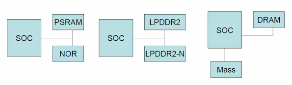
One of the most interesting slides that Floman presented at the JEDEC Mobile Forum, in my opinion, was an image that showed three processor/memory architectures for mobile phones.

The graphic looked like this:


The two architectures on the left are execute-in-place (XIP) architectures. The leftmost architecture employs pseudo-static RAM and NOR Flash as memory and executes operating-system code directly from the NOR Flash memory. The middle architecture replaces the pseudo-static RAM and NOR Flash memory with LPDDR2 SDRAM and LPDDR2-N Non-Volatile Flash memory. It’s still an execute-in-place architecture but the memory components are newer and deliver more performance with better capacity.

The architecture on the right is a shadowing architecture where the OS code is stored in a mass-storage device (NAND Flash memory) and the code is first transferred to DRAM and then executed. High-end smartphones use this architecture.


These architectural designs will hold unless a new type of memory with both fast read/write times and non-volatile storage become commercially available in the required capacities and the required cost per bit. If that happens, the smartphone will only need one memory type—perhaps that might be magnetic RAM (MRAM) or Memristor-based memory. But that’s not the situation today.

The best possible performance, said Floman, will come from Wide I/O DRAM while the UFS (Universal Flash Storage) standard appears to be poised to become the next commonly used storage medium for smartphone design. UFS “will be the next generation mass memory” for smartphones, said Floman.

All of this evolution has but a single purpose. “You will not buy your next phone from the same manufacturer unless it provides new functions,” Floman said as he concluded his keynote speech.
Posted by Ron at 4:04 AM No comments:
Labels: battery, Battery Life, Circuit, circuit expert, circuit experts, DDR, Design, Device, DRAM, expert, LPDDR, Memory, NAND, NOR, Process, PSRAM, SoC, testify

Wednesday, May 16, 2012

Intel Roadmap to 2015 and Beyond: 5nm Technology

Intel discussed roadmap to 2015 at their annual Investor meeting day on the 10th of May 2012 in Santa Clara.
Topic mentioned included the roadway to 5nm process, 450 mm wafers. See more below.

Ron


Intel Roadmap to 2015 and Beyond: 5nm Technology, Merrifield Mobile Processor, Microservers and More

http://www.cnx-software.com/2012/05/15/intel-roadmap-to-2015-and-beyond-5nm-technology-merrifield-mobile-processor-microservers-and-more/


Intel had their annual Investor meeting day on the 10th of May 2012 in Santa Clara where we would learn a few things about what's ahead for Intel and the semiconductor industry. Paul Otellini, Intel President and Chief Executive Officer, started the meeting by giving some numbers about Intel results and showing opportunities existing for cloud and data center, personal computing, mobile devices and intelligent systems (for automotive, retail and communications markets). One interesting point was the tremendous growth in data Intel expects from 2,500 Exabytes per year (7 EB/day) today to 8,000 Exabytes by 2015 which the majority of the growth lead by Big data. He also boasted about Intel technology advantage. For example, Intel introduced High-K Metal Gate technology in 2007 and competitor only got it in products last year (btw Samsung Exynos 5 uses HKMG). They recently introduced Tri-gate technology and they only expect competitors to catch up within 4 years. Finally one of the slide (see below) shows that Intel intends to be able to manufacture silicon using 10 to 5nm technology sometimes after 2015.


Intel Manufacturing Technology Road Map

The technology to achieve this feat is still at the fundamental research stage however. You can read the presentation (PDF) for more details.

Kirk Skaugen, General Manager of the PC Client Group, mainly talked about Ultrabooks which are high-performance, expensive (700 USD up) and thin notebooks. Intel Haswell Processor is designed to power Ultrabooks (in 2013) able to get 10 days of connected standby providing 20 times more efficiency than Intel iCore 5 device available in 2011. If you want to know more about the future for Intel based PC, Laptop and Ultrabook, you can read the presentation.

Diane Bryant, Vice President & General Manager of the Datacenter & Connected Systems Group, mainly talked about high end servers, but there is also a small section about microservers showing Xeon processors (Ivy Brigde) consuming 17W and the lower-end Atom Centerton SoC consuming a mere 6W. You can download the PDF presentation to know more about Intel datacenter and cloud solutions, customers and prospects.

Now let's move to smartphones and tablets with Hermann Eul & Mike Bell of Intel Mobile and Communications Group. They started by showing Intel technological know-how for mobile applications and Intel R&D commitment with over 3,000 engineer working on software for Windows, Linux (Intel is No. 2 contributor) and other operating systems, including 1,200 working on Android for mobile.

Then they gave some details about Atom Medfield processor, their first smartphone processor, which can be integrated into smartphones that support 8MPixel camera, 1080p video via HDMI and last 14 days on a single battery charge (using a 1460mA battery). They also mentioned Anandtech article showing Medfield based Lava XOLO X900 beats the competition in terms of performance (for some benchmarks) and matches the power consumption of existing smartphones.

They also showed their smartphone platform roadmap with processors for both the high end and lower end segments of the market.


Intel Smartphone Platform Roadmap

At the higher-end, we would get:
*Intel Atom Z2580 with Intel XMM 7160 LTE + 2X HSPA+ providing twice the performance of Medfield.
*Merrifield processor with XXM 7260 using 22nm manufacturing process.

and the lower-end:
*Intel Atom Z2000 @ 1GHZ with XMM 6265 (HSPA+)
*Intel Atom 6331 (22nm)

as well as future processors based on 14nm technology.
Intel also provided their tablet roadmap with Clover Trail 1.8 GHz 32nm processor (2012), Bay Trail 22nm processor (2013) and next generation processor (no name yet) using 14nm process (2014).

Have a look at the presentation for more information.

Brian Krzanich, Chief Operating Officer, gave a presentation about manufacturing and fabs which I would not normally mention in this blog, were it not for this slide:


Revenue per Company and Factory Cost Depending on Wafer Size


Currently, silicon Fabs use 200mm wafers which requires company to generate 3 to 5 billions in revenue to stay afloat representing all companies in the chart above (Elpida recently filled for bankruptcy before being bought by Micron). Now some companies starts to move to 300mm. A manufacturing site designed for this type of wafer requires 9 to 12 billions in revenues (shown in green above), but as it scales it becomes much more cost effective than a 200mm wafer Fab. That means that companies such as Freescale, NXP Broadcom and AMD would eventually have to go Fabless to survive, be bought or go bankrupt. After 2015, Fabs designed for 450mm wafer will start to show up (I'm pretty sure there is a mistake on the slide above and "300mm Fab" should read "450mm Fab"). This type of Fab requires 15 billions in revenues according to Intel, which would means that only 2 or 3 companies in the world, namely Intel, Samsung and possibly TSMC will be large enough to have manufacturing sites, unless companies such as Texas Instruments and Toshiba buy smaller players in the meantime.

If you are interested, you can check the PDF.

There were also two other presentations by the sales team and the CFO. You can listen to the webcast and access all the presentation slides on Intel Corporation 2012 Investor Meeting
Posted by Ron at 5:01 AM No comments:
Labels: 450mm, 5nm, Circuit, circuit expert, circuit experts, Design, Device, expert, Fab, industrial, industry, Manufacturing, nm, Process, testify

Tuesday, May 15, 2012

Hynix Next Gen. NAND Flash

In December 2011, at the IEDM conference Hynix presented their version of the next generation of NAND flash (smaller than 20nm). Key developments presented: "A middle-1x nm design rule multi-level NAND flash memory cell (M1X-NAND) has been successfully developed for the first time.

1) Quad spacer patterning technology (QSPT) of ArF immersion lithography is used for patterning mid-1x-nm rule wordline (WL). In order to achieve high performance and reliability, several integration technologies are adopted, such as

2) advanced WL air-gap process,

3) floating gate slimming process, and

4) optimized junction formation scheme. And also, by using

5) new N±1 WL Vpass scheme during programming, charge loss and program speed are greatly improved."
See more details below.
Ron


A middle-1X nm NAND flash memory cell (M1X-NAND) with highly manufacturable integration technologies
 Joowon Hwang, Jihyun Seo, et al., Hynix Semiconductor Inc.
5/14/2012 3:21 PM EDT
 Editor’s note: This work was first presented at the 2011 IEEE International Electron Devices Meeting (IEDM) and appears here courtesy of the IEEE.

For more information about IEDM 2012 (San Francisco, CA; December 10-12), click here. A middle-1x nm design rule multi-level NAND flash memory cell (M1X-NAND) has been successfully developed for the first time.
1) Quad spacer patterning technology (QSPT) of ArF immersion lithography is used for patterning mid-1x-nm rule wordline (WL). In order to achieve high performance and reliability, several integration technologies are adopted, such as 2) advanced WL air-gap process, 3) floating gate slimming process, and 4) optimized junction formation scheme. And also, by using 5) new N±1 WL Vpass scheme during programming, charge loss and program speed are greatly improved. As a result, mid-1x-nm design rule NAND flash memories has been successfully realized.

The NAND flash memory cell has been scaled down to the 2x [1,2,3] and 2y nm [4] generations aggressively. As scaling down of a cell size, many serious scaling problems were caused in 2x and 2y nm generation, however they were solved or managed by process, device, and system solutions. For further scaling down beyond 2y nm, we face new scaling limitations such as patterning limitation of ArF immersion spacer patterning technology (SPT), more severe control gate (CG) poly-Si filling problems between floating gates (FGs), and high electric field and charge loss problem between WLs. This paper describes several new advanced processes and operation schemes to overcome these problems, as shown in Table 1. As a result, M1XNAND flash cell is successfully implemented with highly manufacturable integration technologies.

Table 1: Major issues and solution of mid-1x cell technology. M1X-NAND cell process Figure 1 shows the layout of M1X-NAND flash cells. The half pitch of WL is middle-1x nm. The BL contacts are formed staggered arrangement and a string has several dummy WLs. In order to pattern middle-1x nm design rule WLs, QSPT is intensively developed to overcome limitation of ArF immersion SPT. Figure 1: Layout of Mid-1x-nm NAND (M1X-NAND) string with dummy WLs. The half pitch of WL is mid-1x-nm. As shown in Figure 2, first patterns are formed by photolithography and the two times combination of previous formed pattern and spacer are formed final patterns. Figure 2: Schematic diagram of QSPT (Quad Spacer Patterning Technology) key fabrication steps. Two times spacer patterning is used to make mid-1x patterning. The WL critical dimension (CD) of QSPT, which plays a very important role of Vth distribution factor, is precisely controlled less than 1.5% uniformity (see figure 3). QSPT is successfully adopted for mid-1x-nm design rule NAND cell patterning. Figure 3: Location dependence of WL CD variation of QSPT gate patterned NAND string. WL CD is precisely controlled under 1.5% uniformity. Figure 4 shows cross-sectional TEM micrographs of M1X-NAND cell, (a) along WL-direction, and (b) along BL-direction. Figure 4: Cross-section TEM view of the cell, (a) along WL direction, (b) along BL direction. The CGs are well patterned with middle-1x nm half pitch. The floating gate slimming process can achieve the void-free filling of CG poly-Si and wider active area CD, which can obtain large cell current. An electrical depletion in CG poly-Si is greatly suppressed by this void-free process. As a result, BL interference is successfully improved 20% compared with conventional process (see figure 5). The CG CoSi height was selected reasonably to achieve optimized gate shape and decrease WL RC delay for improvement program performance. Figure 5: The simulated results of BL interference with FG slimming scheme. BL interference can be improved to 20%. Cell performance To suppress charge loss (Q-loss) between CG and neighbor FG due to lateral high electric field during program, we have adopted an advanced CoSi-based WL air-gap process that has an air-gap portion above 50% between WLs. As shown in Figure 6(a), the electric field between CG and neighbor FG can be reduced 20% by an advanced CoSi-base WL air-gap. However, reduction electric field by WL airgap is not sufficient to prevent charge loss perfectly because of scale-down issues at mid-1x-nm cell size. So N±1 WL bias control scheme were adopted within WL air-gap. As a result we can also reduce the electric field 15% additionally (see figure 6(a)). Figure 6: (a) Electric field between CG and neighbor FG during programming. (b) 3-D e-field simulation with programmed PV3 neighbor cell. The electric field at point A can be reduced by air-gap and N±1 WL bias control. Then the advanced air-gap and N±1 WL scheme can greatly alleviate charge loss between CG and neighbor FG by decreasing electric field, as shown in Figure 7. Furthermore, as shown Figure 8, PGM speed is improved by N±1 WL scheme, because FG potential of program cell increase by cross coupling effect between WL and neighbor FG. Figure 9 shows the cell coupling ratio with and without air-gap. Cell coupling ratio can be also improved by air-gap due to reducing capacitance of WL direction. Figure 7: Improvement of charge loss with N±1 WL bias control method. Charge loss is greatly decreased to ~300mV by applying Vpass+2V to neighbor N±1 WL. Figure 8: Improvement of PGM speed with N±1 bias control method. Figure 9: Cell coupling ratio as technology shrinkage. Read current reduction is also major issue because of higher bulk doping for suppressing short channel effects in mid-1x-nm cell transistors. A new advanced junction scheme of cell and select transistor is adopted to maximize read current and reduce leakage current in unselected block (see figure 10). Figure 10: Read current with/without select Tr. junction optimization. Read current can be improved by select Tr. junction optimization. Cell Vth Distribution Figure 11 shows cell Vth distributions for the multi-level M1X-NAND cells. The Vth distributions have normal shapes and are well separated to three MLC states. This result confirms that M1X-NAND cell technology can be applied for high density MLC. Figure 11: Three-level programmed Vth distributions of M1X-NAND cells. Vth distributions are well separated to three MLC states. A highly manufacturable mid-1x-nm NAND flash memory (M1X-NAND) has been developed with new integration technologies, such as QSPT, advanced WL air gap process, floating gate slimming process, and optimized junction formation scheme, to overcome scaling limits of mid-1x-nm technology. The excellent device characteristics and reliability are achieved successfully. And also, a new N±1 WL Vpass scheme during programming has been also adopted to overcome WL-to-WL high field issue. Then, we have demonstrated a middle-1x nm-generation NAND flash memory (M1X-NAND) with high performance and reliability. References 1 K. Prall, et al., “25nm 64Gb MLC Technology and Scaling Challenge,” IEEE IEDM Technical Digest, pp. 102-103, 2010. 2. C. Lee, et al., “A Highly Manufacturable Integration Technology for 27nm a and 3bit/cell NAND Flash Memory,” IEEE IEDM Technical Digest, pp. 98-101, 2010. 3. H. Shim, et al., “Highly Reliable 26nm 64Gb MLC E2NAND (Embedded -ECC & Enhanced-efficiency Flash Memory with MSP (Memory Signal Processing) Controller,” VLSI Symp. Technical Digest, pp. 216-217, 2011. 4. K. Lee, et al., “A Highly Manufacturable Integration Technology of 20nm Generation 64Gb Multi-Level NAND Flash Memory,” VLSI Symp. Technical Digest, pp. 70-71, 2011. About the authors This article was contributed by the Flash Device Development & Advanced Process Team, R&D Division, Hynix Semiconductor Inc. The authors include J. Hwang, J. Seo, Y. Lee, S. Park, J. Leem, J. Kim, T. Hong, S. Jeong, K. Lee, H. Heo, H. Lee, P. Jang, K. Park, Myungshik Lee, S. Baik, J. Kim, H. Kkang*, M. Jang*, J. Lee*, G. Cho, J. Lee, B. Lee*, H. Jang, S. Park, J. Kim*, S. Lee, S. Aritome, S. Hong and S. Park
Posted by Ron at 6:42 AM No comments:
Labels: Circuit, circuit expert, circuit experts, Design, Device, expert, Flash, floating gate, industrial, manufacture, Manufacturing, memory testify, NAND, nm, Process

Wednesday, May 9, 2012

Nvidia #1 at TSMC Fab? Nvida has Priority for 28nm capacity

"TSMC has given priority to Nvidia for 28nm capacity, according to industry sources" (see below).

Nvidia has been unsatisfied with TSMC's 28nm process
Photo: Monica Chen, Digitimes file photo


Complaining publicly did not hurt - see March 26, 2012 blog Nvidia: TSMC 20nm Essentially Worthless 


Ron


TSMC gives priority to Nvidia for 28nm capacity

http://www.digitimes.com/news/a20120509PD211.html?mod=2
Monica Chen, Taipei; Joseph Tsai, DIGITIMES [Wednesday 9 May 2012]

Taiwan Semiconductor Manufacturing Company (TSMC) has given priority to Nvidia for 28nm capacity, according to industry sources.
Since Nvidia has been unsatisfied with TSMC's 28nm process, while the company has also not refuted rumors that the company may cooperate with Samsung Electronics or Globalfoundries, TSMC, to sooth Nvidia, has put the GPU maker on its supply priority, allowing Nvidia to be able to release its 28nm GPUs on schedule in May and June.
The same situation has also happened previously with Qualcomm, which had said it would consider outsourcing orders to other wafer foundries, and successfully gained TSMC's promise for supply priority.
With both Qualcomm and Nvidia achieving supply priority from TSMC, players that are also waiting for TSMC's 28nm capacity, are expected to be affected.


Posted by Ron at 7:19 AM No comments:
Labels: 20nm, 28nm, Circuit, Design, expert, GPU, Graphic, Intel, nm, Nvidia, Process, processor, scaling, Semiconductor, testify, TSMC, wafer, witness, yield

Monday, May 7, 2012

First DDR4 DRAM from Micron

Micron Announces Its First Fully Functional DDR4 DRAM Module

http://www.legitreviews.com/news/13055/

Micron today announced development of its first fully functional DDR4 DRAM module. The company has begun sampling and has received feedback from major customers to support quick implementation for applications in 2013. Codeveloped by Nanya and based on Micron's 30-nanometer (nm) technology, the 4-gigabit (Gb) DDR4 x8 part is the first piece of what is expected to be the industry's most complete portfolio of DDR4-based modules, which will include RDIMMs, LRDIMMs, 3DS, SODIMMs and UDIMMs (standard and ECC). It is expected that the enterprise and micro-server markets will take full advantage of the new features and specifications designed into DDR4, accelerating early adoption of the technology. In addition, the fast-growing ultrathin client and tablet markets will also benefit from new opportunities enabled by the power savings and performance features of Micron's DDR4. As JEDEC finalizes the DDR4 specifications, Micron is positioned to quickly become fully compliant with its 30nm 4Gb DDR4 part. Full sampling to key partners began earlier this year and volume production is planned for 4Q12. Sounds like we might be seeing some DDR4 platforms in 2013!
"With the JEDEC definition for DDR4 very near finalization, we've put significant effort into ensuring that our first DDR4 product is as JEDEC-compatible as it can be at this final stage of its development," said Brian Shirley, vice president for Micron's DRAM Solutions Group. "We've provided samples to key partners in the market place with confidence that the die we give them now is the same die we will take into mass production."

Additional information on DDR DRAM Memory
Posted by Ron at 8:43 AM 1 comment:
Labels: 3DS, Circuit, circuit expert, circuit experts, DDR, ddr4, Design, DRAM, ECC, expert, LRDIMM, manufacture, Manufacturing, Memory, moudle, RDIMMs, SODIMM, testify, testimony, UDIMM

Friday, May 4, 2012

Micron Technology Likely Winner, Buying Chipmaker Elpida Memory

"Micron likely winner in bidding for Japan's Elpida-NHK" as predicted with details by Businessweek in Feb. 27, 2012 (see below)


Ron Maltiel


Micron Biggest Winner as Elpida Bankruptcy Sidelines Rival Tech

http://www.bloomberg.com/news/2012-02-28/micron-biggest-winner-as-elpida-bankruptcy-sidelines-rival-tech.html


Micron Technology Inc. (MU) will probably emerge as the top winner from the bankruptcy ofElpida Memory Inc. (6665), whose filing yesterday sidelines the last Japanese maker of computer memory chips and gives rivals the chance to scoop up factories on the cheap.
Elpida filed for Japan’s biggest bankruptcy in two years after chip prices plunged and it failed to win a second government bailout. The elimination of a top maker of dynamic random access memory would give the rest of the industry more control over production, helping to ease the price swings that have left Micron unprofitable for six of the past 10 years.
The headquarters building of Micron Technology Inc. in Boise, Idaho. Micron shares jumped 7.7 percent yesterday amid speculation that the company, the fourth-largest DRAM maker, might seek to acquire some of Elpida’s plants. Photographer: Matthew Staver/Bloomberg
Elpida Memory Inc. memory chips are displayed in this arranged photograph in Tokyo, Japan. Photographer: Tomohiro Ohsumi/Bloomberg

Elpida’s creditors will look for ways to recoup losses through the sale of such assets as a plant in Hiroshima valued at $1 billion by Sanford C. Bernstein & Co. For potential buyers such as Micron, that price tag would be about a fifth of the cost of building a new equivalent facility. That would fit with Micron’s strategy of trying tobuy up capacity cheaply, rather than making acquisitions that outstrip the company’s $1.9 billion in cash and compel it to take on debt.

“Micron is clearly the winner,” said Dan Berenbaum, a New York-based analyst at MKM Partners LP. “Now it’s a question of how much does Micron pay for the assets.”

Micron shares jumped 7.7 percent yesterday amid speculation that the company, the fourth-largest DRAM maker, might seek to acquire some of Elpida’s plants. Dan Francisco, a spokesman for Boise, Idaho-based Micron, declined to comment.

Elpida has facilities that are responsible for about 18 percent of DRAM industry output, making it the No. 3 supplier. A push to take the plants offline or use them for other kinds of chips would help ease oversupply and stem industrywide losses.

Falling DemandThe computer-memory industry has been grappling with a decline in demand, brought on by a global consumer shift to smartphones and tablet computers, which need less memory and typically use a different type of chip.

Elpida’s troubles were exacerbated by DRAM prices falling below the cost of production. Industry sales last year dropped 26 percent to $29.2 billion, according to an estimate by Gartner Inc. That followed a 72 percent surge in 2010.

The Japanese chipmaker was the product of a 1999 merger between the memory businesses of NEC Corp. and Hitachi Ltd., which exited the industry.
‘Ten-Foot Pole’If Micron makes a bid for some DRAM facilities, Elpida’s creditors will get an offer that’s “tough to swallow,” because the U.S. company knows it’s not likely to face any competition, said Hans Mosesmann, an analyst at Raymond James & Associates Inc.

“Nobody else is going to touch DRAM with a ten-foot pole,” said Mosesmann, who has a “strong buy” rating on Micron shares. “Micron is very practical. They don’t want all of Elpida.”
Earlier this month, Micron’s management told Mosesmann and other analysts the company is monitoring events in Japan to see if there are opportunities. Executives declined to comment on whether Elpida is one of them and what the company might do.
“It just doesn’t feel like there’s going to be any fresh capital put into the DRAM business,” Micron President Mark Adams said in an interview on Feb. 9. “If we’re right, then the industry is mature enough that consolidation could make a lot of sense.”
Elpida has total debt of about $4 billion and has reported five straight quarters of losses. Micron, which has been making acquisitions and driving industry consolidation for more than 10 years, has about $1.95 billion of debt, approximately equal to its cash reserves. The company has a target range for its debt- to-capital ratio of 20 percent to 25 percent. Its current cash plus market capital of $8.4 billion give it a debt-to-capital ratio of about 18 percent, according to data compiled by Bloomberg.
Debt GuidelinesIf Micron stays within those guidelines -- giving it the latitude to borrow about another $500 million -- it’s not going to have enough leeway to buy its Japanese rival, said Daniel Amir, a San Francisco-based analyst at Lazard Capital Markets LLC.
“They probably won’t just buy out Elpida,” Amir said. “They are not willing to break the bank. It’s not like they’re going to spend $2 billion.”

Samsung Electronics Co., which dominates the memory-chip business and is the only consistently profitable company in the industry, has said it will concentrate on running its own business, making it an unlikely bidder for Elpida’s assets.
“Samsung is not going to come to their rescue,” said Raymond James’s Mosesmann.
Profit StruggleExcluding Samsung -- which is also the world’s second- largest maker of mobile phones and the biggest maker of liquid crystal displays -- DRAM makers have struggled to make money.
Matching supply with demand poses a constant challenge in the market for DRAM for personal computers, where plants take years to come online and can’t be shut down cheaply. With factories costing billions of dollars to build, companies such as Elpida have found themselves facing debts they have trouble repaying.
In six of the past 10 years, industry companies have spent more cash than their operations have generated. Even including Samsung, whose share price has more than tripled, memory makers as a group have lost 40 percent of their market value since October 2002.
If output from Elpida’s plants is slowed down or halted, all of its rivals will benefit as supply gets closer to demand and prices stabilize, according to Shawn Webster, an analyst at Macquarie Capital USA Inc.
“Any time a competitor is in distress, it’s a positive for everybody else,” said Webster. “If you pull supply offline, that could help everybody in the DRAM industry.

Micron CEOEarlier this month, Micron lost longtime Chief Executive Officer Steve Appleton, who died in a plane crash. Mosesmann and other analysts speculated that his death might slow any possible negotiations for industry consolidation, because Appleton had been the driving force behind previous transactions.

Micron, which got its start with an investment from local potato magnate J.R. Simplot, became one of the largest makers of computer memory when it bought the memory operations of Texas Instruments Inc. in 1998. Since then, it has acquired plants from Toshiba Corp., bought control of a Japanese joint venture, and formed partnerships with Taiwan’s Nanya Technology Corp. and Intel Corp. to secure access to more production.
In 2008, as Germany’s Qimonda AG headed for bankruptcy and sought investments, Micron bought out its interest in Inotera Memories Inc. (3474)Qimonda subsequently went out of business, and its chipmaking equipment was sold off.
Micron has also walked away from opportunities. In April 2002, it abandoned a transaction under which it would have acquired the memory operations of South Korea’s Hynix Semiconductor Inc., the second-largest DRAM maker, after the companies couldn’t agree on terms.
‘In No Rush’One way that Micron might consider a purchase of Elpida would be if it could get cheap financing for a transaction from Elpida’s creditors, which are facing the dilemma of knowing that restructuring the company’s debt wouldn’t be enough to make it competitive again, according to Betsy Van Hees, a San Francisco- based analyst at Wedbush Securities. Elpida needs more money to invest in making its production more efficient, she said.
When asked on Feb. 10 whether he would take Micron’s debt level above 25 percent of its capital to make an acquisition that would consolidate the industry, Chief Executive Officer Mark Durcan told analysts he was going to be “very careful about putting the company in a position where we’re not confident we can deal with any additional debt.”
Still, he would consider taking the debt ratio higher if there was a good enough opportunity, he said.

Posted by Ron at 6:24 AM No comments:
Labels: chip, Circuit, Design, Device, elpidia, expert, Fab, Fabrication, Manufacturing, Micron, nm, Process, testify, witness
Older Posts Home
Subscribe to: Posts (Atom)

Blog Archive

  • ▼  2017 (2)
    • ▼  Nov 2017 (2)
      • Expert Testimony with Ron Maltiel
      • 5th Update: Mergers/ Potential Mergers 2015-7 (lat...
  • ►  2016 (20)
    • ►  Nov 2016 (1)
    • ►  Sep 2016 (1)
    • ►  Jul 2016 (2)
    • ►  Jun 2016 (4)
    • ►  May 2016 (1)
    • ►  Apr 2016 (1)
    • ►  Mar 2016 (3)
    • ►  Feb 2016 (1)
    • ►  Jan 2016 (6)
  • ►  2015 (24)
    • ►  Dec 2015 (4)
    • ►  Sep 2015 (2)
    • ►  May 2015 (6)
    • ►  Apr 2015 (3)
    • ►  Mar 2015 (1)
    • ►  Feb 2015 (2)
    • ►  Jan 2015 (6)
  • ►  2014 (36)
    • ►  Dec 2014 (4)
    • ►  Nov 2014 (4)
    • ►  Oct 2014 (2)
    • ►  Sep 2014 (3)
    • ►  Aug 2014 (3)
    • ►  Jul 2014 (3)
    • ►  Jun 2014 (2)
    • ►  May 2014 (1)
    • ►  Apr 2014 (5)
    • ►  Mar 2014 (4)
    • ►  Feb 2014 (2)
    • ►  Jan 2014 (3)
  • ►  2013 (60)
    • ►  Dec 2013 (1)
    • ►  Nov 2013 (6)
    • ►  Oct 2013 (4)
    • ►  Sep 2013 (4)
    • ►  Aug 2013 (3)
    • ►  Jul 2013 (9)
    • ►  Jun 2013 (2)
    • ►  May 2013 (6)
    • ►  Apr 2013 (3)
    • ►  Mar 2013 (5)
    • ►  Feb 2013 (7)
    • ►  Jan 2013 (10)
  • ►  2012 (105)
    • ►  Dec 2012 (2)
    • ►  Nov 2012 (7)
    • ►  Oct 2012 (12)
    • ►  Sep 2012 (9)
    • ►  Aug 2012 (12)
    • ►  Jul 2012 (14)
    • ►  Jun 2012 (11)
    • ►  May 2012 (15)
    • ►  Apr 2012 (9)
    • ►  Mar 2012 (14)
  • ►  2011 (1)
    • ►  Mar 2011 (1)
  • ►  2010 (1)
    • ►  Jan 2010 (1)
  • ►  2009 (6)
    • ►  Jun 2009 (5)
    • ►  May 2009 (1)

GlobeNewswire News

RSS Feed Widget

Semiconductor Industry Developments

  • Semiconductor Expert
  • News
  • Patents, ITC & Federal Infringements
  • Electronic Circuit News, Tutorials
  • Process News, Tutorials
  • FLASH Educational Links
  • FLASH News
  • Resources
  • Search the Site
  • Twitter address

Twitter Live Stream

About Me

Unknown
View my complete profile

TraceMyIP.org

Simple theme. Powered by Blogger.