Showing posts with label circuit expert. Show all posts

Wednesday, September 24, 2014

Apple's iPhone 6 A8 Teardown

Chipworks has been quick to teardown Apple's A8 processor, which is the secret sauce driving the new iPhone 6. Some details of the teardown are discussed below.

"Apple has spent quite a bit of die size on improving performance through more complex CPU and GPU architectures and miscellaneous feature additions."


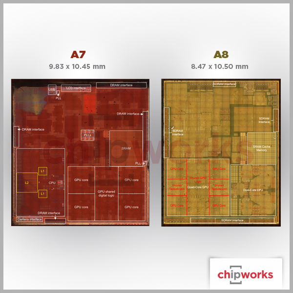
A8 is fabricated on TSMC 20nm process while  A7 was manufactured on Samsung 28nm process. Shrinking the transistors gate to 20nm enables the CPU to operate faster. While limiting A8 to 4 GPU cores and not 6 help to reduce the new iPhone power.


Ron
Insightful, timely, and accurate semiconductor consulting.
Semiconductor information and news at - http://www.maltiel-consultin


Chipworks Disassembles Apple's A8 SoC: GX6450, 4MB L3 Cache & More

by Ryan Smith on September 23, 2014 1:00 PM EST

One of the more enjoyable rituals with Apple’s annual iPhone launch is the decapping, deconstruction, and photographing of the processor die at the heart of Apple’s newest SoC.  While we can learn a lot about the SoC from software, for some things there’s just no replacement for looking at the hardware itself and counting the functional blocks present. And this year, as in past years, the honor of being the first to tear apart the SoC goes to Chipworks.
For determining the layout of A8, Chipworks reached out to us to solicit our input on their die shot, and after some rounds of going back and forth we believe we’ve come to a solid determination of some of A8’s features and how it has been configured. So let's dive in.
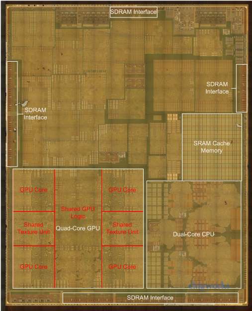
First and foremost we’ll start with A8’s GPU, as this was one of the hardest elements to analyze in software. Based on Apple’s 50% performance improvement we had previously speculated that A8 contained an Imagination PowerVR GX6650. However as we noted back then, a die shot would reveal all, and right on schedule it has.
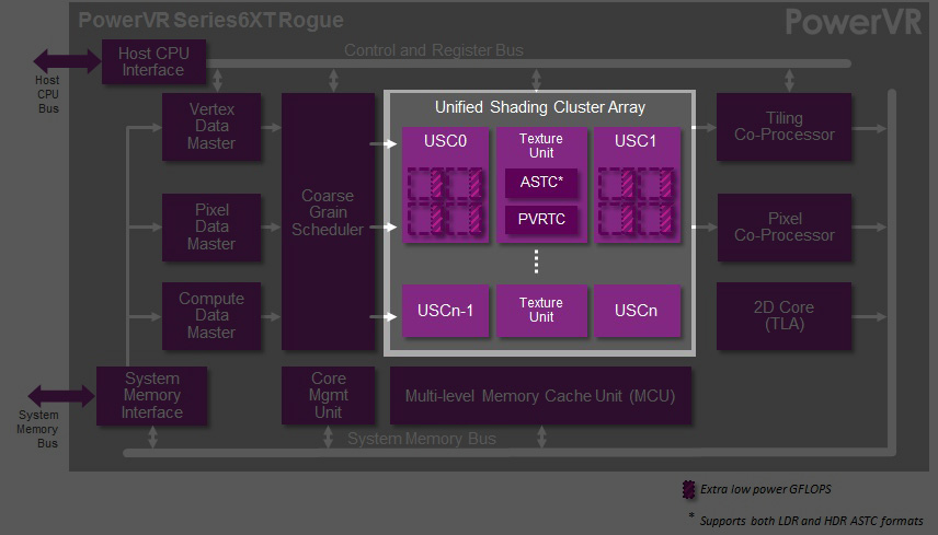
A close analysis of the die shot makes it clear that there are only 4 GPU cores available and not 6, which immediately rules out the 6 core GX6650 we were previously expecting. Instead with 4 cores present this is conclusive proof that Apple is using the smaller 4 core GX6450 on A8, the direct successor to the G6430 used on the A7. GX6450 induces some performance optimizations along with some feature updates – including ASTC support, which Apple’s documentation has already confirmed is present – so its inclusion here is a natural progression for Apple.
On A8 and its 20nm process this measures at 19.1mm2, versus A7’s 22.1mm2 G6430. As a result Apple is saving some die space compared to A7, but this is being partially offset by the greater complexity of GX6450 and possibly additional SRAM for larger caches on the GPU. Meanwhile looking at the symmetry of the block, it’s interesting that the blocks of texturing resources that every pair of GPU cores share is so visible and so large. With these resources being so big relative to the GPU cores themselves, you can see why Imagination would want to share them as opposed to building them 1:1 with the GPU cores.
Meanwhile opposite the GPU we have the CPU block. Unlike the GPU the CPU block has seen some significant shrinking, which Chipworks estimates is down from 17.1mm2 in A7 to 12.2mm2 in A8. In A7 Cyclone did not lend itself to easily picking apart the individual CPU cores, and neither does the CPU here in A8. We’ll be looking at the new CPU’s architecture in-depth in our iPhone 6 review, but for now it’s safe to say that while this is definitely derived from Cyclone, Apple has added a few tweaks over the last year that make it an even more potent CPU than the first Cyclone. Meanwhile based on this die shot Chipworks believes that the L2 cache has been reorganized to a per-core design, as there is no obvious single block of L2 on A8 like there was A7.
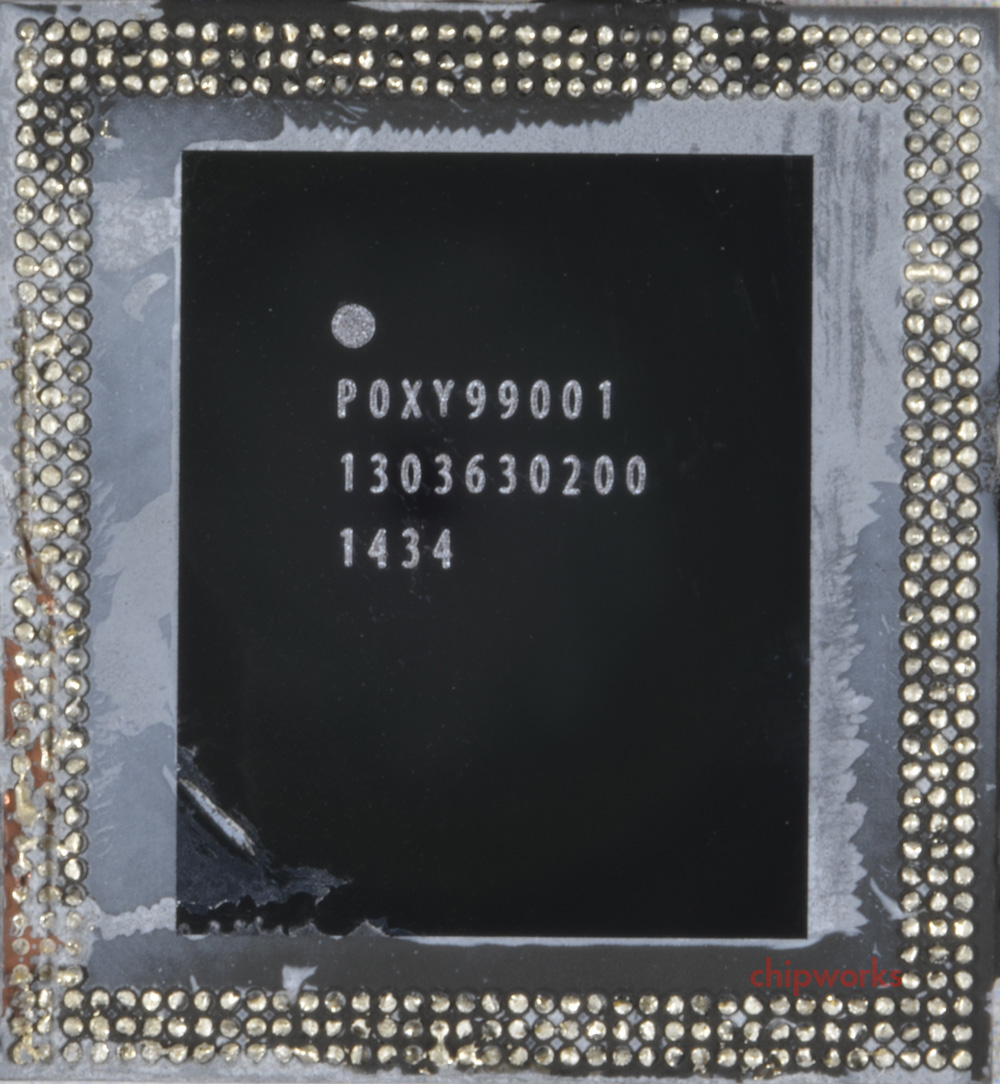
A8 With PoP DRAM Removed
The final major identifiable block on A8 is once again the SRAM cache memory. On A7 we discovered that this block was 4MB and was responsible for servicing the GPU and CPU. On A8 this block is similarly present and serving the same role. This 4MB of SRAM ends up being quite big despite the shrink from 28nm to 20nm, and while at first glance it seems like it should be larger than 4MB given the relative size, in practice what has happened is that the individual SRAM cells have not shrunk by a full 50%. Chipworks estimates the cell size to now be about 0.08µm2, versus 0.12µm2 on A7, which is closer to a 33% shrink that a 50% shrink. As a result the SRAM cache still takes up a fair bit of space, but the value of being able to serve larger memory requests without having to go off-die continues to be immense.
Apple A8 vs A7 SoCs
 Apple A8 (2014)Apple A7 (2013)
Manufacturing ProcessTSMC 20nm HKMGSamsung 28nm HKMG
Die Size89mm2104mm2
Transistor Count~2B"Over 1B"
CPU2 x Apple Enhanced Cyclone ARMv8 64-bit cores2 x Apple Cyclone ARMv8 64-bit cores
GPUIMG PowerVR GX6450IMG PowerVR G6430
Overall, Chipworks’ analysis points to A8 being fabbed on TSMC’s 20nm process. This makes A8 among the first SoCs to receive the 20nm treatment. Thanks to this smaller node Apple has been able to build in additional features to the SoC while simultaneously shaving off around 15% of their die size. Chipworks estimates the final die size of A8 to stand at 89mm2, versus the 104mm2 for the Samsung 28nm based A7. Chipworks notes that if this were a straight shrink that one would expect the A8 to be closer to 50% the size of A7 (though not all logic can shrink quite that well), which indicates that Apple has spent quite a bit of die size on improving performance through more complex CPU and GPU architectures and miscellaneous feature additions.
Wrapping things up, we’ll be back later this month with our review of the iPhone 6 family and our full analysis of the A8 SoC. So until then stay tuned.
Thursday, September 18, 2014

SanDisk ULLtraDIMM gaining traction

Huawei servers add flash DIMMs to their RH8100 servers (see below).

Are Dell, HP and Cisco next?


More about SanDisk ULLtraDIMMs


Ron
Insightful, timely, and accurate semiconductor consulting.
Semiconductor information and news at - http://www.maltiel-consulting.com/


Huawei: Our servers are a flash in the DRAM – thanks, SanDisk

Chinese box builder flings ULLtraDIMMs into processor memory bus – IBM, Dell next?

Monday, July 21, 2014

Bottlenecks: DRAM & Moore's Law

In addition to Moore's law slowing there are bottlenecks between the memory device and the CPU. 


The article below discusses
" How long will it will it take to find a technology so fundamentally different and better from anything we have today that we can do away with the DRAM latency and power consumption bottleneck?

There is a need for -
"A new RAM technology that cut main memory accesses by an order of magnitude would be reason enough to reevaluate the entire balance of resources on a microprocessor. If accessing main memory was as fast as accessing the CPUs cache, you might not need cache on the CPU die or package at all — or at least, you wouldn't need anything beyond L1 and maybe a small L2."

More about Moore's Law bottleneck from March 2012 Moore's Law End? (Next semiconductors gen. cost $10 billion)

Ron
Insightful, timely, and accurate semiconductor consulting.
Semiconductor information and news at - 
http://www.maltiel-consulting.com/


DRAM is pretty amazing stuff. The basic structure of the RAM we still use today was invented more than forty years ago and, just like its CPU cousin, it has continually benefited from the huge improvements that have been made in fabrication technology and density improvements. Less than ten years ago, 2GB of RAM was considered plenty for a typical desktop system — today, a high-end smartphone offers the same amount of memory but at a fifth of the power consumption.
After decades of scaling, however, modern DRAM is starting to hit a brick wall. Much in the same way that the CPU gigahertz race ran out of steam, the high latency and power consumption of DRAM is one of the most significant bottlenecks in modern computing. As supercomputers move towards exascale, there are serious doubts about whether DRAM is actually up to the task, or whether a whole new memory technology is required. Clearly there are some profound challenges ahead — and there’s disagreement about how to meet them.

What’s really wrong with DRAM?

A few days ago, Vice ran an article that actually does a pretty good job of talking about potential advances in the memory market, but includes a graph I think is fundamentally misleading. That’s not to sling mud at Vice — do a quick Google search, and you’ll find this picture has plenty of company:
DRAM scaling
The point of this image is ostensibly to demonstrate how DRAM performance has grown at a much slower rate than CPU performance, thereby creating an unbridgeable gap between the two system. The problem is, this graph no longer properly illustrates CPU performance or the relationship between it and memory.  Moore’s law has stopped functioning at anything like its historic level for CPUs or DRAM, and “memory performance” is simply too vague to accurately describe the problem.
The first thing to understand is that modern systems have vastly improved the bandwidth-per-core ratio compared to where we sat 14 years ago. In 2000, a fast P3 or Athlon system had a 64-bit memory bus connected to an off-die memory controller clocked at 133MHz. Peak bandwidth was 1.06GB/s while CPU clocks were hitting 1GHz. Today, a modern processor from AMD or Intel is clocked between 3-4GHz, while modern RAM is running at 1066MHz (2133MHz effective for DDR3) — or around 10GB/sec peak. Meanwhile we’ve long since started adding multiple memory channels, brought the memory controller on die, and clocked it at full CPU speed as well.
ddr_memory_data_rate
The problem isn’t memory bandwidth — it’s memory latency and memory power consumption. As we’ve previously discussed, DDR4 actually moves the dial backwards as far as the former is concerned, while improving the latter only modestly. It now looks as though the first generation of DDR4 will have some profoundly terrible latency characteristics; Micron is selling DDR4-2133 timed at 15-15-15-50. For comparison, DDR3-2133 can be bought at 11-11-11-27 — and that’s not even highest-end premium RAM. This latency hit means DDR4 won’t actually match DDR3′s performance for quite some time, as shown here:

This is where the original graph does have a point — latency has only improved modestly over the years, and we’ll be using DDR4-3200 before we get back to DDR3-1600 latencies. That’s an obvious issue — but it’s actually not the problem that’s holding exascale back. The problem for exascale is that DRAM power consumption is currently much too high for an exascale system.
The current goal is to build an exascale supercomputer within a 20MW power envelope,sometime between 2018 and 2020. Exascale describes a system that has exaflops of processing power, and perhaps hundreds of petabytes of RAM (current systems max out at around 30 petaflops and only a couple of petabytes of RAM. If today’s best DDR3 were used for the first exascale systems, the DRAM alone would consume 54MW of power. Clearly massive improvements are needed. So how do we find them?

Reinvent the wheel — or iterate like crazy

There are two ways to attack this problem, and they both have their proponents. One method is to keep building on the existing approaches that have given us DDR4 and the Hybrid Memory Cube. It’s reasonably likely that we can squeeze a great deal of additional improvement out of the basic DRAM structure by stacking dies, further optimizing trace layouts, using through-silicon vias (TSVs), and adapting 3D designs. According to a recent research paper, this could cut the RAM power consumption of a 100-petabyte supercomputer from 52MW (assuming standard DDR3-1333) to well below 10MW depending on the precise details of the technology.
While 100PB  is just one tenth of the way to exascale, reducing the RAM’s power consumption by an order of magnitude is unquestionably on the right track.
DRAM-Types
The other, more profound challenge, is the idea of finding a complete DRAM replacement. You may have noticed that while we cover new approaches and alternatives to conventional storage technologies, virtually all the proposed methods address the shortcomings of NAND storage — not DRAM. There’s a good reason for that — DRAM has survived more than 40 years precisely because it’s been very, very hard to beat.
The argument for reinventing the wheel is anchored in concepts like memristorsMRAM,FeRAM, and a host of other potential next-generation technologies. Some of them have the potential to replace DRAM altogether, while others, like phase change memory, would be used as a further buffer between DRAM and NAND. The big-picture fact that Vice does get right is that discovering a new memory technology that was faster and lower power than DRAM really would change the fundamental nature of computing — over time.
It’s easy to forget that the trends we’re talking about today have literally been true for decades. 11 years ago, computer scientist David Patterson presented a paper entitledLatency Lags Bandwidth, in which he measured the improvements in bandwidth against data accesses across CPUs, DRAM, LAN, and hard drives (SSDs weren’t a thing at that time). What he found is summarized below:
Latency lags bandwidth
In every case — and in a remarkably consistent fashion — latency improved by 20-30% in the same time that it took bandwidth to double. This problem is one we’ve been dealing with for decades — it’s been addressed via branch prediction, instruction sets, and ever-expanding caches. It’s been observed that we add one layer of cache roughly every 10 years, and we’re on track to keep that with Intel’s 128MB EDRAM cache on certain Haswell processors.
A new main memory with even half standard DRAM latency would give programmers an opportunity to revisit decades of assumptions about how microprocessors should be built. A new RAM technology that cut main memory accesses by an order of magnitude would be reason enough to reevaluate the entire balance of resources on a microprocessor. If accessing main memory was as fast as accessing the CPUs cache, you might not needcache on the CPU die or package at all — or at least, you wouldn’t need anything beyond L1 and maybe a small L2.
How long will it will it take to find a technology so fundamentally different and better from anything we have today that we can do away with the DRAM latency and power consumption bottleneck? Given how such a fundamental breakthrough would be vital to our ability to reach exascale computing and beyond, though, I hope it’s soon.

Wednesday, July 9, 2014

Will NAND DIMMs take of?

Product like ULLtraDIMM (see article below) can take off  and become a major NAND SSD product line as SanDisk proves it in the market and Diablo Technologies license it to additional SSD suppliers.

More about ULLtraDIMM - Sandisk's future is far from ULLtraDIMM: Diablo tie-up holds promise Goldmine in the making for flash-DIMM server shop


This product is advancing memory system designs similar to the discussion in May 2012 blog - Apple NAND Storage in Upcoming MacBook Pros


Ron
Insightful, timely, and accurate semiconductor consulting.
Semiconductor information and news at - http://www.maltiel-consulting.com/


Will SanDisk Corp's New Product Revolutionize the Storage Industry?

In January, storage provider SanDisk  (NASDAQ: SNDK  ) announced ULLtraDIMM, a new form of flash storage that promises drastic speed increases for high-performance applications. SanDisk already has one big customer, IBM (NYSE: IBM  ) , for its ULLtraDIMMs, giving some early validation to this new technology. Let's take a closer look at ULLtraDIMMs and the effect they might have on the industry.

A bit of background
Storage, such as flash SSDs or hard disk drives, typically sits far away from the CPU and main memory. This means that there is latency due to the time it takes data to travel between the storage device and the CPU. For hard drives, this is not particularly relevant because their own internal latency is much greater than the transport latency. However, for flash, which is completely electronic and therefore much faster than hard disks, this becomes an issue.

The first approach to reducing this latency was to move flash from the drive and onto the PCIe communications bus, a step closer to the CPU. This provided an improvement, but it is not the optimal solution. PCIe still has latency compared to the memory bus, which sits right next to the CPU.

The new technology
Enter SanDisk's ULLtraDIMM, a flash storage that connects directly to the memory bus through the DIMM form factor, just like DRAM memory. Connecting to the memory bus gives ULLtraDIMMs a write latency of under 5 microseconds, compared to around 50 microseconds for PCIe SSDs. The shorter communication distance also means less power consumption, a crucial concern in densely packed enterprise servers.

Sandisk currently provides 200 GB and 400 GB ULLtraDIMMs, and users can add as many ULLtraDIMMs as they have memory slots. ULLtraDIMMs are implemented in a way that makes them look like a normal storage device to the operating system, but achieving this requires modifications to the BIOS which mean that ULLtraDIMMs are not yet plug-and-play devices.

Current and future applications
IBM has already signed up as a customer for Sandisk's ULLtraDIMMs. The enterprise giant has added some functionality to ULLtraDIMMs and rebranded them as eXFlash memory-channel storage. The new technology is available in IBM's X6 family of servers.

According to SanDisk and IBM, memory-channel storage will be useful for applications such as big data analytics, transactional databases, high-frequency trading, and virtualized environments. So far, it seems that IBM's X6 servers have been particularly popular with Wall Street firms. Speaking with EnterpriseTech, SanDisk senior director of marketing Brian Cox said, "we have all kinds of hedge funds begging us to deliver this."

What this means for the industry
It will take several more computer manufacturers to sign on in order to fully validate ULLtraDIMMs as a technology and to reveal the applications where it might best be used. SanDisk's management said that this will require evangelization and a surrounding ecosystem, and that they are continuing to invest in order to bring ULLtraDIMMs to wider adoption.  
Revenue from ULLtraDIMMs is estimated to be small in 2014. However, if ULLtraDIMMs catch on, competitors such as Micron  (NASDAQ: MU  ) (which is increasingly focusing on providing SSDs rather than selling chips as a commodity) will certainly follow with their own versions of memory bus flash. Currently, no other major flash provider is talking about this kind of technology; this means that SanDisk will have first-mover advantage for at least a few quarters.

It's also not clear yet to what extent memory-channel storage might displace PCIe or server-side flash. If the total cost of ownership for an ULLtraDIMM is comparable to or lower than current SSDs, the technology might eventually become the dominant form of flash storage. However, it is also possible that ULLtraDIMMs will complement rather than replace other forms of storage, much like flash itself did with hard disk drives in the enterprise space.

In conclusion
SanDisk has introduced a new form of flash storage called ULLtraDIMM, which sits right next to the CPU on the memory bus and provides much smaller latencies than existing solutions. In a partnership with IBM, ULLtraDIMMs have been shipping to enterprise customers, with expected applications such as high-frequency trading. While the technology certainly sounds promising and might be valuable for both SanDisk and IBM down the line, it's still too early to tell what effect this will have on the storage industry and enterprise computing in general. 
Warren Buffett: This new technology is a "real threat"At the recent Berkshire Hathaway annual meeting, Warren Buffett admitted this emerging technology is threatening his biggest cash-cow. While Buffett shakes in his billionaire-boots, only a few investors are embracing this new market which experts say will be worth over $2 trillion. Find out how you can cash in on this technology before the crowd catches on, by jumping onto one company that could get you the biggest piece of the action. Click here to access a FREE investor alert on the company we're calling the "brains behind" the technology.

Wednesday, June 18, 2014

eMMC/ eMCP - Samsung lose, Hynix gain $1.7Bil

The market of embedded flash controller grew from $6 to 9.5 Billion between 2012 to 2013 (see the article below). 

The article does not elaborate on the large increase of market share by Hynix and Toshiba. Hynix gain market share from 6.3% to 22.5% while Toshiba from 18.7% to 22.5%.

2013 Rank
Company
2012 Share
2013 Share
1
Samsung
56.6%
35.6%
2
Toshiba
18.7%
22.5%
3
SK Hynix
6.3%
22.5%
4
SanDisk
15.5%
14.0%

Wondering what is the cause for Hynix $1.68 Billion growth? It will be interesting to compare to the market share of the overall Flash NAND memory market shares. Is Apple behind Hynix growth?

Interesting to see today news that Quarterly Profits of Samsung Electronics Forecast to Drop
IT & Mobile Division, which accounted for over 60 percent of the electronics giant’s sales and business profits last year. The division’s smartphone and tablet PC shipments are estimated to have declined significantly in the current quarter. “According to our forecast, smartphone and tablet PC shipments have fallen at least 10 percent and approximately 20 percent from the preceding quarter, respectively,” said research analyst Song Myung-sup at HI Investment & Securities”


Ron
Insightful, timely, and accurate semiconductor consulting.
Semiconductor information and news at - http://www.maltiel-consulting.com/


Janine Love
6/16/2014 05:15 PM EDT 

Recently, Gartner released a report, "Market Share Analysis: eMMC and eMCP Vendors by Revenue, Worldwide, 2013." The top ranked vendor for eMMC and eMCP market was Samsung Electronics, with 35.6% of worldwide revenue (around $3.317 billion). The top four vendors, Samsung, Toshiba, SK Hynix, and SanDisk, claimed 95.4% revenue share in 2013, up from 90% the previous year. Sales of eMCPs saw higher growth in 2013 than eMMCs. In the report, Gartner attributes this to the increased support of eMCPs by application vendors for low-cost smartphones.


Table: Vendor revenue for eMMCs and eMCPs, worldwide, 2012-2013 (millions of dollars).

Officially known as JESD84-B50: Embedded MultiMediaCard (e.MMC), Electrical Standard (5.0), eMMC memory is a JEDEC standard that is currently in version 5.0. As JEDEC defines it, eMMC is an embedded non-volatile memory system that includes flash memory as well as a flash memory controller. The aim of the standard is to simplify the application interface design and free up the host processor from some of the low-level flash memory management tasks. About two years ago, we saw the introduction of embedded multi-chip package (eMCP) memory, which is eMMC memory with an additional DRAM module, developed for low-cost smartphones in an effort to speed time to market.

Figure: Position of different mobile memory systems in relation to cost and speed.
(Source: Gartner)

Gartner's principal analyst, Brady Wang, compiled the report. He found it surprising that sales of eMCPs saw higher growth in 2013. He also noted that TLC (also known as 3-bits-per-cell) NAND solutions for both eMMC and eMCP will see high adoption in 2014, both in smartphones and tablets. This will address the market demands for high levels of storage space while lowering costs.
eMMC and eMCP memory includes controllers. Some vendors are using their in-house controllers to gain a competitive advantage. 

Wang says: Some NAND flash vendors, including SNKD, Toshiba and Samsung, still use in-house controllers. Since the geometry of NAND flash moves fast and also the configurations of NAND flash chips between vendors are slightly different, it's important to have a close relationship between controller vendors and chip vendors. That's one advantage of in-house controllers. The other advantage is the cost.

Despite the success stories, challenges remain for mobile memory, and Wang identifies speed and performance as the top ones, as mobile memory is challenged to meet the demands of high-performance processors. As a result, he expects universal flash storage (UFS) memory to see its initial adoption in the second half of 2014, but only in very high-end, flagship products to start.
The advantages of UFS memory (as compared to eMMC/eMCP memory) are better performance, higher capacity, better bandwidth, better IOPS, and optimized performance for multithreaded applications, according to Wang. UFS uses a serial interface (eMMC is a parallel interface) and asynchronous I/O (eMMC is synchronous I/O), enabling it to efficiently move data between the host processor and mass storage.

Wang notes that currently the cost and power consumption of UFS is higher than eMMC, so this will constrain its adoption. However, with the introduction of multi-core architectures that require high-performance memory, UFS is well positioned. “Although the power consumption of UFS is higher than eMMC, its energy efficiency is better,” says Wang. He expects to see UFS in high-end smartphones, tablets, and ultrabooks. eMMC will still be the best choice for mid-to-low cost mobile applications. Wang also points to SATA SSDs as competition for UFS in ultrabook applications. Finally, he notes that UFS is not backward compatible with eMMC, which will slow its adoption in applications where eMMC is already used.