Showing posts with label Device. Show all posts

Wednesday, November 12, 2014

Samsung 3D Process Pioneers Next Gen Semiconductor Devices

Samsung is leading the semiconductor industry with a two year leads in development of 3D NAND (see the article below).


The basic 3D process could be applied to other technologies beside flash such as DRAM memory or logic. It enable increasing the number of the transistors on each dies without the need to shrink the design rules below 20nm.

It is a key advantages since you do not need to develop the very difficult EUV photolitography.

More about 3D NAND in August 2013 blog - Samsung’s 1Tb SSD: 3D Vertical NAND

It make sense for Samsung to apply 3D Flash first to enterprise SSD, where the growth rate is +40%.

See also Applied Materials development work on advance patterning  - Applied Materials Develops Advanced Patterning Solution for Memory Devices


Ron
Insightful, timely, and accurate semiconductor consulting.
Semiconductor information and news at - http://www.maltiel-consulting.com/


samsung_hwaseong_2optimized.jpg

An aerial view of Samsung's Hwaseong plant.
10 NOVEMBER 2014
Samsung Electronics is working to strengthen its position in the SSD market by increasing the profitability of its semiconductor memory business.
According to industry sources on Nov. 9, Samsung established a strategy to choose 3-bit V-NAND-based SSD as a new growth engine of its semiconductor memory business.
Since the productivity of 3-bit V-NAND is twice as high as 10 nm class planar NAND flash, the V-NAND is superior in price competitiveness, data processing speed, durability, and power efficiency. Thus, if the 3-bit V-NAND is featured in SSDs, it will increase the performance and price competitiveness of SSDs.
After its success in having a system to mass produce 3-bit V-NAND at the company's semiconductor plant in Hwaseong City near Seoul early last month, the Korean chip maker started to prepare for mass production at its 3D V-NAND production facility in Xian, China.
Considering that it normally takes six months to expand a mass production system to other plants, the industry anticipates that 3-bit V-NAND will be mass produced starting in May or April of next year.
The semiconductor plant in Hwaseong City produces mainly planar NAND flash for mobile devices, and thus it manufactures less than 100,000 V-NAND 300 mm wafers per month.
In contrast, the 3D V-NAND production facility in Xian, which commenced full operations in May, manufactures 300,000 to 400,000 sheets each month. However, the facility is considered to have capacity to produce more than 700,000 sheets.
Samsung aims to strengthen its dominant position in the market by increasing its share in the SSD market through the use of 3-bit V-NAND in SSDs.
The Korean company revealed that it will feature 3-bit V-NAND in SSDs starting next year at a conference call, following its announcement of results for the third quarter at the end of October.
Samsung's decision can be interpreted to mean that it intends to widen the gap with its rival companies in the global market by featuring 3-bit V-NAND in SSDs used in a data center environment and SSDs for PCs.
Market research firm IHS Technology recently reported that the world's largest memory chip maker will record US$3.277 billion in sales from SSDs in 2014, a 60 percent year-on-year gain. Its market share is expected to increase from 26 percent to 29 percent this year, which will put the firm in the top spot, followed by Sandisk with a 19 percent share, Intel (18 percent), Toshiba (9 percent), and Micron Technology (8 percent).
Currently, Samsung is the only company in the world that produces 3D V-NAND flash memory chips. The gap with rival companies in technology is generally acknowledged to be more than two years.
- See more at: http://www.businesskorea.co.kr/article/7217/focusing-ssds-samsung-mass-produce-3-bit-3d-nand-flash-ssd#sthash.vOPJFbm8.dpuf

Wednesday, May 14, 2014

3D NAND Race is On

[Image Source: Nikkei Electronics
Since Samsung announced their development of 3D NAND on August 2013 Samsung 3D Stacked NAND Flash has Engineering Samples . The other flash manufacturers have been trying to catch up while transitioning from planar NAND to 3D NAND. See below SunDisk and Toshiba announcement of their transitions plans (more information at 3D NAND Transition: 15nm Process Technology Takes Shape ).

Some background about 3D NAND and at 3D NAND flash is coming .  Also there is an interesting discussion regarding 3D flash from 2009 between Samsung and Toshiba 3D Cells Make Terabit NAND Flash Possible .


Ron
Insightful, timely, and accurate semiconductor consulting.
Semiconductor information and news at - http://www.maltiel-consulting.com/


 NAND Flash War

Toshiba, Sandisk Partnership to Mount Serious Challenge to Samsung

14 MAY 2014
Many computer memory chipmakers worldwide are said to be working to enlarge plants that produce NAND flash memory chips.  
According to the San Kei Shimbun on May 12, Toshiba, the world’s second-largest NAND flash memory chipmaker, decided to make an investment in a 3D V-NAND flash memory production facility in partnership with US-based semiconductor company SanDisk. Both companies are going to equally share the cost of the investment and inject 700 billion yen (7.419 trillion won, US$6.843 billion) for three years at the Yokkaichi Operation plant, the company’s memory production facility in Mie prefecture, Japan. At first, they estimated the amount at 400 billion yen. However, it nearly doubled after the two firms agreed to invest in the construction of a new facility and the replacement of the existing one.  
An increase in investment can be interpreted as Toshiba’s willingness to not lag behind its rival companies like Samsung Electronics, SK Hynix, and Micron. Given that Samsung completed the construction of its 3D V-NAND production facility in Xian, China on May 9, competition between Korean and Japanese firms to dominate the next-gen semiconductor memory market is expected to heat up again. 
Samsung began to mass-produce 3D V-NAND flash memory chips in its plant in Xian. 3D V-NAND flash memory where 40nm-class NAND flash memory is stacked up in 24 layers are twice as fast and last 10 times longer than 20nm-class planar NAND flash memory. The world’s largest computer memory chipmaker is planning to dominate the market by developing 3D V-NAND flash memory chips in a 36-layer stack soon.   
SK Hynix, the world's fourth-largest manufacturer of computer memory chips, is focusing on investing in NAND flash memory. For example, the firm converted its Cheongju M12 Plant that produced both DRAM and NAND flash memory chips into a NAND flash line last year in order to restructure the company whose focus was on DRAM. The chip-maker plans to mass-produce 3D V-NAND at the end of this year. Micron, which is in the third spot, recently changed its DRAM factory in Singapore into a NAND flash plant. 
Unlike its rivals, Toshiba only manufacturers NAND flash memory. Therefore, if competitors outperform the Japanese firm in the global NAND flash memory market, it will be fatal. Industry analysts are saying that Toshiba's lawsuit filed in March against SK Hynix for technology leakage despite its patent cross-licensing deal with the Korean firm was aimed at checking the Korean chip-maker's influence.  
According to the findings of market research firm IHS Technology, sales of NAND flash memory worldwide is estimated at US$25.8 billion last year, and the market continues to grow rapidly. In 2013, Samsung was the world's number one seller of computer memory chips with a 34.7 market share, followed by Toshiba (a 32.2 market share).

Wednesday, August 14, 2013

Samsung 3D Stacked NAND Flash has Engineering Samples

Yesterday Samsung announced 3D flash V-NAND at Flash Summit


A key advantage of 3D vertical scaling is that device and process development issues of silicon based technology are better understood than other future flash approaches that depends on integrating brand new materials. 

Two other strong flash vendors are also developing 3D Flash

Toshiba and Hynix

There is an interesting discussion regarding 3D flash from 2009 between Samsung and Toshiba
3D Cells Make Terabit NAND Flash Possible

Based on Samsung keynote announcement at the flash summit:

 1. Samsung is having already engineering sample now and it will be in production in 2014.

2. Unless there is some unexpected development, it sound like Samsung's 3D NAND (and similar flavors by its competitors) will be the mainstream future NAND technology.

3. A key issue which they did not explain is erase cycle. They only said that erase had to be optimized with specific circuits. 

4. Samsung has been developing it since 2003. Initially they just developed the CTF memory cell technology as a standard planar NAND (see my previous comments  and at http://maltiel-consulting.com/Samsung's_32-gigabit-Gbit_40-nm_CTF-NAND_uses_high-k.htm). However, that product was not a commercial sold.

6. The first 3D test product they made was 16G in 2011, the current one is 128Gb which is built using a stack of 24 layers.

7. Samsung is building it based on a standard known 30nm silicon technology, they said it is cost competitive (or cheaper?) than planar technology. I am not sure what are their assumptions are as far as cost, but they are probably correct that it will be cheaper than competing future technologies.


Ron
Insightful, timely, and accurate semiconductor consulting.
Semiconductor information and news at - http://www.maltiel-consulting.com/

Wednesday, August 7, 2013

Samsung’s 1Tb SSD: 3D Vertical NAND

The article below discuss using CTF instead of floating gate to create 3D flash memory with up to 1T SSD product next year.

" new V-NAND is manufactured at a 10nm process size, and it starts at a density of 128Gb per NAND chip. The NAND chips are constructed in layers, stacking up to 24 individual NAND cells on top of each other...

Samsung is claiming that at minimum, the CTF-based V-NAND has at least a 2x increase in lifespan over floating gate NAND, and perhaps as high as 10x. Additionally, write performance is doubled over floating gate NAND."

Already in 2006 Samsung discussed CTF memory cell for NAND chips CTF for 40nm 32Gb .

More on CTF in March 2012 (Micron/ Intel 20-nm 64G MLC NAND Flash Memory Reverse Engineered).

At MemCon on August 6, 2013 Samsung said that more details will be presented at Flash Summit next week.

Ron
Insightful, timely, and accurate semiconductor consulting.
Semiconductor information and news at - http://www.maltiel-consulting.com/


Samsung’s “3D Vertical” NAND crams a terabit on a single chip

Longer life, higher reliability, more performance—what's not to like?

SSD enthusiasts know all about SLC, MLC, and TLC, but there are some new acronyms in SSD town: V-NAND and CTF. Samsung announced in a press release last night that it has begun mass production of "3D Vertical NAND," a type of flash that it claims overcomes the existing limits on the design and production of existing NAND types. When we looked at those limits about a year ago, they seemed pretty significant; Samsung's V-NAND aims to neatly sidestep most of the issues.
Enlarge / Samsung's 3D Vertical NAND stacks up to 24 NAND elements on top of each other.


The new V-NAND is manufactured at a 10nm process size, and it starts at a density of 128Gb per NAND chip. The NAND chips are constructed in layers, stacking up to 24 individual NAND cells on top of each other. This lets S amsung scale the chip's capacity up without having to add more NAND cells in a series, or "planar scaling," as the traditional "just shrink 'em and add more cells" method is called.
The other acronym, CTF, stands for "Charge Trap Flash." Traditional NAND flash records zeros and ones by storing charge in a set of floating gate transistors, with the presence or absence of charge corresponding to a 0 or a 1 in single-level cell NAND, and the amount of charge corresponding to different multibit values in multi- and triple-level cell NAND (we have an extremely in-depth primer on the inner workings of SSDs if you want more details). However, Samsung's new V-NAND dispenses with floating gate transistors and uses a different method:
Samsung's CTF-based NAND flash architecture, an electric charge is temporarily placed in a holding chamber of the non-conductive layer of flash that is composed of silicon nitride (SiN), instead of using a floating gate to prevent interference between neighboring cells.
The longevity and reliability problems with standard floating gate transistor-based NAND have a lot to do with the large amounts of power required to perform erasures. Without taking too large a digression, each time a NAND transistor undergoes a program/erase cycle, it retains some additional electrons in its dielectric layer. Eventually, these trapped electrons alter the transistor's resistance to the point that it can no longer be reliably read. The problem grows worse as the NAND cell manufacturing process shrinks—smaller cells become useless at lower levels of retained charge.
Smaller NAND transistor gates means it takes a smaller retained charge to overwhelm the gates' ability to quickly and reliably change state.
Aurich Lawson

The switch from floating gate to Charge Trap Flash appears to negate a lot of these issues. Samsung is claiming that at minimum, the CTF-based V-NAND has at least a 2x increase in lifespan over floating gate NAND, and perhaps as high as 10x. Additionally, write performance is doubled over floating gate NAND.
Samsung predicts that V-NAND will scale up to 1Tb per individual NAND chip. Most SSDs use at least eight NAND chips in parallel, so V-NAND could lead directly to low dollar-per-GB 2.5-inch form factor SSDs of 1TB and beyond—capacities which many Ars commenters have said repeatedly that they desperately want. At that size, concerns over installing an operating system and a few games on a fast SSD and stashing non-speed-critical files on a larger HDD are moot, and most folks can simply use the SSD exclusively without worry. There's no word yet on exactly when a consumer-level SSD filled with V-NAND will become available, but Samsung's vertical integration likely means that the first V-NAND SSD will be a Samsung-branded product with a Samsung-branded SSD controller. 

Tuesday, July 30, 2013

Server Storage 85% Faster w/o PCI Express

Latest advance in flash storage by changing system architecture and how flash storage is integrated are discussed in the article below. The potential for changes in flash storage architecture was already discussed in May 2012

 "Diablo’s Memory Channel Storage (MCS) architecture, expected to show up in servers shipping later this year, allows flash storage components to plug into the super-fast channel now used to connect CPUs with memory. That will slash data-access delays even more than current flash caching products that use the PCI Express bus...

Diablo estimates that MCS can reduce latencies by more than 85 percent compared with PCI Express SSDs (solid-state disks)...

The connection is designed to be used by many DIMMs (dual in-line memory modules) in parallel, so each component doesn’t have to relinquish the bus for another one to use it. That saves time, as well as CPU cycles that would otherwise be used managing the bus"


Ron
Insightful, timely, and accurate semiconductor consulting.
Semiconductor information and news at - http://www.maltiel-consulting.com/


Flash breakthrough promises faster storage, terabytes of memory

In the ongoing quest for faster access to data, Diablo Technologies has taken what could be a significant next step.
Diablo’s Memory Channel Storage (MCS) architecture, expected to show up in servers shipping later this year, allows flash storage components to plug into the super-fast channel now used to connect CPUs with memory. That will slash data-access delays even more than current flash caching products that use the PCI Express bus, according to Kevin Wagner, Diablo’s vice president of marketing.
The speed gains could be dramatic, according to Diablo, helping to give applications such as databases, big data analytics and virtual desktops much faster access to the data they need most. Diablo estimates that MCS can reduce latencies by more than 85 percent compared with PCI Express SSDs (solid-state disks). Alternatively, the flash components could be used as memory, making it affordable to equip servers terabytes of memory, Wagner said.
Other than on-chip cache, the memory channel is the fastest route to a CPU, Wagner said. Not only do bits fly faster over this link, there are also no bottlenecks under heavy use. The connection is designed to be used by many DIMMs (dual in-line memory modules) in parallel, so each component doesn’t have to relinquish the bus for another one to use it. That saves time, as well as CPU cycles that would otherwise be used managing the bus, Wagner said.
The parallel design of the memory bus also lets system makers scale up the amount of flash in a server without worrying about diminishing returns, he said. A second MCS flash card will truly double performance, where an added PCIe SSD could not, Wagner said.
Diablo, which has been selling memory controllers for about 10 years, has figured out a way to use the standard DDR-3 interface and protocols to connect flash instead of RAM to a server’s CPU. Flash is far less expensive than RAM, but also more compact. The MCS components, which come in 200GB and 400GB sizes, will fit into standard DIMM slots that typically accommodate just 32GB or so of memory. The only adaptation manufacturers will need to make is adding a few lines of code to the BIOS, Wagner said.
Enterprises are more likely to use MCS as high-capacity memory than as low-latency storage, said analyst Jim Handy of Objective Analysis.
“Having more RAM is something that a lot of people are going to get very excited about,” Handy said. His user surveys show most IT departments automatically get as much RAM as they can for their servers, because memory is where they can get the fastest access to data, Handy said.
“Basically, you’d like everything to be in the RAM,” Handy said. Virtualized data centers, where many servers need to share a large set of data, need a shared store of data. But in other applications, especially with databases and online transaction processing, storage is just a cheaper and more plentiful—but slower—alternative to memory. “Everything that’s on the storage is there just because it can’t fit on the RAM,” he said.
To implement the MCS architecture, Diablo developed software and a custom ASIC (application-specific integrated circuit), which it will sell to component vendors and makers of servers and storage platforms. Flash vendor Smart Storage Systems, which earlier this month agreed to be acquired by SanDisk, will be among the companies using the MCS technology, Wagner said. In addition, a tier-one server vendor is preparing about a dozen server models with the technology and will probably ship the first of them this year, Walker said.
For the most part, Diablo doesn’t expect consumers or small enterprises to install MCS flash on their own computers. However, Diablo may work directly with enterprises that have very large data centers they want to accelerate, he said.
Using MCS flash to supplement DRAM would dramatically reduce the per-gigabyte cost of memory but also would allow for further consolidation of the servers in a data center, Wagner said. A large social networking company with 25,000 servers analyzed the MCS technology and said it would make it possible to do the same amount of work with just 5,000 servers.
That’s because the current DRAM-only servers can be equipped with just 144GB of memory, but MCS would allow each server to have 16GB of DRAM and 800GB of flash. With that much memory, each server can do more work so fewer are needed, Wagner said. Fewer servers would mean savings of space and energy, which would translate into lower costs, he said.

Wednesday, July 10, 2013

Latest Transistor Channel (Moore Law Getting Too Expensive)


Moore law is getting too expensive to maintain the scaling march toward smaller devices. There are efforts to change the transistor channel as discussed below.
 
Some background on Fin-FET.
 
 
Ron
Insightful, timely, and accurate semiconductor consulting.
Semiconductor information and news at - http://www.maltiel-consulting.com/


Changing the Transistor Channel

Ending silicon’s central role in transistors could maintain the march of Moore’s Law

 
Illustration: Harry Campbell
The transistor isn’t shrinking the way it used to. The best ones we have today are a patchwork of fixes and kludges: speed-boosting materials that push or pull on the silicon center, exotic insulators added to stanch leaks, and a new geometry that pops things out of the plane of the chip and into the third dimension. Now, to keep Moore’s Law going, chipmakers are eyeing another monumental change in transistor architecture.
This time, they’re taking aim at the current-carrying channels at the very heart of the device, replacing the silicon there with germanium and compound semiconductors known as III-Vs. If all goes well, these materials could usher in a new generation of speedier, less power-hungry transistors, allowing for denser, faster, cooler-running chips.
But for alternate transistor channels to be accepted, engineers must find a way to build them on industry-standard silicon wafers. That’s no small feat. The atoms in the alternative semiconductors are spaced farther apart than in silicon, making the crystals difficult to grow without creating device-killing defects.
Still, industry experts say, it is quite possible that silicon fabs will ramp up production of these transistors as early as 2017. One promising approach, under development in Belgium, saves on materials and minimizes defects by precisely depositing the new materials into nanometer-scale trenches etched into standard silicon wafers. The resulting chips could trim energy consumption at data centers, boost the battery life of mobile devices, and help keep Moore’s Law going well into the next decade.
Modern transistors are built into silicon wafers through the addition of trace amounts of other materials, called dopants. Dopant atoms alter the electronic properties of the material in order to form the three core parts of the transistor: the source and drain regions, which spit out and receive charge carriers, and the current-carrying channel, which runs between them. More at  Transistor Channel Future
07transistorChannel

Thursday, August 2, 2012

Samsung, Hynix, Micron DRAM Monopoly?

Micron acquisition of Elpida will have some digestion pains. However the decreasing number of DRAM manufacturers to just 3 dominating manufacturers will have a strong long term affect on prices, availability and power of the three vendors.

From the article below-
"1. Samsung  400,000 wafer starts per month (40.8% share)
2. Micron’s buyout of Elpida to boost its DRAM production volume...370,000 wafer starts per month (24.8% share)
3. Hynix Semiconductor ...300,000 wafer starts per month...(24.2% share)"

The article below discuss the likely digestion pains of Micron integrating Elpida “Micron’s previous acquisitions in years past of specialty memory makers Numonyx and Inotera presented unanticipated surprises, and in some ways Micron is still digesting those purchases.

Adding Elpida to the mix is unlikely to hasten the rest of the complicated integration process that Micron still needs to do with its earlier buyouts.”


Ron


Risks Come with Rewards in Micron’s Purchase of Elpida

http://www.isuppli.com/Memory-and-Storage/News/Pages/Risks-Come-with-Rewards-in-Microns-Purchase-of-Elpida.aspx?utm_source=iSi&utm_medium=SN&utm_campaign=/?utm_source=iSi&utm_medium=SN&utm_campaign=MEMORY_RA
July 23, 2012 ,  Mike Howard

Micron Technology Inc.’s recent purchase of bankrupt Japanese entity Elpida Memory Inc. is a bold move not without risk, even though Micron will emerge from the acquisition considerably larger with more than double its original manufacturing capacity for dynamic random access memory (DRAM), according to an IHS iSuppli DRAM Market Brief from information and analysis provider IHS (NYSE: IHS).

U.S.-based Micron’s buyout of Elpida on July 2 is expected to boost the Idaho firm’s DRAM production volume to approximately 370,000 wafer starts per month over the long term, up a notable 131 percent from 160,000 wafer starts prior to the purchase. The new-found capacity by the only U.S. memory manufacturer allows it to leapfrog perennial second-placed Hynix Semiconductor of South Korea, which now will become the third-ranked player in the global DRAM industry, with about 300,000 wafer starts per month.
Both Hynix and Micron will continue to trail DRAM market leader Samsung Electronics, also of

South Korea, which leads with 400,000 wafer starts per month, as shown in the figure below. Based on first quarter rankings, the Micron acquisition will boost its standing to 24.8 percent share of the DRAM space, behind Samsung’s 40.8 percent portion but ahead of Hynix’s 24.2 percent share of market.


“Several key components make the Micron-Elpida deal appear to be a smart move, but integration could prove challenging or even messy if details are not worked out carefully enough,” said Mike Howard, senior principal analyst for DRAM & memory at IHS. “Micron’s previous acquisitions in years past of specialty memory makers Numonyx and Inotera presented unanticipated surprises, and in some ways Micron is still digesting those purchases. Adding Elpida to the mix is unlikely to hasten the rest of the complicated integration process that Micron still needs to do with its earlier buyouts.”
Moreover, the transfer of technology entailed by the deal with Elpida—a competitor on roughly the same scale as Micron—may prove costly and time consuming.
“All this means that while Micron has put a tremendous amount of work into the acquisition, the real work lies ahead, IHS believes,” Howard added.
Micron Structures Acquisition Transaction Shrewdly

Among the intriguing facets of the Elpida deal are the purchase price of the transaction, the way payments will be made and how the payments will be funded.

In terms of the price, the total purchase cost of Elpida to Micron is $2.5 billion, of which $750.0 million is to be paid in cash. The cash portion of the payment is intended for Elpida assets and will be due at the close of the deal, expected sometime in 2013. The cash payment won’t necessarily reduce the cash balance of Micron, as it will gain access to all of Elpida’s cash and current assets on the bankrupt company’s balance sheet. Elpida at the end of December 2011 had approximately $1.4 billion in assets.
The other part of the purchase price is the remaining balance of $1.75 billion. This part of the payment, which does not start until December 2014 and will continue to 2019, is paid out in interest-free installments—a terrific boon to Micron, considering that interest payments could have easily approached 5 percent.

Lastly, of keen interest to DRAM market watchers and prognosticators is that the deal also calls for the payments to come from the free cash flow of a restructured Elpida, which will now turn into a Micron subsidiary. If Elpida is not cash-flow positive in its new role as Micron offspring, then no payments will have to be made by the parent company. By structuring the deal this way, Micron has insulated itself from any drastic downturns in the DRAM market or from being upended by larger macroeconomic events beyond its control.
In a separate but related deal, Micron also purchased Taiwanese maker Powerchip Semiconductor’s minority interest in Rexchip Electronics, in which Elpida had majority two-thirds share. The deal for $330 million gives Micron an overwhelming 89 percent ownership share of Rexchip, which has a cost competitive, leading-edge manufacturing plant in Taiwan. The Rexchip facility formed a very attractive component of the entire Elpida deal, and Micron’s concurrent purchase of both Elpida and Rexchip gives the U.S. memory maker an even stronger edge in the tightly held DRAM space.

Thursday, June 7, 2012

Intel, Google and Smartphones


The article below raises an important point. Intel can get ahead in the smart phone market by working closely together with Google on next generation mobile phones.

Both can benefit by combining Intel's advanced processing and design prowess with Google's software and hardware capabilities.


See more about Intel, Google, and mobile phones in the enterprise market at Intel to Target Enterprise by Including vPro in Smartphones


Ron


Intel Chips on Android based Motorola and Lenovo Smart Phones
http://nucleation.blogspot.com/2012/01/intel-chips-on-android-based-motorola.html?m=1


Intel Chips on Android based Motorola and Lenovo Smart Phones Intel has made an announcement at Consumer Electronics Show (CES) that Motorola Mobility and Lenovo will use their new chip designed for mobile devices on upcoming Android based smart phones. Intel even demoed its own prototype smart phone built using the new chip Medfield.

Medfield chip will help Intel in entering the mobile process sector, dominated by Arm Holdings. This is Intel's second attempt to have their chips on smart phones. In CES 2010, LG had announced a tie up with Intel, which never found light. This time Intel has even announced some rough shipping dates. Lenovo would launch a Medfield-based phone by July in China and Motorola in second half this year.


Designed to balance processing power against energy use the chip helps in maximising battery life. With Intel's well-established 32-nanometre technology, the chip packs C86-architecture central processing unit (CPU), RAM Memory, storage and graphics processing unit all onto the same chip. The prototype unit that Intel demoed in CES could deliver eight hours of 3G voice calls, six hours of 1080p video decoding or five hours of 3G internet browsing.


In an interview given to BBC, Intel's Ultra Mobility Group General Manager told, "Battery life on this platform is not the best in the mobile market, but it is by far not the worst. We are very effective and good at some tasks and sort of in the middle of the pack at others. Essentially, we think you can build a Smartphone based upon our processor with an ordinary sized battery that you see in today's smart phones that will provide a great experience. There will be no battery life issue on our platform."


Intel claims to have taken steps to prevent existing Android apps from being incompatible or slow on its chips.

Intel says that it has developed a technology to tackle 25% of apps designed specifically to run on ARM-based processors.

These applications may consume more power than applications developed for Intel chips. This power consumption will not be so noticeable by end users. Intel is planning to use the chip in tablets at a later stage. However, for now Intel is promoting a Clover Trail processor for tablets running the upcoming Windows 8 system. There have been discussions in Intel to move into mobile manufacturing sector also. That may happen only in distant future. For the success of Intel, it is important for them to crack a way into the mobile device market. With the advent of new technologies, gap between smart phones and tablets versus PCs and laptops will become narrow. Manufacturers have started experimenting ARM-based laptops running Linux Operating system.
To be on the run, Intel needs to grow its business at a significant rate and must participate in this market.

Thursday, May 17, 2012

Flash, DRAM Memory Impact Smartphone Design

Reducing  power consumption and heat production is key for long operation time of battery between charges.  Memory chip  design plays a major role in increasing it.   The article below discuss three different approaches to achieve long battery life.

Ron Maltiel


Semiconductor memory plays a large role in smartphone design says Matti Floman of Nokia | Denali Memory Report

http://denalimemoryreport.wordpress.com/2012/05/16/semiconductor-memory-plays-a-large-role-in-smartphone-design-says-matti-floman-of-nokia/

“There’s no real difference between PCs and mobile phones today,” said Matti Floman from Nokia who gave the first keynote speech at last week’s JEDEC Mobile Forum. There is no difference in the types of applications run; there’s no difference in performance; there’s no difference in connectivity. Because smartphones now offer the sort of universal, run-any-app abilities of PCs, they are rapidly moving down the phone hierarchy, penetrating the broad mobile phone subscriber market and pushing out phones with lesser abilities such as feature phones.

Although user expectations are not different between PCs and phones, there’s certainly a difference in terms of hardware design. It’s not easy to make powerful memory that doesn’t consume lots of power, said Floman. In addition, phones need to fit more and more memory capacity into smaller and smaller volumes to make room for more battery in the phone—to accommodate users’ desire for more time between battery charges. Smartphone form factors are also evolving, said Floman. The favored form factor these days is a thin phone with a large display.

Semiconductor memory requirements to accommodate these design characteristics include:

■Scalability (in terms of capacity, performance, and functionality), because no one can see five years ahead
■More bandwidth
■New packages (to accommodate 3D IC assembly and thermal issues)
■Lower power consumption
■Scalable modules
■Standards

Then Floman focused on what’s really important now: power. “Power is the focus of the future,” he said. Power consumption is limited by battery capacity and the heat tolerance of stacked packages, because whether or not the mobile phone makers are using 3D IC assembly, they are already stacking die. Here’s an image Floman used to show the evolution of 3D stacking in smartphone design. Floman noted that the maximum operating temperature for NAND Flash devices is 85° C and that DRAMs are limited to 105° C. Die stacking compounds the problem of heat dissipation.

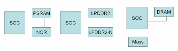
One of the most interesting slides that Floman presented at the JEDEC Mobile Forum, in my opinion, was an image that showed three processor/memory architectures for mobile phones.

The graphic looked like this:


The two architectures on the left are execute-in-place (XIP) architectures. The leftmost architecture employs pseudo-static RAM and NOR Flash as memory and executes operating-system code directly from the NOR Flash memory. The middle architecture replaces the pseudo-static RAM and NOR Flash memory with LPDDR2 SDRAM and LPDDR2-N Non-Volatile Flash memory. It’s still an execute-in-place architecture but the memory components are newer and deliver more performance with better capacity.

The architecture on the right is a shadowing architecture where the OS code is stored in a mass-storage device (NAND Flash memory) and the code is first transferred to DRAM and then executed. High-end smartphones use this architecture.


These architectural designs will hold unless a new type of memory with both fast read/write times and non-volatile storage become commercially available in the required capacities and the required cost per bit. If that happens, the smartphone will only need one memory type—perhaps that might be magnetic RAM (MRAM) or Memristor-based memory. But that’s not the situation today.

The best possible performance, said Floman, will come from Wide I/O DRAM while the UFS (Universal Flash Storage) standard appears to be poised to become the next commonly used storage medium for smartphone design. UFS “will be the next generation mass memory” for smartphones, said Floman.

All of this evolution has but a single purpose. “You will not buy your next phone from the same manufacturer unless it provides new functions,” Floman said as he concluded his keynote speech.

Wednesday, May 16, 2012

Intel Roadmap to 2015 and Beyond: 5nm Technology

Intel discussed roadmap to 2015 at their annual Investor meeting day on the 10th of May 2012 in Santa Clara.
Topic mentioned included the roadway to 5nm process, 450 mm wafers. See more below.

Ron


Intel Roadmap to 2015 and Beyond: 5nm Technology, Merrifield Mobile Processor, Microservers and More

http://www.cnx-software.com/2012/05/15/intel-roadmap-to-2015-and-beyond-5nm-technology-merrifield-mobile-processor-microservers-and-more/


Intel had their annual Investor meeting day on the 10th of May 2012 in Santa Clara where we would learn a few things about what's ahead for Intel and the semiconductor industry. Paul Otellini, Intel President and Chief Executive Officer, started the meeting by giving some numbers about Intel results and showing opportunities existing for cloud and data center, personal computing, mobile devices and intelligent systems (for automotive, retail and communications markets). One interesting point was the tremendous growth in data Intel expects from 2,500 Exabytes per year (7 EB/day) today to 8,000 Exabytes by 2015 which the majority of the growth lead by Big data. He also boasted about Intel technology advantage. For example, Intel introduced High-K Metal Gate technology in 2007 and competitor only got it in products last year (btw Samsung Exynos 5 uses HKMG). They recently introduced Tri-gate technology and they only expect competitors to catch up within 4 years. Finally one of the slide (see below) shows that Intel intends to be able to manufacture silicon using 10 to 5nm technology sometimes after 2015.


Intel Manufacturing Technology Road Map

The technology to achieve this feat is still at the fundamental research stage however. You can read the presentation (PDF) for more details.

Kirk Skaugen, General Manager of the PC Client Group, mainly talked about Ultrabooks which are high-performance, expensive (700 USD up) and thin notebooks. Intel Haswell Processor is designed to power Ultrabooks (in 2013) able to get 10 days of connected standby providing 20 times more efficiency than Intel iCore 5 device available in 2011. If you want to know more about the future for Intel based PC, Laptop and Ultrabook, you can read the presentation.

Diane Bryant, Vice President & General Manager of the Datacenter & Connected Systems Group, mainly talked about high end servers, but there is also a small section about microservers showing Xeon processors (Ivy Brigde) consuming 17W and the lower-end Atom Centerton SoC consuming a mere 6W. You can download the PDF presentation to know more about Intel datacenter and cloud solutions, customers and prospects.

Now let's move to smartphones and tablets with Hermann Eul & Mike Bell of Intel Mobile and Communications Group. They started by showing Intel technological know-how for mobile applications and Intel R&D commitment with over 3,000 engineer working on software for Windows, Linux (Intel is No. 2 contributor) and other operating systems, including 1,200 working on Android for mobile.

Then they gave some details about Atom Medfield processor, their first smartphone processor, which can be integrated into smartphones that support 8MPixel camera, 1080p video via HDMI and last 14 days on a single battery charge (using a 1460mA battery). They also mentioned Anandtech article showing Medfield based Lava XOLO X900 beats the competition in terms of performance (for some benchmarks) and matches the power consumption of existing smartphones.

They also showed their smartphone platform roadmap with processors for both the high end and lower end segments of the market.


Intel Smartphone Platform Roadmap

At the higher-end, we would get:
*Intel Atom Z2580 with Intel XMM 7160 LTE + 2X HSPA+ providing twice the performance of Medfield.
*Merrifield processor with XXM 7260 using 22nm manufacturing process.

and the lower-end:
*Intel Atom Z2000 @ 1GHZ with XMM 6265 (HSPA+)
*Intel Atom 6331 (22nm)

as well as future processors based on 14nm technology.
Intel also provided their tablet roadmap with Clover Trail 1.8 GHz 32nm processor (2012), Bay Trail 22nm processor (2013) and next generation processor (no name yet) using 14nm process (2014).

Have a look at the presentation for more information.

Brian Krzanich, Chief Operating Officer, gave a presentation about manufacturing and fabs which I would not normally mention in this blog, were it not for this slide:


Revenue per Company and Factory Cost Depending on Wafer Size


Currently, silicon Fabs use 200mm wafers which requires company to generate 3 to 5 billions in revenue to stay afloat representing all companies in the chart above (Elpida recently filled for bankruptcy before being bought by Micron). Now some companies starts to move to 300mm. A manufacturing site designed for this type of wafer requires 9 to 12 billions in revenues (shown in green above), but as it scales it becomes much more cost effective than a 200mm wafer Fab. That means that companies such as Freescale, NXP Broadcom and AMD would eventually have to go Fabless to survive, be bought or go bankrupt. After 2015, Fabs designed for 450mm wafer will start to show up (I'm pretty sure there is a mistake on the slide above and "300mm Fab" should read "450mm Fab"). This type of Fab requires 15 billions in revenues according to Intel, which would means that only 2 or 3 companies in the world, namely Intel, Samsung and possibly TSMC will be large enough to have manufacturing sites, unless companies such as Texas Instruments and Toshiba buy smaller players in the meantime.

If you are interested, you can check the PDF.

There were also two other presentations by the sales team and the CFO. You can listen to the webcast and access all the presentation slides on Intel Corporation 2012 Investor Meeting

Tuesday, May 15, 2012

Hynix Next Gen. NAND Flash

In December 2011, at the IEDM conference Hynix presented their version of the next generation of NAND flash (smaller than 20nm). Key developments presented: "A middle-1x nm design rule multi-level NAND flash memory cell (M1X-NAND) has been successfully developed for the first time.

1) Quad spacer patterning technology (QSPT) of ArF immersion lithography is used for patterning mid-1x-nm rule wordline (WL). In order to achieve high performance and reliability, several integration technologies are adopted, such as

2) advanced WL air-gap process,

3) floating gate slimming process, and

4) optimized junction formation scheme. And also, by using

5) new N±1 WL Vpass scheme during programming, charge loss and program speed are greatly improved."
See more details below.
Ron


A middle-1X nm NAND flash memory cell (M1X-NAND) with highly manufacturable integration technologies
 Joowon Hwang, Jihyun Seo, et al., Hynix Semiconductor Inc.
5/14/2012 3:21 PM EDT
 Editor’s note: This work was first presented at the 2011 IEEE International Electron Devices Meeting (IEDM) and appears here courtesy of the IEEE.

For more information about IEDM 2012 (San Francisco, CA; December 10-12), click here. A middle-1x nm design rule multi-level NAND flash memory cell (M1X-NAND) has been successfully developed for the first time.
1) Quad spacer patterning technology (QSPT) of ArF immersion lithography is used for patterning mid-1x-nm rule wordline (WL). In order to achieve high performance and reliability, several integration technologies are adopted, such as 2) advanced WL air-gap process, 3) floating gate slimming process, and 4) optimized junction formation scheme. And also, by using 5) new N±1 WL Vpass scheme during programming, charge loss and program speed are greatly improved. As a result, mid-1x-nm design rule NAND flash memories has been successfully realized.

The NAND flash memory cell has been scaled down to the 2x [1,2,3] and 2y nm [4] generations aggressively. As scaling down of a cell size, many serious scaling problems were caused in 2x and 2y nm generation, however they were solved or managed by process, device, and system solutions. For further scaling down beyond 2y nm, we face new scaling limitations such as patterning limitation of ArF immersion spacer patterning technology (SPT), more severe control gate (CG) poly-Si filling problems between floating gates (FGs), and high electric field and charge loss problem between WLs. This paper describes several new advanced processes and operation schemes to overcome these problems, as shown in Table 1. As a result, M1XNAND flash cell is successfully implemented with highly manufacturable integration technologies.

Table 1: Major issues and solution of mid-1x cell technology. M1X-NAND cell process Figure 1 shows the layout of M1X-NAND flash cells. The half pitch of WL is middle-1x nm. The BL contacts are formed staggered arrangement and a string has several dummy WLs. In order to pattern middle-1x nm design rule WLs, QSPT is intensively developed to overcome limitation of ArF immersion SPT. Figure 1: Layout of Mid-1x-nm NAND (M1X-NAND) string with dummy WLs. The half pitch of WL is mid-1x-nm. As shown in Figure 2, first patterns are formed by photolithography and the two times combination of previous formed pattern and spacer are formed final patterns. Figure 2: Schematic diagram of QSPT (Quad Spacer Patterning Technology) key fabrication steps. Two times spacer patterning is used to make mid-1x patterning. The WL critical dimension (CD) of QSPT, which plays a very important role of Vth distribution factor, is precisely controlled less than 1.5% uniformity (see figure 3). QSPT is successfully adopted for mid-1x-nm design rule NAND cell patterning. Figure 3: Location dependence of WL CD variation of QSPT gate patterned NAND string. WL CD is precisely controlled under 1.5% uniformity. Figure 4 shows cross-sectional TEM micrographs of M1X-NAND cell, (a) along WL-direction, and (b) along BL-direction. Figure 4: Cross-section TEM view of the cell, (a) along WL direction, (b) along BL direction. The CGs are well patterned with middle-1x nm half pitch. The floating gate slimming process can achieve the void-free filling of CG poly-Si and wider active area CD, which can obtain large cell current. An electrical depletion in CG poly-Si is greatly suppressed by this void-free process. As a result, BL interference is successfully improved 20% compared with conventional process (see figure 5). The CG CoSi height was selected reasonably to achieve optimized gate shape and decrease WL RC delay for improvement program performance. Figure 5: The simulated results of BL interference with FG slimming scheme. BL interference can be improved to 20%. Cell performance To suppress charge loss (Q-loss) between CG and neighbor FG due to lateral high electric field during program, we have adopted an advanced CoSi-based WL air-gap process that has an air-gap portion above 50% between WLs. As shown in Figure 6(a), the electric field between CG and neighbor FG can be reduced 20% by an advanced CoSi-base WL air-gap. However, reduction electric field by WL airgap is not sufficient to prevent charge loss perfectly because of scale-down issues at mid-1x-nm cell size. So N±1 WL bias control scheme were adopted within WL air-gap. As a result we can also reduce the electric field 15% additionally (see figure 6(a)). Figure 6: (a) Electric field between CG and neighbor FG during programming. (b) 3-D e-field simulation with programmed PV3 neighbor cell. The electric field at point A can be reduced by air-gap and N±1 WL bias control. Then the advanced air-gap and N±1 WL scheme can greatly alleviate charge loss between CG and neighbor FG by decreasing electric field, as shown in Figure 7. Furthermore, as shown Figure 8, PGM speed is improved by N±1 WL scheme, because FG potential of program cell increase by cross coupling effect between WL and neighbor FG. Figure 9 shows the cell coupling ratio with and without air-gap. Cell coupling ratio can be also improved by air-gap due to reducing capacitance of WL direction. Figure 7: Improvement of charge loss with N±1 WL bias control method. Charge loss is greatly decreased to ~300mV by applying Vpass+2V to neighbor N±1 WL. Figure 8: Improvement of PGM speed with N±1 bias control method. Figure 9: Cell coupling ratio as technology shrinkage. Read current reduction is also major issue because of higher bulk doping for suppressing short channel effects in mid-1x-nm cell transistors. A new advanced junction scheme of cell and select transistor is adopted to maximize read current and reduce leakage current in unselected block (see figure 10). Figure 10: Read current with/without select Tr. junction optimization. Read current can be improved by select Tr. junction optimization. Cell Vth Distribution Figure 11 shows cell Vth distributions for the multi-level M1X-NAND cells. The Vth distributions have normal shapes and are well separated to three MLC states. This result confirms that M1X-NAND cell technology can be applied for high density MLC. Figure 11: Three-level programmed Vth distributions of M1X-NAND cells. Vth distributions are well separated to three MLC states. A highly manufacturable mid-1x-nm NAND flash memory (M1X-NAND) has been developed with new integration technologies, such as QSPT, advanced WL air gap process, floating gate slimming process, and optimized junction formation scheme, to overcome scaling limits of mid-1x-nm technology. The excellent device characteristics and reliability are achieved successfully. And also, a new N±1 WL Vpass scheme during programming has been also adopted to overcome WL-to-WL high field issue. Then, we have demonstrated a middle-1x nm-generation NAND flash memory (M1X-NAND) with high performance and reliability. References 1 K. Prall, et al., “25nm 64Gb MLC Technology and Scaling Challenge,” IEEE IEDM Technical Digest, pp. 102-103, 2010. 2. C. Lee, et al., “A Highly Manufacturable Integration Technology for 27nm a and 3bit/cell NAND Flash Memory,” IEEE IEDM Technical Digest, pp. 98-101, 2010. 3. H. Shim, et al., “Highly Reliable 26nm 64Gb MLC E2NAND (Embedded -ECC & Enhanced-efficiency Flash Memory with MSP (Memory Signal Processing) Controller,” VLSI Symp. Technical Digest, pp. 216-217, 2011. 4. K. Lee, et al., “A Highly Manufacturable Integration Technology of 20nm Generation 64Gb Multi-Level NAND Flash Memory,” VLSI Symp. Technical Digest, pp. 70-71, 2011. About the authors This article was contributed by the Flash Device Development & Advanced Process Team, R&D Division, Hynix Semiconductor Inc. The authors include J. Hwang, J. Seo, Y. Lee, S. Park, J. Leem, J. Kim, T. Hong, S. Jeong, K. Lee, H. Heo, H. Lee, P. Jang, K. Park, Myungshik Lee, S. Baik, J. Kim, H. Kkang*, M. Jang*, J. Lee*, G. Cho, J. Lee, B. Lee*, H. Jang, S. Park, J. Kim*, S. Lee, S. Aritome, S. Hong and S. Park

Friday, May 4, 2012

Micron Technology Likely Winner, Buying Chipmaker Elpida Memory

"Micron likely winner in bidding for Japan's Elpida-NHK" as predicted with details by Businessweek in Feb. 27, 2012 (see below)


Ron Maltiel


Micron Biggest Winner as Elpida Bankruptcy Sidelines Rival Tech

http://www.bloomberg.com/news/2012-02-28/micron-biggest-winner-as-elpida-bankruptcy-sidelines-rival-tech.html


Micron Technology Inc. (MU) will probably emerge as the top winner from the bankruptcy ofElpida Memory Inc. (6665), whose filing yesterday sidelines the last Japanese maker of computer memory chips and gives rivals the chance to scoop up factories on the cheap.
Elpida filed for Japan’s biggest bankruptcy in two years after chip prices plunged and it failed to win a second government bailout. The elimination of a top maker of dynamic random access memory would give the rest of the industry more control over production, helping to ease the price swings that have left Micron unprofitable for six of the past 10 years.
The headquarters building of Micron Technology Inc. in Boise, Idaho. Micron shares jumped 7.7 percent yesterday amid speculation that the company, the fourth-largest DRAM maker, might seek to acquire some of Elpida’s plants. Photographer: Matthew Staver/Bloomberg
Elpida Memory Inc. memory chips are displayed in this arranged photograph in Tokyo, Japan. Photographer: Tomohiro Ohsumi/Bloomberg

Elpida’s creditors will look for ways to recoup losses through the sale of such assets as a plant in Hiroshima valued at $1 billion by Sanford C. Bernstein & Co. For potential buyers such as Micron, that price tag would be about a fifth of the cost of building a new equivalent facility. That would fit with Micron’s strategy of trying tobuy up capacity cheaply, rather than making acquisitions that outstrip the company’s $1.9 billion in cash and compel it to take on debt.

“Micron is clearly the winner,” said Dan Berenbaum, a New York-based analyst at MKM Partners LP. “Now it’s a question of how much does Micron pay for the assets.”

Micron shares jumped 7.7 percent yesterday amid speculation that the company, the fourth-largest DRAM maker, might seek to acquire some of Elpida’s plants. Dan Francisco, a spokesman for Boise, Idaho-based Micron, declined to comment.

Elpida has facilities that are responsible for about 18 percent of DRAM industry output, making it the No. 3 supplier. A push to take the plants offline or use them for other kinds of chips would help ease oversupply and stem industrywide losses.

Falling DemandThe computer-memory industry has been grappling with a decline in demand, brought on by a global consumer shift to smartphones and tablet computers, which need less memory and typically use a different type of chip.

Elpida’s troubles were exacerbated by DRAM prices falling below the cost of production. Industry sales last year dropped 26 percent to $29.2 billion, according to an estimate by Gartner Inc. That followed a 72 percent surge in 2010.

The Japanese chipmaker was the product of a 1999 merger between the memory businesses of NEC Corp. and Hitachi Ltd., which exited the industry.
‘Ten-Foot Pole’If Micron makes a bid for some DRAM facilities, Elpida’s creditors will get an offer that’s “tough to swallow,” because the U.S. company knows it’s not likely to face any competition, said Hans Mosesmann, an analyst at Raymond James & Associates Inc.

“Nobody else is going to touch DRAM with a ten-foot pole,” said Mosesmann, who has a “strong buy” rating on Micron shares. “Micron is very practical. They don’t want all of Elpida.”
Earlier this month, Micron’s management told Mosesmann and other analysts the company is monitoring events in Japan to see if there are opportunities. Executives declined to comment on whether Elpida is one of them and what the company might do.
“It just doesn’t feel like there’s going to be any fresh capital put into the DRAM business,” Micron President Mark Adams said in an interview on Feb. 9. “If we’re right, then the industry is mature enough that consolidation could make a lot of sense.”
Elpida has total debt of about $4 billion and has reported five straight quarters of losses. Micron, which has been making acquisitions and driving industry consolidation for more than 10 years, has about $1.95 billion of debt, approximately equal to its cash reserves. The company has a target range for its debt- to-capital ratio of 20 percent to 25 percent. Its current cash plus market capital of $8.4 billion give it a debt-to-capital ratio of about 18 percent, according to data compiled by Bloomberg.
Debt GuidelinesIf Micron stays within those guidelines -- giving it the latitude to borrow about another $500 million -- it’s not going to have enough leeway to buy its Japanese rival, said Daniel Amir, a San Francisco-based analyst at Lazard Capital Markets LLC.
“They probably won’t just buy out Elpida,” Amir said. “They are not willing to break the bank. It’s not like they’re going to spend $2 billion.”

Samsung Electronics Co., which dominates the memory-chip business and is the only consistently profitable company in the industry, has said it will concentrate on running its own business, making it an unlikely bidder for Elpida’s assets.
“Samsung is not going to come to their rescue,” said Raymond James’s Mosesmann.
Profit StruggleExcluding Samsung -- which is also the world’s second- largest maker of mobile phones and the biggest maker of liquid crystal displays -- DRAM makers have struggled to make money.
Matching supply with demand poses a constant challenge in the market for DRAM for personal computers, where plants take years to come online and can’t be shut down cheaply. With factories costing billions of dollars to build, companies such as Elpida have found themselves facing debts they have trouble repaying.
In six of the past 10 years, industry companies have spent more cash than their operations have generated. Even including Samsung, whose share price has more than tripled, memory makers as a group have lost 40 percent of their market value since October 2002.
If output from Elpida’s plants is slowed down or halted, all of its rivals will benefit as supply gets closer to demand and prices stabilize, according to Shawn Webster, an analyst at Macquarie Capital USA Inc.
“Any time a competitor is in distress, it’s a positive for everybody else,” said Webster. “If you pull supply offline, that could help everybody in the DRAM industry.

Micron CEOEarlier this month, Micron lost longtime Chief Executive Officer Steve Appleton, who died in a plane crash. Mosesmann and other analysts speculated that his death might slow any possible negotiations for industry consolidation, because Appleton had been the driving force behind previous transactions.

Micron, which got its start with an investment from local potato magnate J.R. Simplot, became one of the largest makers of computer memory when it bought the memory operations of Texas Instruments Inc. in 1998. Since then, it has acquired plants from Toshiba Corp., bought control of a Japanese joint venture, and formed partnerships with Taiwan’s Nanya Technology Corp. and Intel Corp. to secure access to more production.
In 2008, as Germany’s Qimonda AG headed for bankruptcy and sought investments, Micron bought out its interest in Inotera Memories Inc. (3474)Qimonda subsequently went out of business, and its chipmaking equipment was sold off.
Micron has also walked away from opportunities. In April 2002, it abandoned a transaction under which it would have acquired the memory operations of South Korea’s Hynix Semiconductor Inc., the second-largest DRAM maker, after the companies couldn’t agree on terms.
‘In No Rush’One way that Micron might consider a purchase of Elpida would be if it could get cheap financing for a transaction from Elpida’s creditors, which are facing the dilemma of knowing that restructuring the company’s debt wouldn’t be enough to make it competitive again, according to Betsy Van Hees, a San Francisco- based analyst at Wedbush Securities. Elpida needs more money to invest in making its production more efficient, she said.
When asked on Feb. 10 whether he would take Micron’s debt level above 25 percent of its capital to make an acquisition that would consolidate the industry, Chief Executive Officer Mark Durcan told analysts he was going to be “very careful about putting the company in a position where we’re not confident we can deal with any additional debt.”
Still, he would consider taking the debt ratio higher if there was a good enough opportunity, he said.