My expertise in semiconductors, process, and circuits have led to some really interesting places. Thanks for having me on your show Max for a fascinating
Showing posts with label chip expert. Show all posts
Showing posts with label chip expert. Show all posts
Monday, November 27, 2017

Monday, February 2, 2015
Samsung, Apple's iPhone, and Fabs Consolidation

The increasing cost of semiconductor
fabrication has led to consolidation of fabs over the last few years (see March
2012 Moore's Law End? (Next semiconductors gen. cost $10 billion).
At the same time Apple was facing the risk of
depending on a single semiconductor fabrication source ( Foundry Rankings (Including Samsungs' iPad, iPhone Breakdown).
It makes sense for Apple to diversify its
chip production as discussed below.
"KGI
Research predicted that Samsung would end up producing around 75 percent of the
A9 chips with Global Foundry manufacturing the rest...
Another
report from BusinessKorea .. Apple would be using Samsung almost exclusively
for manufacturing NAND flash storage, RAM and batteries for the upcoming iPhone
6s and the Apple Watch."
See also report of Apple's A9 production
using Samsung's 14nm FinFET made by both Samsung and GlobalFoundaries (Samsung-GlobalFoundries deal gives Apple’s chip production
greater flexibility
Another benefit for Apple is control of its
chips price supplied by using more than one vendor.
Ron
Insightful, timely, and accurate semiconductor consulting.
Semiconductor information and news at - http://www.maltiel-consulting.com/
Insightful, timely, and accurate semiconductor consulting.
Semiconductor information and news at - http://www.maltiel-consulting.com/
iPhone 7, iPad 2015 Specs News: Apple Seen Picking Samsung To Manufacture Most A9 Chips For New iPhones, iPads

YOUTUBE/APPLE
The A8 chip.
Rumors swirling around Apple's new devices in its iPhone and iPad ranges continue, with the latest concerning what type of chip will be used. All recent rumors pointed towards Samsung winning the contract to manufacture the bulk of the new A9 chips, which will be at the heart of the new iPhones and iPads.
Initially, it was reported that Taiwan Semiconductor Manufacturing Company had won the contract and would be manufacturing most of the A9 chips. However, soon after another report stated that instead of the Taiwan company, Samsung had been contracted to supply most of the A9 and A9X chips that would be used on the new iPhones and iPads.
With no official confirmation on the subject, speculations have increased on the company that would eventually produce the new Apple chip. In a recent statement, Samsung declined to provide any information, saying that "it does not comment on market speculation"
A report by KGI Research predicted that Samsung would end up producing around 75 percent of the A9 chips with Global Foundry manufacturing the rest. This report followed an earlier note by KGI Research that pointed towards Apple spreading out the production of the chip among the Taiwan semiconductor company, Samsung, Qualcomm, Global Foundry and Intel. It also hinted that Apple had tapped Samsung for manufacturing the S1 chips which will be featured in the upcoming Apple Watch. As for the Taiwan company, it will be more involved in producing the S2 chip which will be used in future versions of the Apple Watch.
Another report from BusinessKorea last month stated that Apple would be using Samsung almost exclusively for manufacturing NAND flash storage, RAM and batteries for the upcoming iPhone 6s and the Apple Watch.
While all these reports are speculations at this point, several research houses have noted that Apple is looking to engage many suppliers to produce the A9 chip in order to minimize any risks involved.
Thursday, December 4, 2014
3D Flash Race:Intel vs Samsung

Following Samsung development of V- NAND Intel introduce their
version of 3D NAND (see below). One of the benefits of 3D flash memories is the
capability of using larger design rules such as 30-40 nm instead of scaling the
design rules to smaller than 20nm.
One of the key problem of
shrinking to smaller design rules than 20nm is the cost and complexity of
multi-patterning photolithography and EUV lithography difficulties (ASML: Next-gen chipmaking tool ready forproduction in 2016 ). In addition, the reliability of the flash memory
degrades when the memory cells become too close to each other.
"Samsung consciously went
from a 24-layer 128Gbit MLC die to a 32-layer 86Gbit MLC die. In other words,
Samsung could have upped the die capacity to ~170Gbit by just adding the extra
layers, but the company chose to go with a smaller die instead. Smaller capacity
dies have advantages in performance (higher parallelism) and applicability
because eMMC/microSD devices have very strict die size constraints, "
Ron
Insightful, timely, and accurate semiconductor consulting.
Semiconductor information and news at - http://www.maltiel-consulting.com/
Intel's 3D NAND to Ship in H2'15: 256Gbit Die
& 32 Layers
by Kristian Vättö on November 25, 2014 5:20 AM EST
Last Thursday in its annual Investor Meeting Intel revealed the first details of its 3D NAND technology and announced that it will begin the shipments of 3D NAND in the second half of 2015. While Intel's investment in 3D NAND hasn't been a secret, the company has been relatively quiet about any specifics and the vital specs such as the number of layers and die capacity have remained unknown. In Thursday's webcast, Rob Crooke, Senior VP and General Manager of Intel's non-volatile memory group, disclosed that Intel's first generation 3D MLC NAND die will be 256Gbit (32GB) in capacity and will consist of 32 layers. The technology also enables a 384Gbit (48GB) TLC (3-bit-per-cell) die as we have learned over the years.
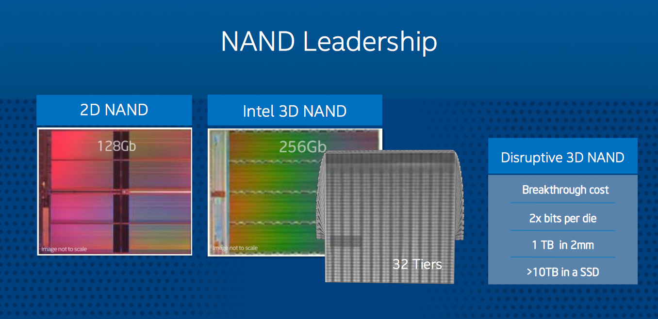
Intel claims that its 3D NAND is the most cost effective on the market and bases this on the fact that its die is 256Gbit whereas Samsung's is only up to 128Gbit at the moment. I'm not sure if I buy Intel's claim because while it's true that a higher capacity die results in higher array efficiency (i.e. peripheral circuitry takes less area), Samsung consciously went from a 24-layer 128Gbit MLC die to a 32-layer 86Gbit MLC die. In other words, Samsung could have upped the die capacity to ~170Gbit by just adding the extra layers, but the company chose to go with a smaller die instead. Smaller capacity dies have advantages in performance (higher parallelism) and applicability because eMMC/microSD devices have very strict die size constraints, so that might be a part of the reason why Samsung's strategy is so different from Intel's and Micron's.

As the graph above shows, Intel's/Micron's NAND dies have historically been larger than the competitors', so the die capacity alone isn't enough to dictate whether Intel's 3D NAND is more cost efficient than Samsung, especially because both have 32 layers. Unlike Samsung, Intel didn't reveal the lithography that is used to manufacture the 3D NAND, but I would say it's safe to assume that the lithography is in the order of 30nm or 40nm because the whole idea of 3D NAND is to move away from multi-patterning to cut costs and with today's technology the smallest pitch of single-patterning is somewhere between 30nm and 40nm. Either way, it will be very interesting to see how Intel's 3D NAND stacks up against Samsung's because there are also some structural differences that affect the production cost as well as performance and endurance, but I'll save the structural analysis for a future article.
Intel said that 3D NAND technology will enable +10TB SSDs in the 'next couple of years', but it wasn't clear whether that is with first generation 3D NAND or some later generation with more layers and higher die capacity. Currently Intel's lineup tops out at 2TB (P3700 & P3600) with a 128Gbit die, so the 256Gbit die alone isn't enough to bring the capacities above 10TB. With effective controller development it should certainly be possible to build a 10TB SSD with a 256Gbit die, although I'm still inclined to believe that Mr. Crooke was referring to second or third generation 3D NAND with his statement.
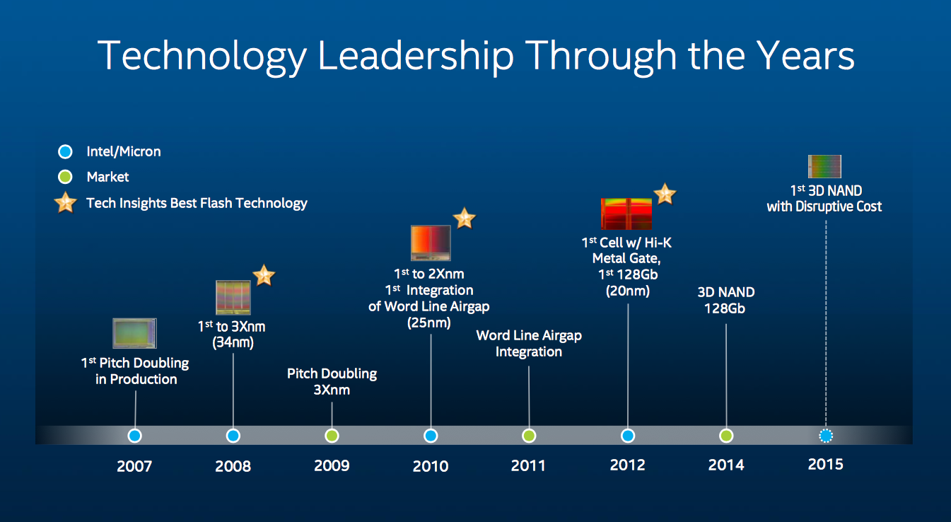
Similar to Intel's previous NAND efforts, 3D NAND has been jointly developed with Micron and will most likely be manufactured in the co-owned Utah plant as Intel sold its share in other fabs a couple of years ago. Interestingly enough, Mr. Crooke said that they also have the ability to bring 3D NAND production to an Intel fab, although to me that sounded more like a statement of technological possibility rather than a hint of future strategy. I wouldn't rule it out, though, but like Mr. Crooke said in the Q&A, Intel needs to have significant competitive advantage for it to make sense. In the past Intel's NAND technologies have generally been slightly ahead of the rest of the industry, but at least as of now Intel doesn't seem to have any substantial advantage in 3D NAND technology as Samsung is already shipping a 32-layer die and will likely ship a 48-layer die before Intel ships its 32-layer product.
All in all, we'll likely get more crumbs of information as the second half of 2015 gets closer. Given Intel's recent SSD strategy, I expect 3D NAND to first find its way to enterprise-class SSDs, but we'll see soon enough.
Wednesday, November 5, 2014
iPhone A8, A9 - Samsung or TSMC

Ron
Insightful, timely, and accurate semiconductor consulting.
Semiconductor information and news at - http://www.maltiel-consulting.com
Samsung and TSMC Reportedly Still Competing for Rights to Produce Apple's A9 Chip
Tuesday November 4,
2014 1:57 AM PST by Richard Padilla
Samsung and Taiwan Semiconductor Manufacturing Company
(TSMC) are still competing for the rights to produce Apple's next-generation A9
chip as a primary supplier is expected to be named by the end of this year, reports Digitimes.
According to the report, Samsung has offered Apple lower pricing quotes in an attempt to secure the rights to produce the A9. The company is also willing to produce other chips like flash memory and perform optimization services in-house. Samsung was the longtime producer of Apple's A-series chips until Apple struck a deal with TSMC to produce its chips last year.
Last month, Samsung semiconductor head Kim Ki-nam announced that the company would begin work on 14-nanometer processors for Apple, indicating that the Korean company may have already won the bid to produce the next-generation A9 chip. However, it is also possible that both companies could share the production load as Apple looks to diversify its supply chain even further to better fit its production needs.
Last year, it was reported that Apple signed a contract with Samsung to handle 30% to 40% of total A9 chip production, as TSMC would be handling the rest of the production load. Apple's A9 chip would presumably be featured in next year's line of iPhones and iPads, as the iPhone 6 and 6 Plus currently use the 20-nanometer A8 processor. The iPad Air 2 uses a more powerful triple-core A8X chip which is up to 55% faster than the A8 chip found in the iPhone 6.
According to the report, Samsung has offered Apple lower pricing quotes in an attempt to secure the rights to produce the A9. The company is also willing to produce other chips like flash memory and perform optimization services in-house. Samsung was the longtime producer of Apple's A-series chips until Apple struck a deal with TSMC to produce its chips last year.
Last month, Samsung semiconductor head Kim Ki-nam announced that the company would begin work on 14-nanometer processors for Apple, indicating that the Korean company may have already won the bid to produce the next-generation A9 chip. However, it is also possible that both companies could share the production load as Apple looks to diversify its supply chain even further to better fit its production needs.
Last year, it was reported that Apple signed a contract with Samsung to handle 30% to 40% of total A9 chip production, as TSMC would be handling the rest of the production load. Apple's A9 chip would presumably be featured in next year's line of iPhones and iPads, as the iPhone 6 and 6 Plus currently use the 20-nanometer A8 processor. The iPad Air 2 uses a more powerful triple-core A8X chip which is up to 55% faster than the A8 chip found in the iPhone 6.
Monday, March 17, 2014
Self Encrypting SSD (SED) to Rescue Security/ Privacy?

The article below discusses benefits of integrating encrypting in
the hardware.
"Samsung claims
that self-encrypting drives are the solutions to better security...can protect sensitive data better than software solutions
because self-encrypting SSDs automatically encrypt information as it's saved to
the drive.”
A key benefit of SED (Self Encrypting
Drive) is the automated process, which makes it difficult for human error leaving
the data vulnerable (see Missed Alarms, 40 Mil. Stolen Credit Card Numbers: Target Blew It). In addition, the additional security level of the
hardware on silicon chip increase the difficulty for anybody trying to access
the data.
Remaining issues in protecting the data:
Is there any way to replicate the encryption key stored on the
silicon chip?
Can a government or a malicious vendor duplicate the encryption and transmit it
through a back door?
Ron
Insightful, timely, and accurate semiconductor consulting.
Semiconductor information and news at - http://www.maltiel-consulting.com/
Semiconductor information and news at - http://www.maltiel-consulting.com/
Will Self-Encrypting Drives Help Stop Data Breaches?
Monday, January 13, 2014
Apple A8 (Next Processor Chip)

The article below (and at the link) provides general background about Apple’s
A8 competitive advantages. Key benefits can
be gleaned from Apples purchases of small companies (see September 2013 How
Apple Leverages its R&D) would be an easier implementation of;
·
Security features such as secure TouchID,
·
HDR photography,
·
face detection,
·
and iAds
Insightful, timely, and accurate semiconductor consulting.
Semiconductor information and news at - http://www.maltiel-consulting.com/
Jan. 10, 2014 4:33 PM ET
The move to 64-bit has been years in the making. But we did it
because we wanted to put desktop-class processing power in
the palm of people's hands. - Apple iPhone 5s design web page [emphasis added]
Monday, November 25, 2013
Xbox, PlayStation 4 $332 Manufacturing Cost

TechInsights Teardown (see below) shows that both vendors
used many similar parts to optimize their investment in the next generation of
gaming consoles.
Based on iFixit tear down I believe that the tear down has a
minor error that would add about $3 to Xbox cost of manufacturing due to the 8GB EMMC NAND flash being used instead of:
"Xbox One also has 4GB eMMC NAND flash, making the
non-volatile category US$3 higher for Xbox One"
"One interesting component is an 8GB chunk of eMMC NAND
flash memory, the purpose of which Microsoft discussed last month with
Eurogamer. In the words of Microsoft Technical Fellow Andrew Goossen:
We use it as a cache system-side to improve system response
and again not disturb system performance on the titles running underneath. So
what it does is that it makes our boot times faster when you're not coming out
of the sleep mode—if you're doing the cold boot. It caches the operating system
on there. It also caches system data on there while you're actually running the
titles and when you have the snap applications running concurrently. It's so
that we're not going and hitting the hard disk at the same time that the title
is. All the game data is on the HDD. We wanted to be moving that head around
and not worrying about the system coming in and monkeying with the head at an
inopportune time.”
Ron
Insightful, timely, and accurate semiconductor consulting.
Semiconductor information and news at -
http://www.maltiel-consulting.com/
Teardown.com compares PlayStation 4 vs. Xbox One
TechInsights has performed a Quick Turn Teardown of the Sony PlayStation 4 and the Microsoft Xbox One.
TechInsights Teardown shows that both vendors used many similar parts to optimise their investment in the next generation of gaming consoles.
While AMD came out as a big winner in the APU (integrated CPU and GPU) there are choice design differences around the both the processor design and the use of memory in each device.
The TechInsights bill of materials (BOM) for the Microsoft Xbox One amounts to US$331.00. Based on this – and when the estimated costs for the peripherals are included – TechInsights believes Microsoft will have a gross profit of approximately US$100.00 per console sold. This is far better than the US$43.00 Sony will make per complete unit.
Says Al Cowsky, Costing Director, TechInsights: “At the console level, the Xbox One is US$10 less expensive than the PS4. This is primarily due to a US$23 memory premium on the PS4, but it is offset by an US$11 cost premium on the Xbox One processor.
"The Xbox One also has 4GB eMMC NAND flash, making the non-volatile category US$3 higher for Xbox One, while the housings/mechanicals of the Xbox One add another US$4 premium over the PS4.
"The Xbox One also comes with a Kinect vision system in-box with an estimated cost of US$39. This is more than made up for by the US$100 list price premium. Likewise, PS4 has an optional vision system accessory available for a list price of US$60 (unit not costed at this time)”


Friday, November 22, 2013
Facebook: Flash Storage in Database

“With the advent of flash storage, we are starting to see newer applications that can access data quickly by managing their own dataset on flash instead of accessing data over a network. These new applications are using what we call an embedded database.
“… When database requests are frequently served from memory or from very fast flash storage, network latency can slow the query response time. Accessing the network within a data center can take about 50 microseconds, as can fast-flash access latency. This means that accessing data over a network could potentially be twice as slow as an application accessing data locally. “
Additional technical details at Under the Hood: Building and open-sourcing RocksDBMore about Facebook Propels SSD Flash Storage
Ron
Insightful, timely, and accurate semiconductor consulting.
Semiconductor information and news at - http://www.maltiel-consulting.com/Facebook’s latest open source effort: a flash-powereddatabase called RocksDB
by Derrick Harris
SUMMARY:
Facebook has open sourced a new embedded database called
RocksDB that’s meant to take advantage of all the performance flash has to
offer, from right on the application server. It might be a sign of best
practices to come.
Facebook is on an open source roll lately, and on Thursday announced its latest open source project — an embedded key-value store called RocksDB. The company uses it to power certain user-facing applications that would suffer too much from having to access an external database over the network and to eliminate the certain problems relating to non-fully utilized IO performance on flash storage devices.
Facebook database engineer Dhruba Borthakur describes the
design of and rationale behind RocksDB in some detail in a blog post, but the
biggest factor leading to its creation might be the emergence of relatively
inexpensive flash storage cards for servers (or, in Facebook’s case,
custom-built servers packed entirely with flash).
“With the advent of flash storage, we are starting to see
newer applications that can access data quickly by managing their own dataset
on flash instead of accessing data over a network. These new applications are
using what we call an embedded database.
“… When database requests are frequently served from memory
or from very fast flash storage, network latency can slow the query response
time. Accessing the network within a data center can take about 50
microseconds, as can fast-flash access latency. This means that accessing data
over a network could potentially be twice as slow as an application accessing
data locally. “
RocksDB was designed with these new hardware realities in
mind, so it can take full advantage of the IOPS potential of flash memory as
well as the computing power of many-core servers, Borthakur explains. Facebook
has posted the results of a benchmark test running on a Fusion-io-powered
server on the RocksDB GitHub page, and claims it’s significantly faster than
Google’s LevelDB embedded key-value store.
From a broader IT perspective, RocksDB signals that the
shifts in storage and computing economics that made the big data movement
possible are now making their way into web application development, albeit
using a storage media most organizations would consider using for storing “big
data.” Facebook is performance hungry, but it’s also cost-sensitive, and it
wouldn’t be storing “close to a petabyte of data across different
applications,” as Borthakur writes, if the cost to do so was out of control.
He offered a handful of application types an embedded
database like RocksDB is suitable for, including:
1. A user-facing application that stores the viewing history
and state of users of a website.
2. A spam-detection application that needs fast access.
3. A graph-search query that needs to scan a data set in
realtime.
4. RocksDB can be used to cache data from Hadoop, thereby
allowing an app to query Hadoop data in realtime.
5. A message-queue that supports a high number of inserts
and deletes.
In fact, Facebook has been finding all sorts of new ways to
utilize flash as stepping stone between slow disks on one hand and
expensive-but-fast RAM on the other.
Facebook is no doubt an early adopter of flash-heavy
application architectures, but it’s also probably serving as a guiding light
for other companies and their developers who want to achieve Facebook-like
performance. As flash prices continue to drop — and now that Amazon Web
Services is offering a whole suite of flash-backed instances on EC2 (the prices
of which should also drop) — it’s conceivable we’re approaching an era of
ever-better web and mobile applications that communicate with the network and
the hard drive as little as possible.
Monday, October 28, 2013
DDR4- Latest DRAM is Here

More about DDR4 at Why migrate to DDR4?
- "Improved capacity and performance scalability:
- Improved power efficiency:
- Improved reliability, availability and serviceability (RAS):
DDR4 SDRAM specification improves RAS is that DDR4 device supports command and address parity error detection, as well as recovery from parity error...supports a connectivity test mode, so that a system controller can test and detect connectivity faults without needing to go through DRAM initialization sequencing...The DDR4 register also provides enhanced RAS over the DDR3 register in that the DDR4 register can be configured to support command blocking upon detection of a parity error.."
It will still be awhile before DDR4 will replace DDR3.
Ron
Insightful, timely, and accurate semiconductor consulting.
Semiconductor information and news at - http://www.maltiel-consulting.com/
Kristin Lewotsky
10/17/2013 10:30 AM EDT
After seven years of development, JEDEC released the DDR4 DRAM standard (JESD79-4) last fall. The standards committee recognized the ever-increasing performance demands placed on memory and knew that a simple update wouldn't be enough.
The DDR4 architecture represents a major departure from that of previous DRAM standards, affording significant performance improvement, dramatic reductions in power demand, and compatibility with 3D architectures. Typically, a couple of years elapses between the release of a standard and broad availability of product.Given the rapid evolution of the technology, however, DDR4 is expected to mature quite a bit more rapidly than its predecessors, with broad deployment hitting in 2014. Indeed, at the recent Intel Developers Forum (IDF), companies demonstrated working systems, like Kingston Technology's memory demo highlighting 192 GB of working 2133 MT/s DDR4 Registered DIMMs at 1.2V operating on a future Intel reference platform. We thought it was a good time to take a look at some of the offerings out on the market available to design engineers.
The following slideshow reveals that the products curently sampling go beyond memory modules to include controllers and chipsets.
SDRAM controller and PHY (Altera)SDRAM controller and PHY (Altera)

A DDR4 SDRAM interface solution provides a flexible method for designers to interface external memory with FPGAs and SoCs. The Altera PHY megafunctions and associated High-Performance Memory Controller II (HPMCII) are two distinct offerings that can be used together or individually. The PHY megafunctions provide the interface between the memory controller and the external memory devices, performing read and write operations to memory. It can be used as part of the HPMCII MegaCore function to create a complete controller and PHY solution for DDR4 SDRAM, or they can be used separately with a custom controller.
DDR4 DRAM (Micron)DDR4 DRAM (Micron)

Micron's 8 Gb DDR4 DRAM operates at data rates as high as 2400 MT/s. By leveraging the power saving options enabled by the DDR4 standard, the devices deliver a 40 percent reduction in power consumption and 20 percent reduction in voltage compared to DDR3 DRAM. The components also sport a JTAG boundary scan feature to enable early fault detection during testing. At the 2013 Consumer Electronics Show, Micron's consumer line Crucial announced availability of DDR4 DRAM modules, although they do not appear currently on the company's website.
PHY IP (Synopsys)

A set of mixed-signal PHY IP cores provides a physical interface compliant to the DDR4 spec, as well as to LPDDR3 and prior editions. The Synopsys DesignWare DDR4 multiPHY IP supports DDR4 SDRAM speeds up to 2400 Mbps. Each DDR4 multiPHY encompasses an application-specific SSTL I/O library, a single address/command macro block, multiple-byte-wide data macro blocks instantiated as required to accommodate the memory channel width, and separate PLL macrocells that directly abut the address/command macro block and data macro blocks. They target 28-nm nodes and below.
Enterprise-class RDIMM (Innodisk)Enterprise-class RDIMM (Innodisk)

Innodisk a step toward the server market with the sampling of DDR4 RDIMMs. The family includes 4 GB, 8 GB, and 16 GB devices. Memory bus speeds start at 2133 MHz. With DDR4, the maximum capacity per chip has now been doubled from 64 GB to 128 GB. The higher memory densities possible with DDR4 will save space, simplify module construction, and improve internal airflow.
LRDIMM chipset (IDT)LRDIMM chipset (IDT)

This chipset for DDR4 RDIMMs and LRDIMMs combines IDT's 4DB0124 DDR4 data buffer and its 4RCD0124 registered clock driver (RCD) to provide complete buffering of command, address, clock, and data signals across an LRDIMM. Instantiating nine data buffers across the bottom of an LRDIMM with a single RCD in the center allows up to 16 ranks of DRAM to be reduced to a single load, minimizing stub lengths and physical skew between data bits and increasing the speed and bandwidth performance of LRDIMMs in multi-slot systems. The 4DB0124 supports advanced configuration and power interface (ACPI) states, which IDT claims reduces overall system power consumption.
DDR4 registering clock driver (Montage)DDR4 registering clock driver (Montage)

A dual-mode DDR4 registering clock driver (RCD) designed for next-generation server platforms can be used independently on an RDIMM or in conjunction with nine data buffers on an LRDIMM. With a variety of power-saving modes such as S3 low power mode, CK Stop mode, etc., the M88DDR4RCD01 from Montage Technology supports 1.2V VDD operations. It features a configurable 32-bit 1:2 registering buffer for address and control signals and I2C interface support.
DDR4 DRAM (Samsung)DDR4 DRAM (Samsung)

Samsung is taking aim at the enterprise server market with volume release of this family of 4 Gb DDR4 DRAM. Fabricated using 20-nm process technology, the devices deliver 2,667 Mbps operation, a factor of 1.25 greater than the company's 20-nm-class DDR3, all-consuming 30 percent less power. Current packaging includes a 78-ball BGA.
DDR4 register (Inphi)DDR4 register (Inphi)

A 0.95 JEDEC-compliant DDR4 register targeted at enterprise and IP data center supports up to DDR4-2666 memory. Inphi demonstrated its iDDR4RCD-GS02 at the Intel Developers' Forum, running a test system at speeds up to 2400 MT/s while consuming less power than DDR3-1866 modules of the same capacity. The register allows system designers to customize performance and power profile across a wider range of operating frequencies as compared to DDR3.
Subscribe to:
Posts (Atom)