Showing posts with label industrial. Show all posts

Monday, July 16, 2012

Flash NOR Memory Revival

NOR flash memory is being replaced by NAND in smart phones.  NOR, however, is finding new growth opportunities in tablets, automotive, and industrial computers as the article below discusses.  These new markets will help strengthen NOR's market share but it will not become as big as the NAND market.

Additional info is in my May 2007 article on Long Term Trends in the NOR and NAND Markets .


Ron


NOR Flash Makers Find New Growth Areas to Compensate for Slowing Sales in Cellphones, Teardown Results Reveal


July 13, 2012
http://www.isuppli.com/Memory-and-Storage/News/Pages/NOR-Flash-Makers-Find-New-Growth-Areas-to-Compensate-for-Slowing-Sales-in-Cellphones-Teardown-Results-Reveal.aspx
Ryan Chien


NOR flash memory sales growth may be tapering off in mobile handsets and smartphones, but lucrative embedded applications in the tablet, automotive and industrial markets are picking up the slack, according to the IHS iSuppli Storage Service at information and analytics provider IHS (NYSE: IHS).


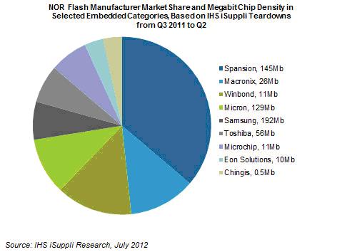
Based on a sample of 55 embedded products dissected by the IHS iSuppli Teardown Analysis Services over the course of three quarters, California-based Spansion Inc. led all NOR suppliers in terms of design wins. The company accounted for more than one-third of the NOR chips in the torn-down devices, as shown in the figure below.


Spansion, together with Samsung Electronics Co. Ltd. of South Korea and Micron Technology Inc. from Idaho, offered NOR chips in densities averaging in the hundreds of megabits. The three companies accounted for 53.4 percent of NOR chips in the three subsegments during the period from the third quarter of 2011 to the second quarter this year.


The rest of the market, equivalent to 46.6 percent of the sample, is controlled by companies that produced low-density NOR memory below the 100-megabit level. This group included big players like Taiwan’s Macronix International Co. Ltd. and Winbond Electronics Corp., as well as smaller entities like fellow Taiwanese firms Chingis Technology Corp. and Eon Silicon Solution Inc.


“Used to store small amounts of executable code, NOR flash was traditionally employed in devices like cellphones for fast read operations and random access capabilities,” said Ryan Chien, analyst for memory and storage at IHS. “However, newer implementations of NAND-based Embedded MultiMedia Card (eMMC) solutions that emulate NOR capabilities have resulted in NOR falling out of favor. The percentage of handsets using NOR flash has fallen from 14 percent in 2010 teardowns to less than 7 percent since then, found mostly in Samsung smartphones. However, NOR manufacturers have been proactive in their diversification efforts, borne out by a study of recent teardowns in both wireless and embedded categories.”


Tablets Energize NOR Market

Among the most prominent applications for NOR are tablets. Despite the elimination of NOR in the new iPad from Apple Inc., NOR chips were found in several Android alternatives in the teardowns, including the Eee Slate and Transformer Prime from Asus; the Jetstream and Flyer from HTC; and the Galaxy Tab 10.1 LTE and 7.7 from Samsung. Tablet devices from Samsung tended to incorporate the company’s own brand, higher-density NOR flash in multi-chip packages, while other branded tablets preferred discrete low-density SPI parts.


In the automotive space, NOR flash plays an increasing role to address vehicle safety regulations and manage user-comfort expectations. Head units in vehicles from Ford, General Motors, Nissan and Honda each had more than 230 megabits of NOR flash. NOR suppliers include Microchip and Micron for Honda and Toyota cars; Toshiba Corp. for Nissan vehicles; and Spansion for GM and Ford autos.


The other high-potential market for NOR flash is the industrial space. Network-attached storage systems from QNAP Systems and Buffalo Technology use Micron chips, and routers from Ubee Interactive and Ruckus Wireless each include 128 megabits of NOR.


An emerging industrial segment for NOR is the smart grid space, where devices such as feeder protection relays require high-density NOR to help monitor substation power lines. All of the NOR flash in hardware made by Sweden’s ABB Group is from Spansion, while solutions for U.S.-based Schweitzer Engineering Laboratories make use of Samsung and Spansion NOR parts. Samsung NOR is rare in third-party products, whereas Spansion has been aggressive in addressing this growth segment.


Wednesday, May 16, 2012

Intel Roadmap to 2015 and Beyond: 5nm Technology

Intel discussed roadmap to 2015 at their annual Investor meeting day on the 10th of May 2012 in Santa Clara.
Topic mentioned included the roadway to 5nm process, 450 mm wafers. See more below.

Ron


Intel Roadmap to 2015 and Beyond: 5nm Technology, Merrifield Mobile Processor, Microservers and More

http://www.cnx-software.com/2012/05/15/intel-roadmap-to-2015-and-beyond-5nm-technology-merrifield-mobile-processor-microservers-and-more/


Intel had their annual Investor meeting day on the 10th of May 2012 in Santa Clara where we would learn a few things about what's ahead for Intel and the semiconductor industry. Paul Otellini, Intel President and Chief Executive Officer, started the meeting by giving some numbers about Intel results and showing opportunities existing for cloud and data center, personal computing, mobile devices and intelligent systems (for automotive, retail and communications markets). One interesting point was the tremendous growth in data Intel expects from 2,500 Exabytes per year (7 EB/day) today to 8,000 Exabytes by 2015 which the majority of the growth lead by Big data. He also boasted about Intel technology advantage. For example, Intel introduced High-K Metal Gate technology in 2007 and competitor only got it in products last year (btw Samsung Exynos 5 uses HKMG). They recently introduced Tri-gate technology and they only expect competitors to catch up within 4 years. Finally one of the slide (see below) shows that Intel intends to be able to manufacture silicon using 10 to 5nm technology sometimes after 2015.


Intel Manufacturing Technology Road Map

The technology to achieve this feat is still at the fundamental research stage however. You can read the presentation (PDF) for more details.

Kirk Skaugen, General Manager of the PC Client Group, mainly talked about Ultrabooks which are high-performance, expensive (700 USD up) and thin notebooks. Intel Haswell Processor is designed to power Ultrabooks (in 2013) able to get 10 days of connected standby providing 20 times more efficiency than Intel iCore 5 device available in 2011. If you want to know more about the future for Intel based PC, Laptop and Ultrabook, you can read the presentation.

Diane Bryant, Vice President & General Manager of the Datacenter & Connected Systems Group, mainly talked about high end servers, but there is also a small section about microservers showing Xeon processors (Ivy Brigde) consuming 17W and the lower-end Atom Centerton SoC consuming a mere 6W. You can download the PDF presentation to know more about Intel datacenter and cloud solutions, customers and prospects.

Now let's move to smartphones and tablets with Hermann Eul & Mike Bell of Intel Mobile and Communications Group. They started by showing Intel technological know-how for mobile applications and Intel R&D commitment with over 3,000 engineer working on software for Windows, Linux (Intel is No. 2 contributor) and other operating systems, including 1,200 working on Android for mobile.

Then they gave some details about Atom Medfield processor, their first smartphone processor, which can be integrated into smartphones that support 8MPixel camera, 1080p video via HDMI and last 14 days on a single battery charge (using a 1460mA battery). They also mentioned Anandtech article showing Medfield based Lava XOLO X900 beats the competition in terms of performance (for some benchmarks) and matches the power consumption of existing smartphones.

They also showed their smartphone platform roadmap with processors for both the high end and lower end segments of the market.


Intel Smartphone Platform Roadmap

At the higher-end, we would get:
*Intel Atom Z2580 with Intel XMM 7160 LTE + 2X HSPA+ providing twice the performance of Medfield.
*Merrifield processor with XXM 7260 using 22nm manufacturing process.

and the lower-end:
*Intel Atom Z2000 @ 1GHZ with XMM 6265 (HSPA+)
*Intel Atom 6331 (22nm)

as well as future processors based on 14nm technology.
Intel also provided their tablet roadmap with Clover Trail 1.8 GHz 32nm processor (2012), Bay Trail 22nm processor (2013) and next generation processor (no name yet) using 14nm process (2014).

Have a look at the presentation for more information.

Brian Krzanich, Chief Operating Officer, gave a presentation about manufacturing and fabs which I would not normally mention in this blog, were it not for this slide:


Revenue per Company and Factory Cost Depending on Wafer Size


Currently, silicon Fabs use 200mm wafers which requires company to generate 3 to 5 billions in revenue to stay afloat representing all companies in the chart above (Elpida recently filled for bankruptcy before being bought by Micron). Now some companies starts to move to 300mm. A manufacturing site designed for this type of wafer requires 9 to 12 billions in revenues (shown in green above), but as it scales it becomes much more cost effective than a 200mm wafer Fab. That means that companies such as Freescale, NXP Broadcom and AMD would eventually have to go Fabless to survive, be bought or go bankrupt. After 2015, Fabs designed for 450mm wafer will start to show up (I'm pretty sure there is a mistake on the slide above and "300mm Fab" should read "450mm Fab"). This type of Fab requires 15 billions in revenues according to Intel, which would means that only 2 or 3 companies in the world, namely Intel, Samsung and possibly TSMC will be large enough to have manufacturing sites, unless companies such as Texas Instruments and Toshiba buy smaller players in the meantime.

If you are interested, you can check the PDF.

There were also two other presentations by the sales team and the CFO. You can listen to the webcast and access all the presentation slides on Intel Corporation 2012 Investor Meeting

Tuesday, May 15, 2012

Hynix Next Gen. NAND Flash

In December 2011, at the IEDM conference Hynix presented their version of the next generation of NAND flash (smaller than 20nm). Key developments presented: "A middle-1x nm design rule multi-level NAND flash memory cell (M1X-NAND) has been successfully developed for the first time.

1) Quad spacer patterning technology (QSPT) of ArF immersion lithography is used for patterning mid-1x-nm rule wordline (WL). In order to achieve high performance and reliability, several integration technologies are adopted, such as

2) advanced WL air-gap process,

3) floating gate slimming process, and

4) optimized junction formation scheme. And also, by using

5) new N±1 WL Vpass scheme during programming, charge loss and program speed are greatly improved."
See more details below.
Ron


A middle-1X nm NAND flash memory cell (M1X-NAND) with highly manufacturable integration technologies
 Joowon Hwang, Jihyun Seo, et al., Hynix Semiconductor Inc.
5/14/2012 3:21 PM EDT
 Editor’s note: This work was first presented at the 2011 IEEE International Electron Devices Meeting (IEDM) and appears here courtesy of the IEEE.

For more information about IEDM 2012 (San Francisco, CA; December 10-12), click here. A middle-1x nm design rule multi-level NAND flash memory cell (M1X-NAND) has been successfully developed for the first time.
1) Quad spacer patterning technology (QSPT) of ArF immersion lithography is used for patterning mid-1x-nm rule wordline (WL). In order to achieve high performance and reliability, several integration technologies are adopted, such as 2) advanced WL air-gap process, 3) floating gate slimming process, and 4) optimized junction formation scheme. And also, by using 5) new N±1 WL Vpass scheme during programming, charge loss and program speed are greatly improved. As a result, mid-1x-nm design rule NAND flash memories has been successfully realized.

The NAND flash memory cell has been scaled down to the 2x [1,2,3] and 2y nm [4] generations aggressively. As scaling down of a cell size, many serious scaling problems were caused in 2x and 2y nm generation, however they were solved or managed by process, device, and system solutions. For further scaling down beyond 2y nm, we face new scaling limitations such as patterning limitation of ArF immersion spacer patterning technology (SPT), more severe control gate (CG) poly-Si filling problems between floating gates (FGs), and high electric field and charge loss problem between WLs. This paper describes several new advanced processes and operation schemes to overcome these problems, as shown in Table 1. As a result, M1XNAND flash cell is successfully implemented with highly manufacturable integration technologies.

Table 1: Major issues and solution of mid-1x cell technology. M1X-NAND cell process Figure 1 shows the layout of M1X-NAND flash cells. The half pitch of WL is middle-1x nm. The BL contacts are formed staggered arrangement and a string has several dummy WLs. In order to pattern middle-1x nm design rule WLs, QSPT is intensively developed to overcome limitation of ArF immersion SPT. Figure 1: Layout of Mid-1x-nm NAND (M1X-NAND) string with dummy WLs. The half pitch of WL is mid-1x-nm. As shown in Figure 2, first patterns are formed by photolithography and the two times combination of previous formed pattern and spacer are formed final patterns. Figure 2: Schematic diagram of QSPT (Quad Spacer Patterning Technology) key fabrication steps. Two times spacer patterning is used to make mid-1x patterning. The WL critical dimension (CD) of QSPT, which plays a very important role of Vth distribution factor, is precisely controlled less than 1.5% uniformity (see figure 3). QSPT is successfully adopted for mid-1x-nm design rule NAND cell patterning. Figure 3: Location dependence of WL CD variation of QSPT gate patterned NAND string. WL CD is precisely controlled under 1.5% uniformity. Figure 4 shows cross-sectional TEM micrographs of M1X-NAND cell, (a) along WL-direction, and (b) along BL-direction. Figure 4: Cross-section TEM view of the cell, (a) along WL direction, (b) along BL direction. The CGs are well patterned with middle-1x nm half pitch. The floating gate slimming process can achieve the void-free filling of CG poly-Si and wider active area CD, which can obtain large cell current. An electrical depletion in CG poly-Si is greatly suppressed by this void-free process. As a result, BL interference is successfully improved 20% compared with conventional process (see figure 5). The CG CoSi height was selected reasonably to achieve optimized gate shape and decrease WL RC delay for improvement program performance. Figure 5: The simulated results of BL interference with FG slimming scheme. BL interference can be improved to 20%. Cell performance To suppress charge loss (Q-loss) between CG and neighbor FG due to lateral high electric field during program, we have adopted an advanced CoSi-based WL air-gap process that has an air-gap portion above 50% between WLs. As shown in Figure 6(a), the electric field between CG and neighbor FG can be reduced 20% by an advanced CoSi-base WL air-gap. However, reduction electric field by WL airgap is not sufficient to prevent charge loss perfectly because of scale-down issues at mid-1x-nm cell size. So N±1 WL bias control scheme were adopted within WL air-gap. As a result we can also reduce the electric field 15% additionally (see figure 6(a)). Figure 6: (a) Electric field between CG and neighbor FG during programming. (b) 3-D e-field simulation with programmed PV3 neighbor cell. The electric field at point A can be reduced by air-gap and N±1 WL bias control. Then the advanced air-gap and N±1 WL scheme can greatly alleviate charge loss between CG and neighbor FG by decreasing electric field, as shown in Figure 7. Furthermore, as shown Figure 8, PGM speed is improved by N±1 WL scheme, because FG potential of program cell increase by cross coupling effect between WL and neighbor FG. Figure 9 shows the cell coupling ratio with and without air-gap. Cell coupling ratio can be also improved by air-gap due to reducing capacitance of WL direction. Figure 7: Improvement of charge loss with N±1 WL bias control method. Charge loss is greatly decreased to ~300mV by applying Vpass+2V to neighbor N±1 WL. Figure 8: Improvement of PGM speed with N±1 bias control method. Figure 9: Cell coupling ratio as technology shrinkage. Read current reduction is also major issue because of higher bulk doping for suppressing short channel effects in mid-1x-nm cell transistors. A new advanced junction scheme of cell and select transistor is adopted to maximize read current and reduce leakage current in unselected block (see figure 10). Figure 10: Read current with/without select Tr. junction optimization. Read current can be improved by select Tr. junction optimization. Cell Vth Distribution Figure 11 shows cell Vth distributions for the multi-level M1X-NAND cells. The Vth distributions have normal shapes and are well separated to three MLC states. This result confirms that M1X-NAND cell technology can be applied for high density MLC. Figure 11: Three-level programmed Vth distributions of M1X-NAND cells. Vth distributions are well separated to three MLC states. A highly manufacturable mid-1x-nm NAND flash memory (M1X-NAND) has been developed with new integration technologies, such as QSPT, advanced WL air gap process, floating gate slimming process, and optimized junction formation scheme, to overcome scaling limits of mid-1x-nm technology. The excellent device characteristics and reliability are achieved successfully. And also, a new N±1 WL Vpass scheme during programming has been also adopted to overcome WL-to-WL high field issue. Then, we have demonstrated a middle-1x nm-generation NAND flash memory (M1X-NAND) with high performance and reliability. References 1 K. Prall, et al., “25nm 64Gb MLC Technology and Scaling Challenge,” IEEE IEDM Technical Digest, pp. 102-103, 2010. 2. C. Lee, et al., “A Highly Manufacturable Integration Technology for 27nm a and 3bit/cell NAND Flash Memory,” IEEE IEDM Technical Digest, pp. 98-101, 2010. 3. H. Shim, et al., “Highly Reliable 26nm 64Gb MLC E2NAND (Embedded -ECC & Enhanced-efficiency Flash Memory with MSP (Memory Signal Processing) Controller,” VLSI Symp. Technical Digest, pp. 216-217, 2011. 4. K. Lee, et al., “A Highly Manufacturable Integration Technology of 20nm Generation 64Gb Multi-Level NAND Flash Memory,” VLSI Symp. Technical Digest, pp. 70-71, 2011. About the authors This article was contributed by the Flash Device Development & Advanced Process Team, R&D Division, Hynix Semiconductor Inc. The authors include J. Hwang, J. Seo, Y. Lee, S. Park, J. Leem, J. Kim, T. Hong, S. Jeong, K. Lee, H. Heo, H. Lee, P. Jang, K. Park, Myungshik Lee, S. Baik, J. Kim, H. Kkang*, M. Jang*, J. Lee*, G. Cho, J. Lee, B. Lee*, H. Jang, S. Park, J. Kim*, S. Lee, S. Aritome, S. Hong and S. Park