Showing posts with label Smartphone. Show all posts

Wednesday, November 19, 2014

China Cell Phone Growth in 2014-5

The growth of NAND flash consumption in China is a strong indication of cell phone, tablet, and other mobile products future growth in China. The prediction in the article below of

"The proportion of China's overall NAND Flash usage relative to the world's NAND Flash output... expected to hit 20.6 per cent in 2014, and 30 per cent or more in 2015."


This prediction will depend on a very high growth in mobile products


Ron
Insightful, timely, and accurate semiconductor consulting.
Semiconductor information and news at - http://www.maltiel-consulting.com/


Mobile device space lifts memory market in China

Posted: 18 Nov 2014  
China has consumed about 4.789 billion DRAM chips and 3.518 billion NAND Flash chips from the 2Gb category this year, accounting for a respective 19.2 per cent and 20.6 per cent of the world's total DRAM and NAND Flash output. This highlights the country's increasing business potential as a result of the appeal China generates in terms of consumer device markets such as PC, smartphone and tablets, indicated DRAMeXchange, a research arm of TrendForce.
China's PC DRAM consumption is presently at about 15 per cent. Benefiting from domestic demand, Lenovo has managed to raise the scale of its business operations over the years, and is acquiring other companies as a means to boost its presence among first tier manufacturers. While the company is still competing fiercely with HP for top position in the PC market, its overall PC shipments are ahead of all of its other competitors. For 2015, DRAMeXchange predicted that Lenovo's market share will arrive at about 17 per cent. As has been the case with the other markets, mobile DRAM is expected to gradually replace PC DRAM as the mainstream in China given the country's growing smartphone and tablet sales. Aside from ZTE and Huawei, which are doing relatively well overseas, most China-based smartphone brands are expected to place their focus on the domestic market. Based on TrendForce's 2014 market statistics, China alone accounts for 28 per cent of mobile DRAM's overall bit demand. The importance of China's economic development to the entire DRAM industry is expected to become more apparent next year as that proportion rises to over 40 per cent.
As the NAND Flash manufacturing processes are advancing to under 1ynm, many NAND Flash applications including smartphone and tablet-based eMMCs and notebook-based SSDs are showing improved growth in the market. Competition among global OEM manufacturers, meanwhile, is starting to become more intense, with brands other than Apple and Samsung starting to make their way into the country's lucrative market. The level of China's NAND Flash consumption has managed to grow considerably over recent years due to Lenovo's rise to prominence, the above-average growth shown by China's emerging brands, and the improving standards of China's hardware designs. By the end of 2014, DRAMeXchange projects that the NAND Flash market's total value in China will reach up to $6.3 billion. The proportion of China's overall NAND Flash usage relative to the world's NAND Flash output, on the other hand, is expected to hit 20.6 per cent in 2014, and 30 per cent or more in 2015.

China's efforts over the years to transform from a manufacturing-based to consumption-based economy has been largely successful. Given the consistent growth in its economy and the country's rising wage levels, many of the productions in China are bound to be outsourced to other emerging countries. The Chinese government's present goal is to improve the country's outlook by implementing strategic policies that are aimed at enhancing its industrial capabilities. One such policy involves increasing the imports of semiconductor components such as smartphone CPU, AP, DRAM and NAND Flash, the combined value of which exceeds the value of China's imports for oil. In the future, it would be interesting to see whether Unisplendour Corp. Ltd's (UNIS) efforts to integrate resources from Spreadtrum Communications, RDA and Intel will be successful.
Due to the relatively high proportion of CPU, DRAM and NAND Flash components imported by China, the government policies that are implemented with regard to these three product categories may prove critical to the country's industries. A few days ago, the Chinese government announced a policy worth nearly $20 billion that involves mastering the technologies at the upper streams of the country's semiconductor supply chain and applying these technologies to mid to lower streams. The main purpose behind this is to enable the country's supply chains to be more integrated and to allow momentum in China's domestic industries to persist.

Wednesday, September 24, 2014

Apple's iPhone 6 A8 Teardown

Chipworks has been quick to teardown Apple's A8 processor, which is the secret sauce driving the new iPhone 6. Some details of the teardown are discussed below.

"Apple has spent quite a bit of die size on improving performance through more complex CPU and GPU architectures and miscellaneous feature additions."


A8 is fabricated on TSMC 20nm process while  A7 was manufactured on Samsung 28nm process. Shrinking the transistors gate to 20nm enables the CPU to operate faster. While limiting A8 to 4 GPU cores and not 6 help to reduce the new iPhone power.


Ron
Insightful, timely, and accurate semiconductor consulting.
Semiconductor information and news at - http://www.maltiel-consultin


Chipworks Disassembles Apple's A8 SoC: GX6450, 4MB L3 Cache & More

by Ryan Smith on September 23, 2014 1:00 PM EST

One of the more enjoyable rituals with Apple’s annual iPhone launch is the decapping, deconstruction, and photographing of the processor die at the heart of Apple’s newest SoC.  While we can learn a lot about the SoC from software, for some things there’s just no replacement for looking at the hardware itself and counting the functional blocks present. And this year, as in past years, the honor of being the first to tear apart the SoC goes to Chipworks.
For determining the layout of A8, Chipworks reached out to us to solicit our input on their die shot, and after some rounds of going back and forth we believe we’ve come to a solid determination of some of A8’s features and how it has been configured. So let's dive in.
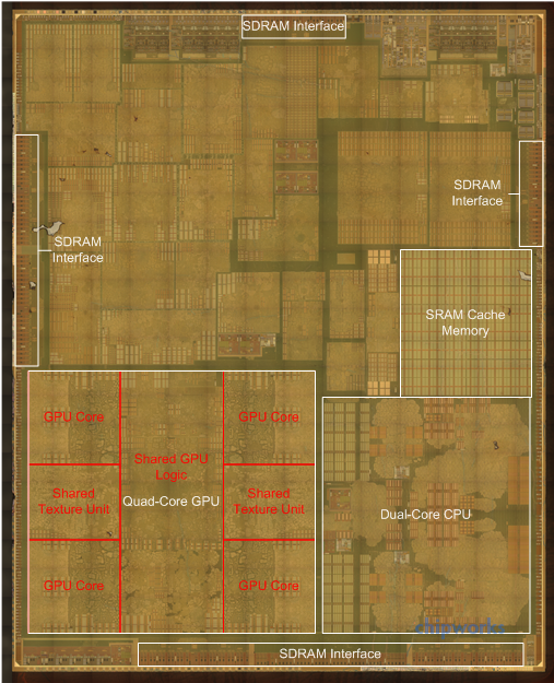
First and foremost we’ll start with A8’s GPU, as this was one of the hardest elements to analyze in software. Based on Apple’s 50% performance improvement we had previously speculated that A8 contained an Imagination PowerVR GX6650. However as we noted back then, a die shot would reveal all, and right on schedule it has.
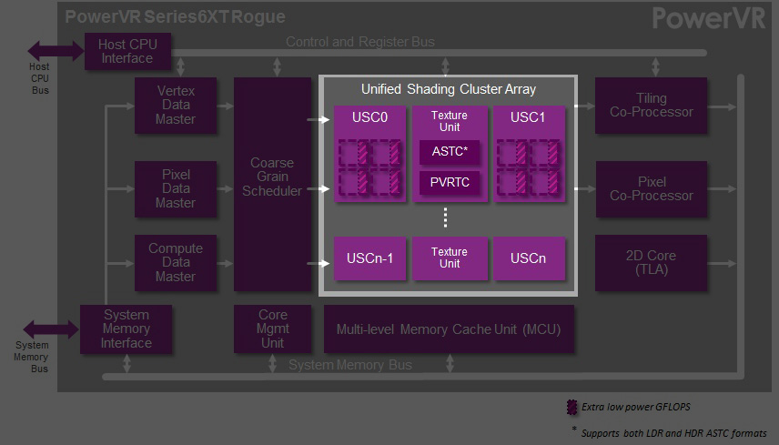
A close analysis of the die shot makes it clear that there are only 4 GPU cores available and not 6, which immediately rules out the 6 core GX6650 we were previously expecting. Instead with 4 cores present this is conclusive proof that Apple is using the smaller 4 core GX6450 on A8, the direct successor to the G6430 used on the A7. GX6450 induces some performance optimizations along with some feature updates – including ASTC support, which Apple’s documentation has already confirmed is present – so its inclusion here is a natural progression for Apple.
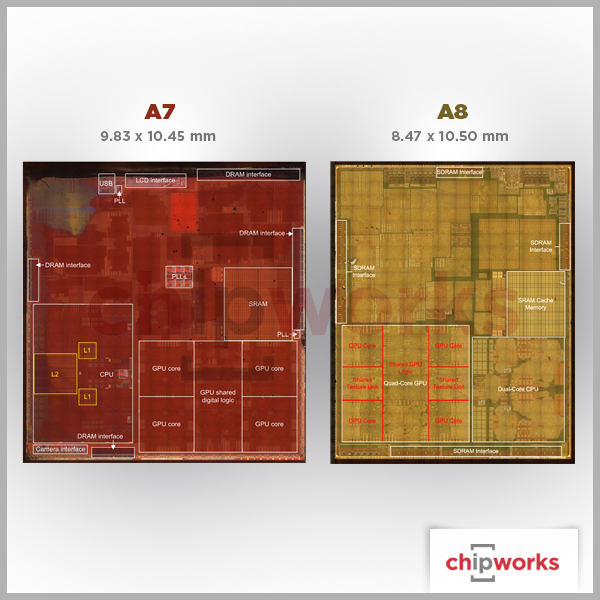
On A8 and its 20nm process this measures at 19.1mm2, versus A7’s 22.1mm2 G6430. As a result Apple is saving some die space compared to A7, but this is being partially offset by the greater complexity of GX6450 and possibly additional SRAM for larger caches on the GPU. Meanwhile looking at the symmetry of the block, it’s interesting that the blocks of texturing resources that every pair of GPU cores share is so visible and so large. With these resources being so big relative to the GPU cores themselves, you can see why Imagination would want to share them as opposed to building them 1:1 with the GPU cores.
Meanwhile opposite the GPU we have the CPU block. Unlike the GPU the CPU block has seen some significant shrinking, which Chipworks estimates is down from 17.1mm2 in A7 to 12.2mm2 in A8. In A7 Cyclone did not lend itself to easily picking apart the individual CPU cores, and neither does the CPU here in A8. We’ll be looking at the new CPU’s architecture in-depth in our iPhone 6 review, but for now it’s safe to say that while this is definitely derived from Cyclone, Apple has added a few tweaks over the last year that make it an even more potent CPU than the first Cyclone. Meanwhile based on this die shot Chipworks believes that the L2 cache has been reorganized to a per-core design, as there is no obvious single block of L2 on A8 like there was A7.

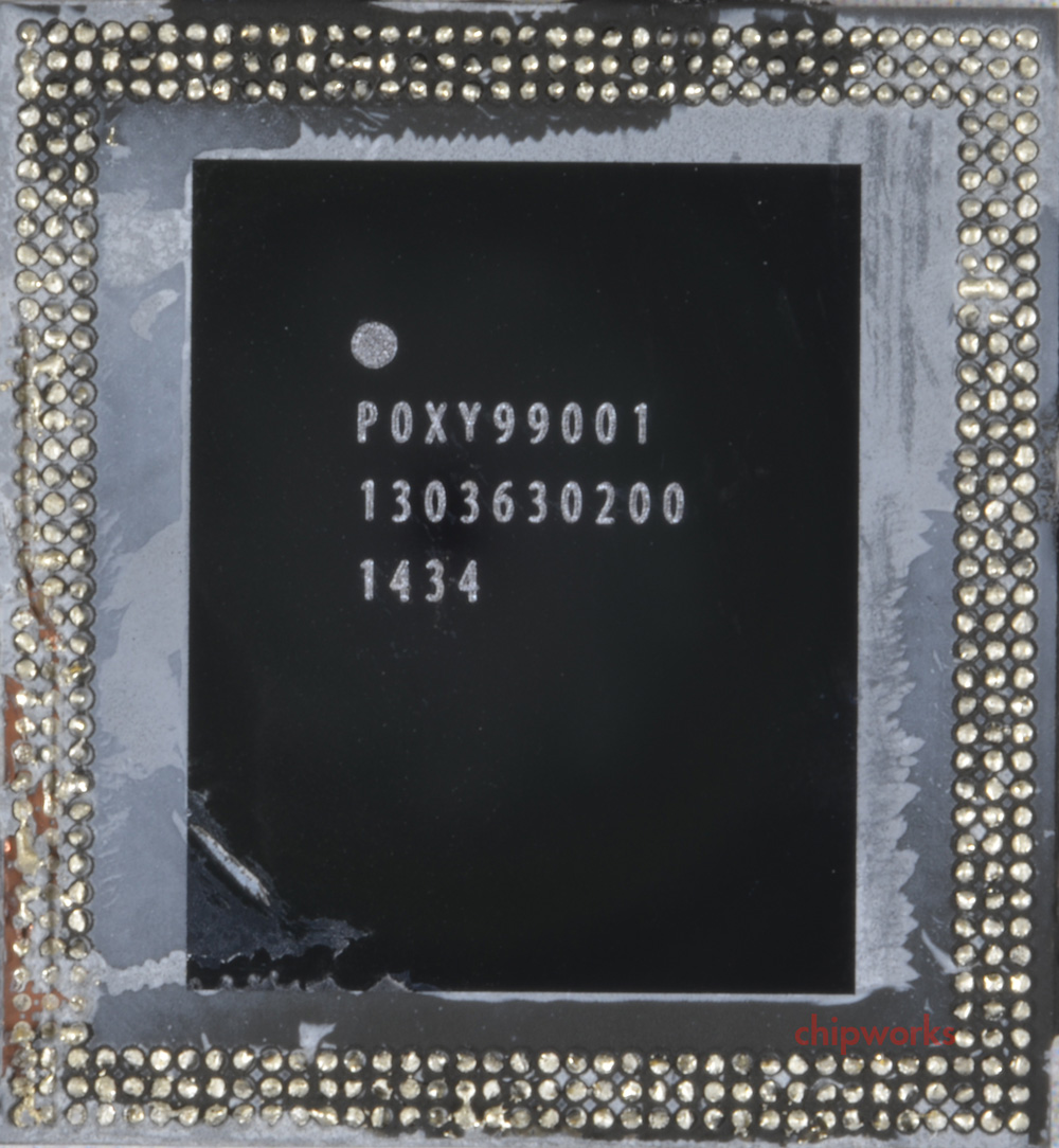
A8 With PoP DRAM Removed
The final major identifiable block on A8 is once again the SRAM cache memory. On A7 we discovered that this block was 4MB and was responsible for servicing the GPU and CPU. On A8 this block is similarly present and serving the same role. This 4MB of SRAM ends up being quite big despite the shrink from 28nm to 20nm, and while at first glance it seems like it should be larger than 4MB given the relative size, in practice what has happened is that the individual SRAM cells have not shrunk by a full 50%. Chipworks estimates the cell size to now be about 0.08µm2, versus 0.12µm2 on A7, which is closer to a 33% shrink that a 50% shrink. As a result the SRAM cache still takes up a fair bit of space, but the value of being able to serve larger memory requests without having to go off-die continues to be immense.
Apple A8 vs A7 SoCs
 Apple A8 (2014)Apple A7 (2013)
Manufacturing ProcessTSMC 20nm HKMGSamsung 28nm HKMG
Die Size89mm2104mm2
Transistor Count~2B"Over 1B"
CPU2 x Apple Enhanced Cyclone ARMv8 64-bit cores2 x Apple Cyclone ARMv8 64-bit cores
GPUIMG PowerVR GX6450IMG PowerVR G6430
Overall, Chipworks’ analysis points to A8 being fabbed on TSMC’s 20nm process. This makes A8 among the first SoCs to receive the 20nm treatment. Thanks to this smaller node Apple has been able to build in additional features to the SoC while simultaneously shaving off around 15% of their die size. Chipworks estimates the final die size of A8 to stand at 89mm2, versus the 104mm2 for the Samsung 28nm based A7. Chipworks notes that if this were a straight shrink that one would expect the A8 to be closer to 50% the size of A7 (though not all logic can shrink quite that well), which indicates that Apple has spent quite a bit of die size on improving performance through more complex CPU and GPU architectures and miscellaneous feature additions.
Wrapping things up, we’ll be back later this month with our review of the iPhone 6 family and our full analysis of the A8 SoC. So until then stay tuned.

Monday, August 18, 2014

Samsung, Apple, Xiaomi and China

Samsung face challenge due to lost business of Apple’s iPhones chips on one side (see October 2012 blog - Apple Cutting Out Samsung Chips )

While on the other side Samsung is squeezed by the rise of local cell phone vendors in china such as Xiaomi, Coolpad, Huawei, Lenovo, and ZTE (see Jan 2013 blog - Apples' Cook in China (MediaTek Impact). In addition see today's introduction of Xiaomi launches MIUI 6, makes Android look more like iOS 7

More on the fast rise of Xiaomi that "in the smartphone market in one of the world's biggest markets, research firm Canalys has revealed that Xiaomi was the market leader in its home territory of China, jumping ahead of Samsung for the first time in Q2 2014.
In the three months to the end of June, Xiaomi held a 14% market share in China with Samsung, Lenovo and CoolPad all trailing with 12% of the market while Huawei creeped into fifth spot with an 11% market share.


While it is not surprising to see Xiaomi at the top of the charts, the speed it has happened is surprising. In the first quarter of 2014, Samsung held an 18% market share while Xiaomi held just over 10%."  

Samsung respond by introducing a smartphone for china mobile as detailed in the article below.

Ron
Insightful, timely, and accurate semiconductor consulting.
Semiconductor information and news at - 
http://www.maltiel-consulting.com/


Samsung Launches Galaxy Win Pro Smartphone for China Mobile Powered by Marvell's ARMADA Mobile PXA1088 Quad-Core Platform 

February 18, 2014, 8:06 a.m. ET


Marvell's field-proven unified multi-core 3G mobile platform solution enables Samsung's latest world phone, the Galaxy Win Pro, to serve China Mobile's vast subscriber base with global WCDMA roaming capability

SANTA CLARA, Calif., Feb. 18, 2014 /PRNewswire/ -- Marvell (Nasdaq: MRVL) today announced the launch of the Galaxy Win Pro Smartphone for China Mobile powered by Marvell's ARMADA(R) Mobile PXA1088 Quad-Core Platform. Marvell's unified multi-core 3G mobile platform solution enables Samsung's Galaxy Win Pro, to serve China Mobile's vast subscriber base with global WCDMA roaming capability. The ARMADA Mobile PXA1088 single-chip platform is designed to drive high-quality and high-performance affordable solutions for mobile devices, furthering the "Smart Life and Smart Lifestyle." The Samsung Galaxy Win Pro is designed for China Mobile's expansive customer base and supports Global System for Mobile (GSM) and Time Division-Synchronous Code Division Multiple Access (TD-SCDMA) Wideband Code Division Multiple Access (WCDMA) to enable customers to have seamless Internet access regardless of location. With the Samsung Galaxy Win Pro, traveling is made easy for China Mobile's subscribers since they do not have to carry or lease extra 3G phones for global roaming with WCDMA/HSPA+.

"I am very proud to see the launch of Samsung's Galaxy Win Pro, quad-core-based mass-market smartphone for the world's largest mobile operator, China Mobile. Samsung's global leadership in delivering such affordable mobile devices with outstanding performance has enriched the lives of billions of consumers around the world through better communication and education," said Weili Dai, President and Co-Founder of Marvell. "I am very proud of our close collaboration with all key partners in the mobile ecosystem in driving the 'Smart Life and Smart Lifestyle.' I am very thankful to Samsung for their collaboration and dedication and thankful to Marvell's global teams of talented engineers for the passion, innovation and tireless effort to the successful launch of this great Galaxy smartphone."

The Samsung Galaxy Win Pro is a TD-SCDMA/GSM and W-CDMA/GSM dual-mode design that uses Marvell's all-in-one unified mobile computing platform, including wireless modem and RF transceiver that provide 3G world phone support. This enables the Samsung Galaxy Win Pro to be the choice of China Mobile's subscribers who needs to travel overseas. In addition to Marvell's ARMADA Mobile PXA1088, the Galaxy Win Pro also features the latest Marvell's RF839 3G radio transceiver, Marvell's advanced Avastar(R) 88W8777 IEEE802.11n Wi-Fi connectivity, and L2000 GPS. It also features a 4.5-inch qHD high resolution display, a 5MP camera and 8GB MLC storage with 1GB LPDDR2 memory.

About the Marvell ARMADA Mobile PXA1088:
The Marvell PXA1088 is a highly integrated quad-core application and communications mobile System-on-Chip (SoC) designed to provide high-performance, low-power mobile computing; support for all global broadband 3G standards, enabling seamless global roaming; and the latest wireless connectivity technology. Marvell's PXA1088 platform incorporates the performance of a quad-core ARM Cortex-A7 with Marvell's mature and field-proven cellular modem, including support for High Speed Packet Access Plus (HSPA+), Time Division High Speed Packet Access Plus (TD-HSPA+) and Enhanced Data for GSM Environment (EDGE). The PXA1088 enables a breakthrough end user experience for multimedia and gaming applications with universal connectivity. Marvell's complete mobile platform solution includes Marvell's advanced Avastar 88W8777 WLAN + Bluetooth 4.0 + FM single-chip SoC and the 88L2000 GNSS Hybrid Location Processor, and an integrated power management and audio codec IC. Marvell's unified mobile platform, includes the PXA986, PXA988, PXA1088 and PXA1088LTE, thus enabling easy migration from dual-core to quad-core solutions and support for TD-SCDMA, WCDMA and LTE.

Monday, August 26, 2013

Longest Battery Life Smartphone: Moto X (Teardown)

Below are some snapshot from Ifixit teardown of Google/ Motorola new cell phone. One of the key features of Motorola cell phones have been their very long battery life. Is it due to the combination of Qualcomm processor and the power management chip, some of the other chips, or their custom system architecture (software/ hardware)?

The key chips in Moto X are listed below.

Ron
Insightful, timely, and accurate semiconductor consulting.
Semiconductor information and news at -
http://www.maltiel-consulting.com/


Motorola Moto X Teardown

 
Image #1

Step 1 — Motorola Moto X Teardown 

  • The love child of Motorola and Google is here, and we are dying to crack open the little Motoroogle.
  • Technical Specifications:
    • Dual-core 1.7 GHz Qualcomm Snapdragon S4 Pro processor
    • 2 GB RAM
    • 4.7-inch 1280x720 pixels AMOLED display
    • 16 or 32 GB internal storage
    • Qualcomm Adreno 320 GPU
    • .........
    • Image #1

      Step 9 

      • Motorola claims the Moto X battery can power through an amazing 24 hours of "mixed usage."
      • How does the Moto X accomplish such a feat with a 3.8 volt, 2200 mAh Lithium ion battery? The secret is in the X8 Mobile Computing System.
      • The Motorola X8 Mobile Computing System is comprised of a Qualcomm Snapdragon S4Pro family processor, a natural language processor and a contextual computing processor.
      • Motorola developed a custom system architecture, which, when coupled with eight processor cores, allows for the delegation of processing power:
        • 4 graphics processor cores for "stunning clarity"
        • 2 application processor cores for "swift action"
        • 2 low-power cores—"awaiting your next command"
      Image #2

      Step 10 

      • Out comes the upper midframe panel, housing the speaker, headphone jack, more antennas, and pressure contacts.
        • Yay, pressure contacts! We like spring pressure contacts because they don't require any work to disconnect.
      • This is possibly the most modular headphone jack we've ever seen. It pops right out of the upper midframe panel, spring contacts and all.

      10 MP rear-facing camera

    • Image #1

      Step 15 

      • Notable ICs on the motherboard:
        • Toshiba THGBMAG7A2JBAIR 16 GB eMMC NAND Flash
        • SK Hynix H9TKNNNBPDAR RAM (we assume that the Snapdragon S4 Pro is also layered under this IC)
        • Qualcomm PM8921 Power Management IC
        • Texas Instruments TMS320C55 Digital Signal Processor
        • NXP 44701 NFC Chip
        • Skyworks 77619-12 Multiband Multimode Power Amplifier Module for Quad-Band GSM / EDGE and Penta-Band (Bands I, II, IV, V, VIII) WCDMA/ HSDPA/ HSUPA/ HSPA+/ LTE
        • Texas Instruments MSP430 F5259 Mixed Signal Microcontroller
      Image #1

      Step 16 

      • Additional ICs:
        • Qualcomm WCD9310 Audio Codec
        • Qualcomm WCN3680 802.11ac Combo Wi-Fi/Bluetooth/FM
        • NXP TFA9890 High Efficiency Class-D Audio Amplifier
        • Skyworks 77737 SkyHi™ Power Amplifier Module for LTE Bands 12/17 (698-716 MHz)
        • EPCOS 7 959 Wireless LAN / Bluetooth Filters (IF)
        • 0V00660 A56G 1B