Showing posts with label PC. Show all posts

Thursday, March 3, 2016

Semiconductor Startup Acquisition in 2016

Not only large semiconductor companies merge ( Update: China 2015/2016 Semiconductor Mergers, Acquisitions), startups are also acquired. Cisco acquisition of  Leaba semiconductor (see below) would help Cisco to lock up the network through their own chips. 

This purchase is similar to Apple snapping up semiconductor companies several years ago to strengthen future growth while See September 2013 blog - How Apple Leverages its R&D


Ron
Insightful, timely, and accurate semiconductor consulting.
Semiconductor information and news at - http://www.maltiel-consulting.com/


Cisco to acquire Leaba Semiconductor for $320 million as buying spree continues


By Ron Miller on March 2, 2016


Cisco continued its buying spree today as it announced its intention to acquire Israeli chip designer Leaba Semiconductor for $320 million.Cisco sees this acquisition as a way to bolster its hardware catalog with highly advanced chip technology.

“By combining Leaba’s semiconductor expertise with the Cisco engineering team, we will accelerate our plans for Cisco’s next generation product portfolio and bring new capabilities to the market faster,” Rob Salvagno, head of Cisco’s M&A and venture investing team wrote in a blog post announcing the purchase.

When the deal closes, the Leaba team will report to Core Hardware Group, led by Cisco senior vice president, Ravi Cherukuri, according to the blog post.

The company actually doesn’t even have a shipping product yet, R Ray Wang, founder at Constellation Research told TechCrunch. “They haven’t even finished their prototype. This is an acqui-hire for next generation semi-conductor [technology]. Think networking at the chip level,” he said.

This is not the first time the Leaba founding team has launched and sold a cutting edge chip production company, according to report in Globes, an Israeli business publication. The founding team, which consists of CEO Eyal Dagan and CTO Ofer Eini sold Dune Networks to Broadcom for $178 million in 2009.

Today’s news comes just the day after the company announced it was buying CliQr, a cloud hybrid services management platform for $260 million and just about a month after it bought Jasper Technologies for $1.4 billion.

Cisco is walking a fine transformational line here. On one hand, the purchase pattern suggests that the company is trying to pivot from its networking hardware roots to a business centered around services as the CliQr and Jasper Technologies would suggest.

Much like IBM, Cisco is looking to the future and trying to use its cash hoard to make strategic purchases to help speed up that transition.
At the same time, it’s not quite ready to give up completely on its hardware roots and purchasing a leading-edge semiconductor company suggests that it is still looking to a future where it can continue to lead in the networking hardware space.

Wednesday, November 19, 2014

China Cell Phone Growth in 2014-5

The growth of NAND flash consumption in China is a strong indication of cell phone, tablet, and other mobile products future growth in China. The prediction in the article below of

"The proportion of China's overall NAND Flash usage relative to the world's NAND Flash output... expected to hit 20.6 per cent in 2014, and 30 per cent or more in 2015."


This prediction will depend on a very high growth in mobile products


Ron
Insightful, timely, and accurate semiconductor consulting.
Semiconductor information and news at - http://www.maltiel-consulting.com/


Mobile device space lifts memory market in China

Posted: 18 Nov 2014  
China has consumed about 4.789 billion DRAM chips and 3.518 billion NAND Flash chips from the 2Gb category this year, accounting for a respective 19.2 per cent and 20.6 per cent of the world's total DRAM and NAND Flash output. This highlights the country's increasing business potential as a result of the appeal China generates in terms of consumer device markets such as PC, smartphone and tablets, indicated DRAMeXchange, a research arm of TrendForce.
China's PC DRAM consumption is presently at about 15 per cent. Benefiting from domestic demand, Lenovo has managed to raise the scale of its business operations over the years, and is acquiring other companies as a means to boost its presence among first tier manufacturers. While the company is still competing fiercely with HP for top position in the PC market, its overall PC shipments are ahead of all of its other competitors. For 2015, DRAMeXchange predicted that Lenovo's market share will arrive at about 17 per cent. As has been the case with the other markets, mobile DRAM is expected to gradually replace PC DRAM as the mainstream in China given the country's growing smartphone and tablet sales. Aside from ZTE and Huawei, which are doing relatively well overseas, most China-based smartphone brands are expected to place their focus on the domestic market. Based on TrendForce's 2014 market statistics, China alone accounts for 28 per cent of mobile DRAM's overall bit demand. The importance of China's economic development to the entire DRAM industry is expected to become more apparent next year as that proportion rises to over 40 per cent.
As the NAND Flash manufacturing processes are advancing to under 1ynm, many NAND Flash applications including smartphone and tablet-based eMMCs and notebook-based SSDs are showing improved growth in the market. Competition among global OEM manufacturers, meanwhile, is starting to become more intense, with brands other than Apple and Samsung starting to make their way into the country's lucrative market. The level of China's NAND Flash consumption has managed to grow considerably over recent years due to Lenovo's rise to prominence, the above-average growth shown by China's emerging brands, and the improving standards of China's hardware designs. By the end of 2014, DRAMeXchange projects that the NAND Flash market's total value in China will reach up to $6.3 billion. The proportion of China's overall NAND Flash usage relative to the world's NAND Flash output, on the other hand, is expected to hit 20.6 per cent in 2014, and 30 per cent or more in 2015.

China's efforts over the years to transform from a manufacturing-based to consumption-based economy has been largely successful. Given the consistent growth in its economy and the country's rising wage levels, many of the productions in China are bound to be outsourced to other emerging countries. The Chinese government's present goal is to improve the country's outlook by implementing strategic policies that are aimed at enhancing its industrial capabilities. One such policy involves increasing the imports of semiconductor components such as smartphone CPU, AP, DRAM and NAND Flash, the combined value of which exceeds the value of China's imports for oil. In the future, it would be interesting to see whether Unisplendour Corp. Ltd's (UNIS) efforts to integrate resources from Spreadtrum Communications, RDA and Intel will be successful.
Due to the relatively high proportion of CPU, DRAM and NAND Flash components imported by China, the government policies that are implemented with regard to these three product categories may prove critical to the country's industries. A few days ago, the Chinese government announced a policy worth nearly $20 billion that involves mastering the technologies at the upper streams of the country's semiconductor supply chain and applying these technologies to mid to lower streams. The main purpose behind this is to enable the country's supply chains to be more integrated and to allow momentum in China's domestic industries to persist.

Tuesday, September 10, 2013

How Apple Leverages its R&D

11 Apple products which were realised via strategic acquisitions
Apple leverages its R&D by buying 11 small companies over the last few years as is discussed in the article below.

For example,
"In 2010, Apple unveiled the first iPad. Inside of it was a powerful custom SoC designed by Apple called the A4. Later came the A5, A5X, A6, A6X, ....none of these outstanding SoCs would even be possible if Apple didn’t make a handful of strategic acquisitions over the last few years. In 2008, Apple picked up P.A. Semi ..., 2010 saw the acquisition of Intrinsity for ..., and Passif Semiconductor was purchased earlier this year"

See Apple iPad 4 – A6X teardown


Flash NAND is remaking computers, servers, mobile tablets, and cell phones architecture and Apple realizes it.

 "Anobit Technologies was founded in Israel in 2006. It developed dozens of patents for flash controllers,...Apple uses so many NAND chips in iPads, iPhones, iPods, and Macs, ...Apple acquired ... in December 2011 ... Any competitive edge Apple can find for creating cheaper and better flash-based devices holds the potential to drastically change its production chain. Flash storage is constantly improving, and it’s in Apple’s best interest to stay on the cutting edge of speed and reliability improvements."

HDR photography, face detection, and iAds  will be integrated in future Apple products (see below).

 Ron

Insightful, timely, and accurate semiconductor consulting.
Semiconductor information and news at -
http://www.maltiel-consulting.com/


11 Apple products which were realised via strategic acquisitions

 by Grant Brunner, 09 Sep 2013Features
Apple is widely thought of as a major innovator in the tech industry. While it’s true that Cupertino does employ some of the best designers and engineers in the world, Apple simply wouldn’t be where it is without a large number of strategic acquisitions. Most notably, iOS and OS X wouldn’t even exist without the purchase of NeXT.
Of course, that acquisition also brought Steve Jobs back to Apple, but that serves to highlight the strength of a smart acquisition. Not only will purchasing a company net you products and patents, but you’re gaining an influx of amazing employees as well.
In this article, I’d like to walk through a number of important acquisitions Apple has made in the last decade. From the A6 SoC through multitouch displays to Siri, Apple has relied heavily on acquired technology to build the iPhone, iPad, and iOS. It’s important to remember that purchases like these help make Apple what it is, and even the best engineers in the world need some fresh ideas from time to time.

Multitouch

FingerWorks, founded by doctoral students at the University of Delaware, focused on developing numerous devices like the TouchStream multitouch keyboard. Its quirky products never took off on a large scale, but the core technology and patents were successful enough to garner the attention of Apple. In 2005, Apple purchased the company, and effectively shut down the existing business. Two years later, the iPhone came out, and heavily featured multitouch technology.

Even if Apple was working on multitouch devices before the acquisition, it’s clear that the expertise and patent portfolio that came along with FingerWorks helped make multitouch displays become an industry standard.


App Store Genius

Chomp was founded in 2009, and served as a search engine for iOS and Android apps. The search tool was available on the web and as an app, and it enabled users to discover new and relevant apps more easily than Apple or Google’s built-in search engines. It received millions of dollars of venture capital funding, and even partnered with Verizon to build a backend for the telecom’s app store. Despite its success as an independent company, Apple was able to snatch up Chomp in early 2012 for a reported $50 million (£32 million). The Android and iOS apps disappeared, and the Chomp technology appears to be powering app searches and the App Store Genius functionality currently featured on the App Store.

Custom SoCs

In 2010, Apple unveiled the first iPad. Inside of it was a powerful custom SoC designed by Apple called the A4. Later came the A5, A5X, A6, A6X, and the rumoured upcoming A7 chip. However, none of these outstanding SoCs would even be possible if Apple didn’t make a handful of strategic acquisitions over the last few years. In 2008, Apple picked up P.A. Semi for $280 million (£180 million), 2010 saw the acquisition of Intrinsity for $121 million (£77 million), and Passif Semiconductor was purchased earlier this year for an unknown figure. With this ever increasing pool of talent and patents, Apple continues to make a name for itself in the world of SoC design.


Apple Maps

Apple’s maps have been a bit of a sore spot for the last year. Apple’s contract with Google ran out, and Apple decided to build its own solution. Of course, a few purchases helped get the ball rolling. Placebase was purchased back in July of 2009, Poly9 was added to Apple’s portfolio in July of 2010, and 3D mapping company C3 Technologies was acquired in August of 2011. This amalgam of purchases, alongside partnerships with companies like TomTom, led to the launch of Apple’s own mapping service in 2012. It was received very poorly, but Apple hasn’t stopped trying. WiFiSlam was purchased in March of this year, Locationary and HopStop.com were picked up in July, and Embark was snatched up by Cupertino just a couple of weeks ago. With this much mapping prowess under its roof, Apple is clearly taking this problem very seriously.

Flash storage

Anobit Technologies was founded in Israel in 2006. It developed dozens of patents for flash controllers, and quickly gained substantial notoriety and venture funding. Since Apple uses so many NAND chips in iPads, iPhones, iPods, and Macs, it was no surprise when Apple acquired the Israeli company and its patent portfolio in December 2011 for a whopping $390 million (£250 million). Any competitive edge Apple can find for creating cheaper and better flash-based devices holds the potential to drastically change its production chain. Flash storage is constantly improving, and it’s in Apple’s best interest to stay on the cutting edge of speed and reliability improvements.


HDR photography

Apple introduced built-in HDR (High Dynamic Range) photography on the iPhone 4 with the release of iOS 4.1. By taking multiple photos at different exposures, and then merging the visual data together, photographers can end up with better looking pictures with more detail in dark and bright areas. To help improve the core technology, Apple purchased a UK-based company called IMSense for an undisclosed amount of money in September 2010. As the hardware and software of the iPhone have improved, so have the overall quality of HDR images. Now, amazing HDR techniques are available to even novice photographers using iPhones.


Face detection

Faces might just be the most important part of personal photos. Finding and identifying faces is vital for good photography software, and Apple does a decent job on most fronts. iPhoto automatically finds faces, and attempts to guess who is in each photo based on previous input. On iOS, the camera app automatically detects faces, and enables developers to easily implement live photo manipulation. Part of this clever face detection is thanks to the 2010 acquisition of a Swedish company called Polar Rose. With that core technology, any developer on iOS can take advantage of automatic face detection thanks to the built-in Core Image API.


iAds

After Google began to make serious moves against Apple in the smartphone market, Cupertino decided to get into the advertising game – seemingly in retaliation towards its former partner. After a bit of a bidding war, Google was able to secure the purchase of AdMob in 2009. Not to be outdone, Apple purchased Quattro Wireless in 2010 to compete directly against Mountain View. iAds was born out of this purchase, although it never really took off on a large scale. Even so, this acquisition remains a notable point in the fascinating breakdown of the working relationship between Google and Apple.


Read more: http://www.itproportal.com/2013/09/09/11-apple-products-which-were-realised-via-strategic-acquisitions/#ixzz2eUrfkP4e

Monday, August 26, 2013

Longest Battery Life Smartphone: Moto X (Teardown)

Below are some snapshot from Ifixit teardown of Google/ Motorola new cell phone. One of the key features of Motorola cell phones have been their very long battery life. Is it due to the combination of Qualcomm processor and the power management chip, some of the other chips, or their custom system architecture (software/ hardware)?

The key chips in Moto X are listed below.

Ron
Insightful, timely, and accurate semiconductor consulting.
Semiconductor information and news at -
http://www.maltiel-consulting.com/


Motorola Moto X Teardown

 
Image #1

Step 1 — Motorola Moto X Teardown 

  • The love child of Motorola and Google is here, and we are dying to crack open the little Motoroogle.
  • Technical Specifications:
    • Dual-core 1.7 GHz Qualcomm Snapdragon S4 Pro processor
    • 2 GB RAM
    • 4.7-inch 1280x720 pixels AMOLED display
    • 16 or 32 GB internal storage
    • Qualcomm Adreno 320 GPU
    • .........
    • Image #1

      Step 9 

      • Motorola claims the Moto X battery can power through an amazing 24 hours of "mixed usage."
      • How does the Moto X accomplish such a feat with a 3.8 volt, 2200 mAh Lithium ion battery? The secret is in the X8 Mobile Computing System.
      • The Motorola X8 Mobile Computing System is comprised of a Qualcomm Snapdragon S4Pro family processor, a natural language processor and a contextual computing processor.
      • Motorola developed a custom system architecture, which, when coupled with eight processor cores, allows for the delegation of processing power:
        • 4 graphics processor cores for "stunning clarity"
        • 2 application processor cores for "swift action"
        • 2 low-power cores—"awaiting your next command"
      Image #2

      Step 10 

      • Out comes the upper midframe panel, housing the speaker, headphone jack, more antennas, and pressure contacts.
        • Yay, pressure contacts! We like spring pressure contacts because they don't require any work to disconnect.
      • This is possibly the most modular headphone jack we've ever seen. It pops right out of the upper midframe panel, spring contacts and all.

      10 MP rear-facing camera

    • Image #1

      Step 15 

      • Notable ICs on the motherboard:
        • Toshiba THGBMAG7A2JBAIR 16 GB eMMC NAND Flash
        • SK Hynix H9TKNNNBPDAR RAM (we assume that the Snapdragon S4 Pro is also layered under this IC)
        • Qualcomm PM8921 Power Management IC
        • Texas Instruments TMS320C55 Digital Signal Processor
        • NXP 44701 NFC Chip
        • Skyworks 77619-12 Multiband Multimode Power Amplifier Module for Quad-Band GSM / EDGE and Penta-Band (Bands I, II, IV, V, VIII) WCDMA/ HSDPA/ HSUPA/ HSPA+/ LTE
        • Texas Instruments MSP430 F5259 Mixed Signal Microcontroller
      Image #1

      Step 16 

      • Additional ICs:
        • Qualcomm WCD9310 Audio Codec
        • Qualcomm WCN3680 802.11ac Combo Wi-Fi/Bluetooth/FM
        • NXP TFA9890 High Efficiency Class-D Audio Amplifier
        • Skyworks 77737 SkyHi™ Power Amplifier Module for LTE Bands 12/17 (698-716 MHz)
        • EPCOS 7 959 Wireless LAN / Bluetooth Filters (IF)
        • 0V00660 A56G 1B

Tuesday, July 30, 2013

Server Storage 85% Faster w/o PCI Express

Latest advance in flash storage by changing system architecture and how flash storage is integrated are discussed in the article below. The potential for changes in flash storage architecture was already discussed in May 2012

 "Diablo’s Memory Channel Storage (MCS) architecture, expected to show up in servers shipping later this year, allows flash storage components to plug into the super-fast channel now used to connect CPUs with memory. That will slash data-access delays even more than current flash caching products that use the PCI Express bus...

Diablo estimates that MCS can reduce latencies by more than 85 percent compared with PCI Express SSDs (solid-state disks)...

The connection is designed to be used by many DIMMs (dual in-line memory modules) in parallel, so each component doesn’t have to relinquish the bus for another one to use it. That saves time, as well as CPU cycles that would otherwise be used managing the bus"


Ron
Insightful, timely, and accurate semiconductor consulting.
Semiconductor information and news at - http://www.maltiel-consulting.com/


Flash breakthrough promises faster storage, terabytes of memory

In the ongoing quest for faster access to data, Diablo Technologies has taken what could be a significant next step.
Diablo’s Memory Channel Storage (MCS) architecture, expected to show up in servers shipping later this year, allows flash storage components to plug into the super-fast channel now used to connect CPUs with memory. That will slash data-access delays even more than current flash caching products that use the PCI Express bus, according to Kevin Wagner, Diablo’s vice president of marketing.
The speed gains could be dramatic, according to Diablo, helping to give applications such as databases, big data analytics and virtual desktops much faster access to the data they need most. Diablo estimates that MCS can reduce latencies by more than 85 percent compared with PCI Express SSDs (solid-state disks). Alternatively, the flash components could be used as memory, making it affordable to equip servers terabytes of memory, Wagner said.
Other than on-chip cache, the memory channel is the fastest route to a CPU, Wagner said. Not only do bits fly faster over this link, there are also no bottlenecks under heavy use. The connection is designed to be used by many DIMMs (dual in-line memory modules) in parallel, so each component doesn’t have to relinquish the bus for another one to use it. That saves time, as well as CPU cycles that would otherwise be used managing the bus, Wagner said.
The parallel design of the memory bus also lets system makers scale up the amount of flash in a server without worrying about diminishing returns, he said. A second MCS flash card will truly double performance, where an added PCIe SSD could not, Wagner said.
Diablo, which has been selling memory controllers for about 10 years, has figured out a way to use the standard DDR-3 interface and protocols to connect flash instead of RAM to a server’s CPU. Flash is far less expensive than RAM, but also more compact. The MCS components, which come in 200GB and 400GB sizes, will fit into standard DIMM slots that typically accommodate just 32GB or so of memory. The only adaptation manufacturers will need to make is adding a few lines of code to the BIOS, Wagner said.
Enterprises are more likely to use MCS as high-capacity memory than as low-latency storage, said analyst Jim Handy of Objective Analysis.
“Having more RAM is something that a lot of people are going to get very excited about,” Handy said. His user surveys show most IT departments automatically get as much RAM as they can for their servers, because memory is where they can get the fastest access to data, Handy said.
“Basically, you’d like everything to be in the RAM,” Handy said. Virtualized data centers, where many servers need to share a large set of data, need a shared store of data. But in other applications, especially with databases and online transaction processing, storage is just a cheaper and more plentiful—but slower—alternative to memory. “Everything that’s on the storage is there just because it can’t fit on the RAM,” he said.
To implement the MCS architecture, Diablo developed software and a custom ASIC (application-specific integrated circuit), which it will sell to component vendors and makers of servers and storage platforms. Flash vendor Smart Storage Systems, which earlier this month agreed to be acquired by SanDisk, will be among the companies using the MCS technology, Wagner said. In addition, a tier-one server vendor is preparing about a dozen server models with the technology and will probably ship the first of them this year, Walker said.
For the most part, Diablo doesn’t expect consumers or small enterprises to install MCS flash on their own computers. However, Diablo may work directly with enterprises that have very large data centers they want to accelerate, he said.
Using MCS flash to supplement DRAM would dramatically reduce the per-gigabyte cost of memory but also would allow for further consolidation of the servers in a data center, Wagner said. A large social networking company with 25,000 servers analyzed the MCS technology and said it would make it possible to do the same amount of work with just 5,000 servers.
That’s because the current DRAM-only servers can be equipped with just 144GB of memory, but MCS would allow each server to have 16GB of DRAM and 800GB of flash. With that much memory, each server can do more work so fewer are needed, Wagner said. Fewer servers would mean savings of space and energy, which would translate into lower costs, he said.

Wednesday, June 12, 2013

Google Glass Teardown:CPU, Flash, and DRAM

Some highlights of teardown of google glass below.

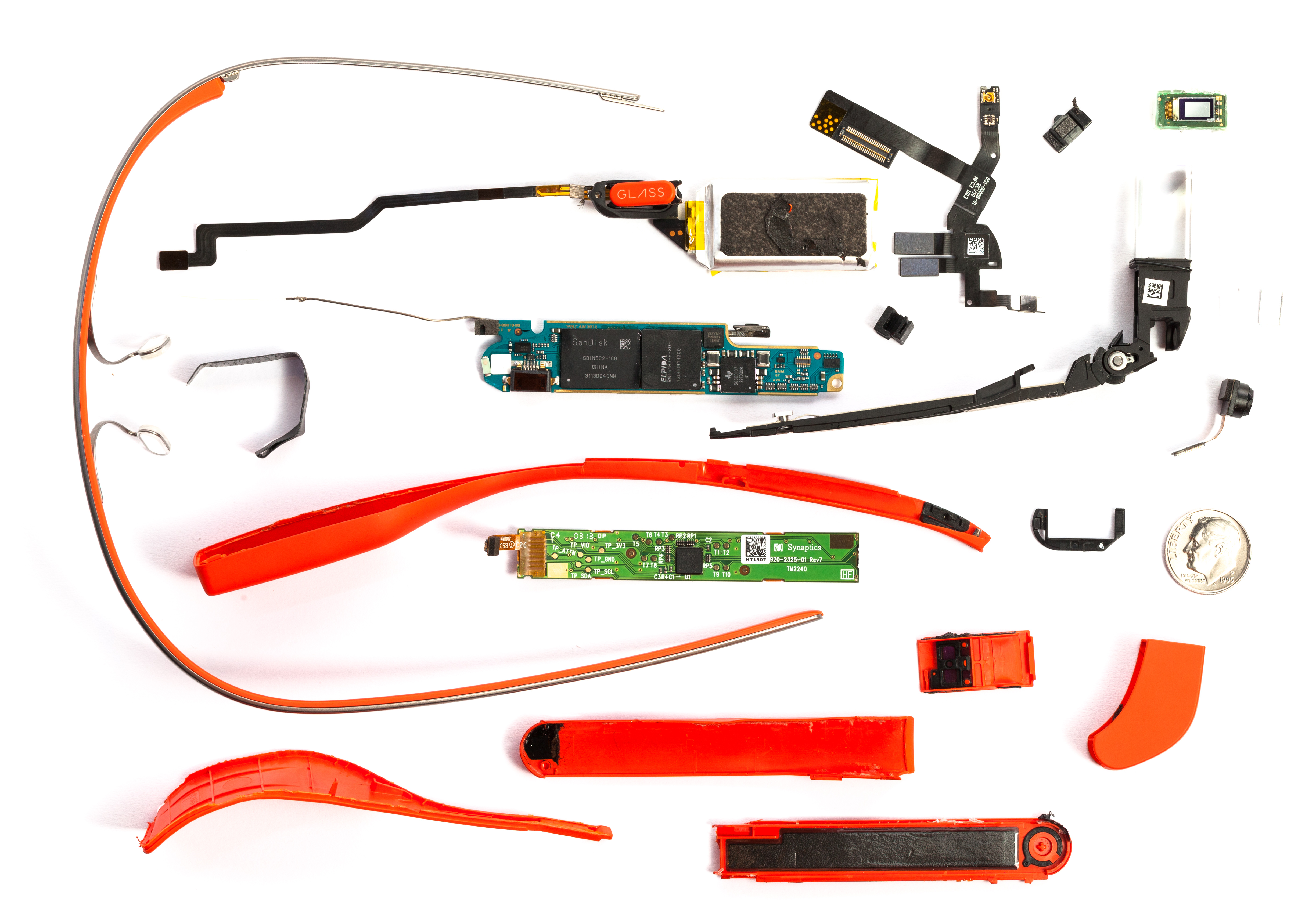
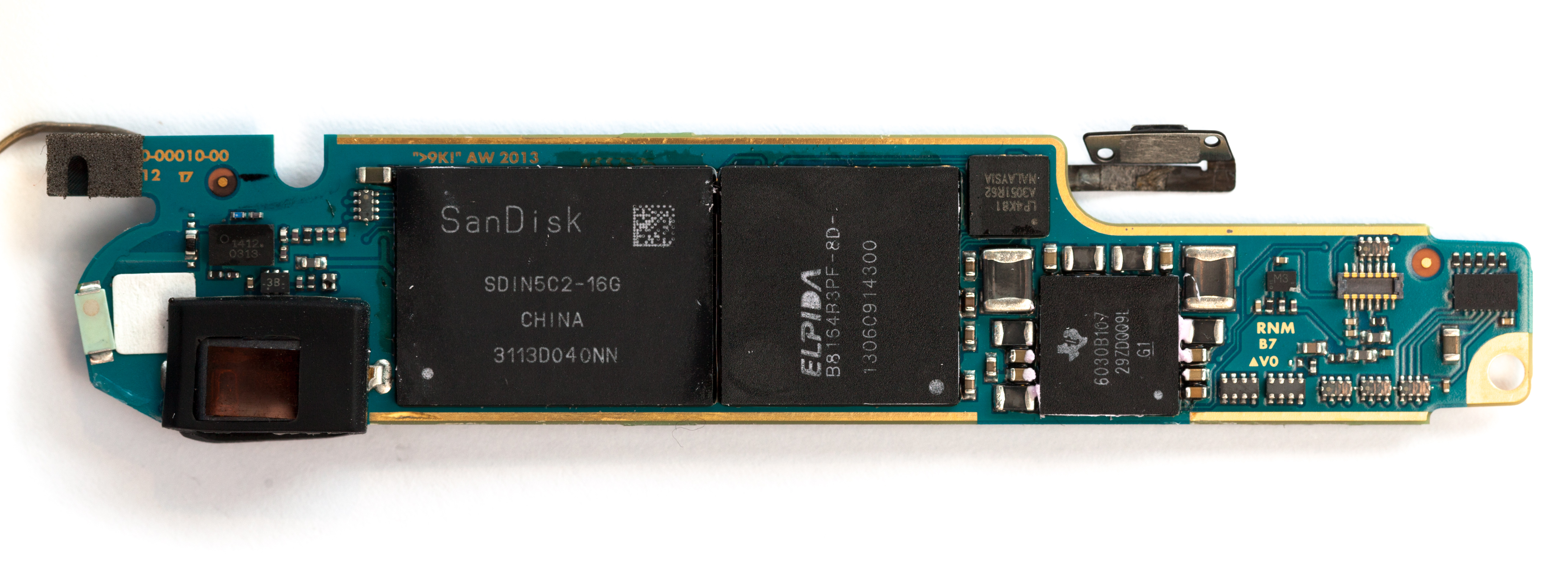
"core chips powering Glass: a TI OMAP4430, 16GB of SanDisk flash, and an Elpida mobile DRAM chip. "


Ron
Insightful, timely, and accurate semiconductor consulting.
Semiconductor information and news at - http://www.maltiel-consulting.com/

What is this Glass thing anyways?

Google's latest and hottest gadget needs little introduction.
Since its public unveiling in April 2012, the tiny head-mounted
Android computer has been collecting controversy and sociological
analysis. It is currently available in limited beta to eminent members
of the tech community and to a selection of "Glass Explorers". As
members of the latter program, we are delighted to be able to explore Glass.
.......

Side Touchpad

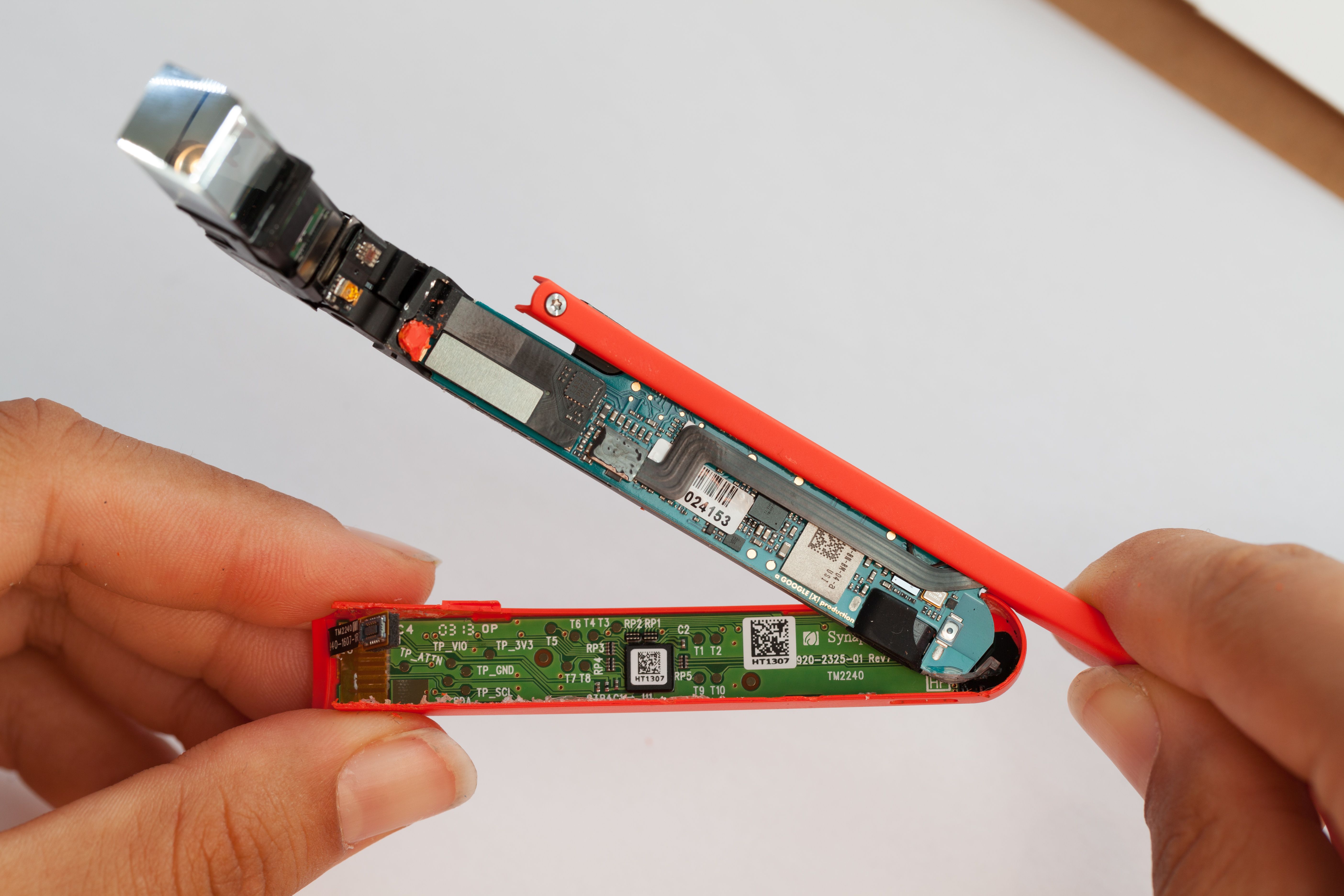
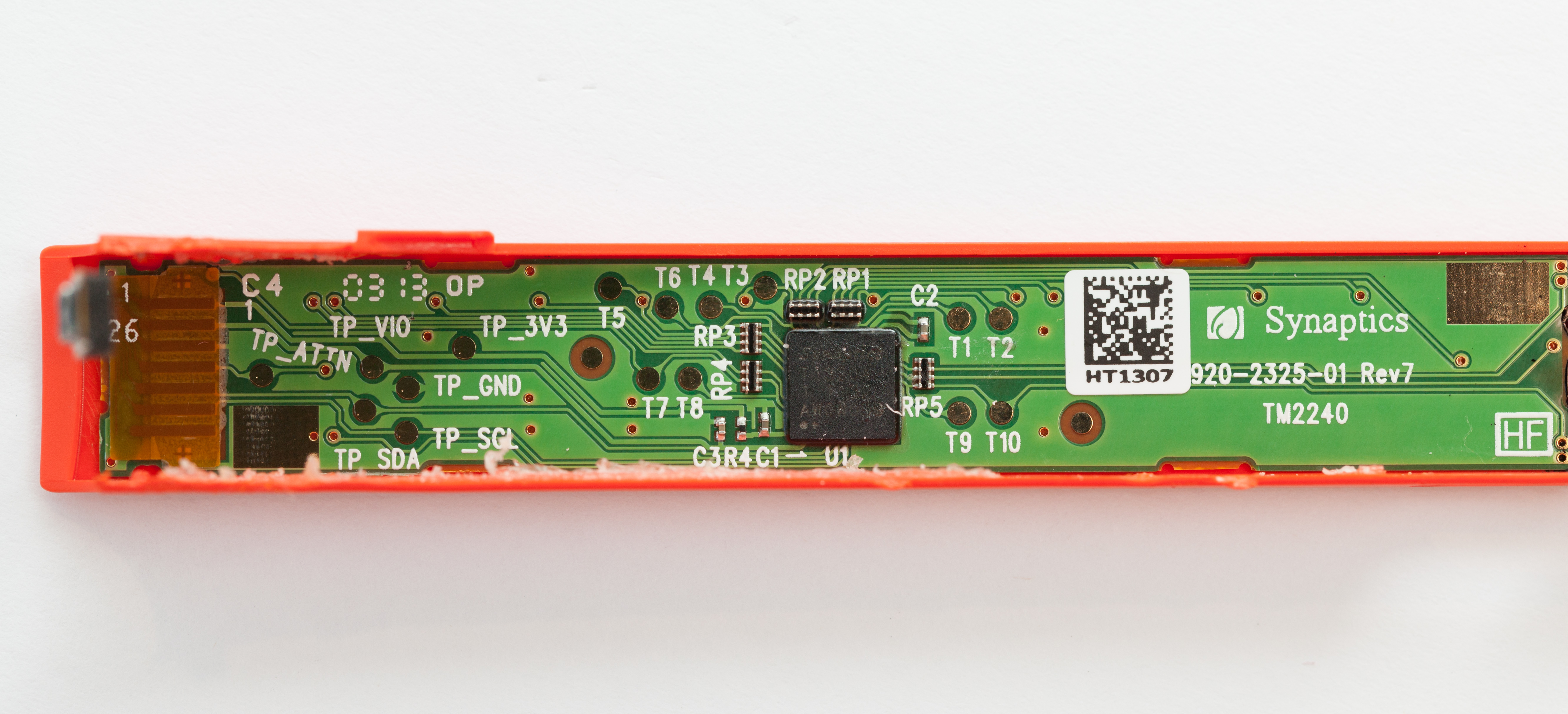
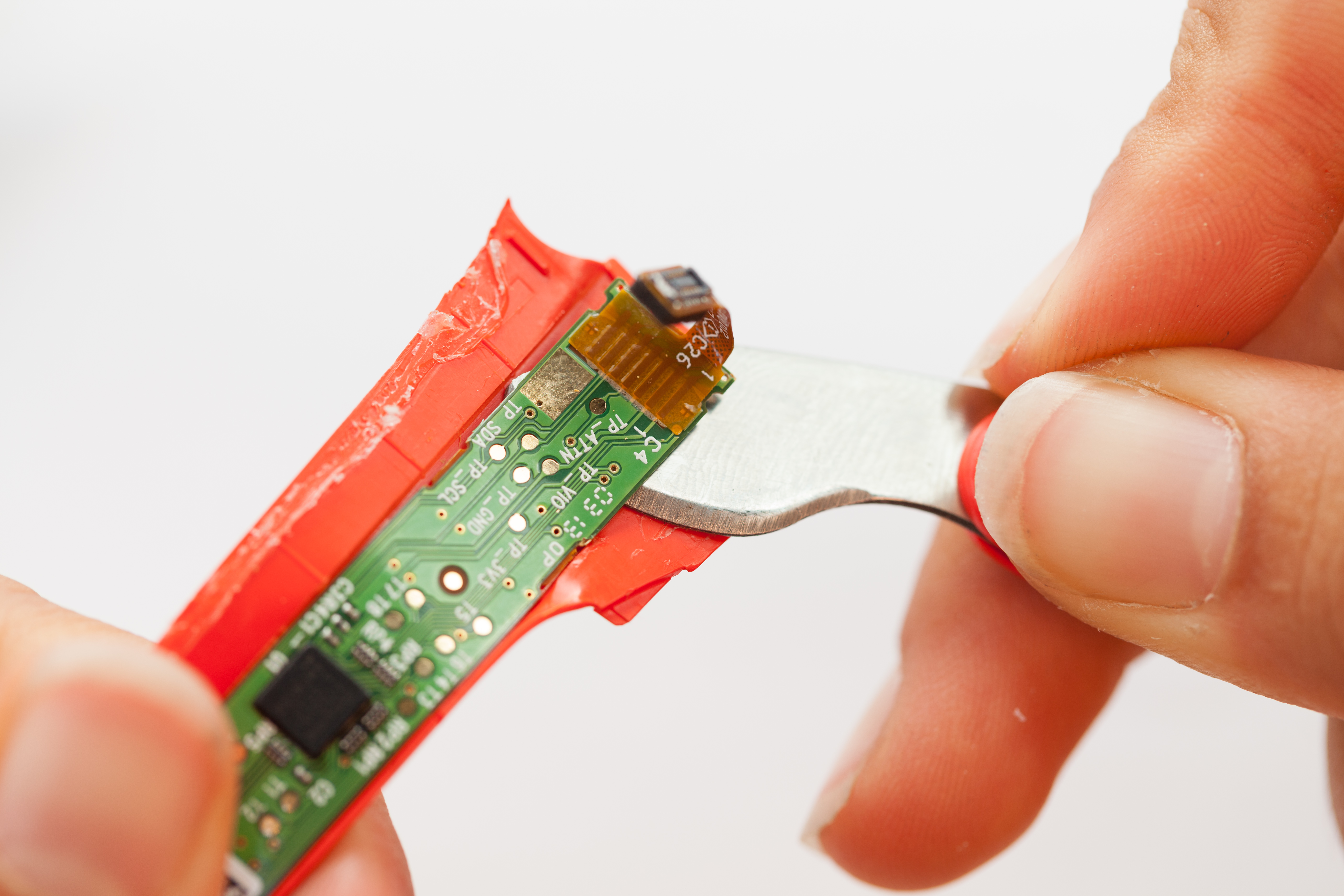
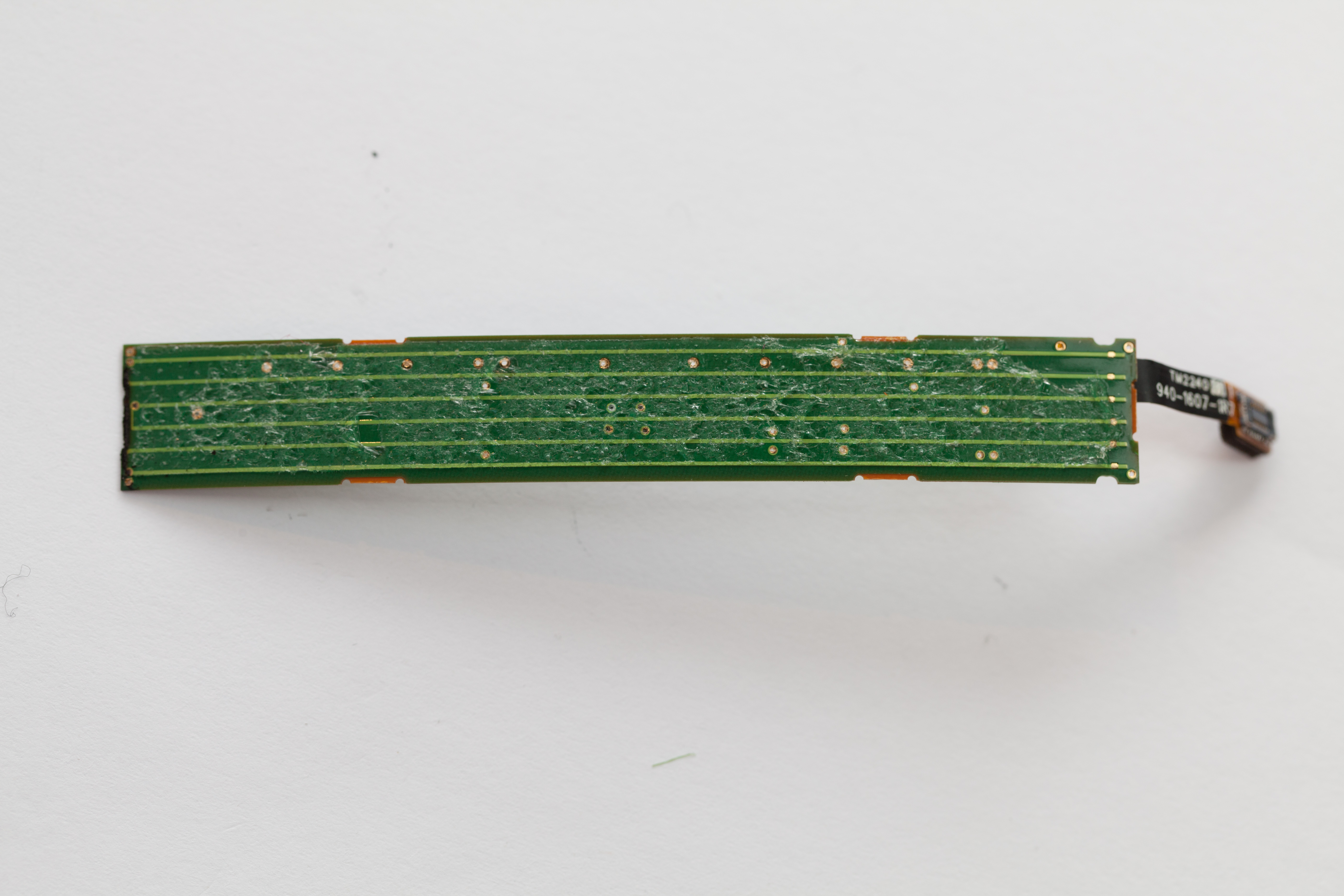
Removing the casing exposed a few parts, including the separate touchpad module on the right side of the unit. When a Glass users looks like they are pensively tapping their temple, they are interacting with this sensor. The touchpad is a full custom module made by Synaptics, and is driven by a Synaptics T1320A touchpad controller.

Main CPU Board

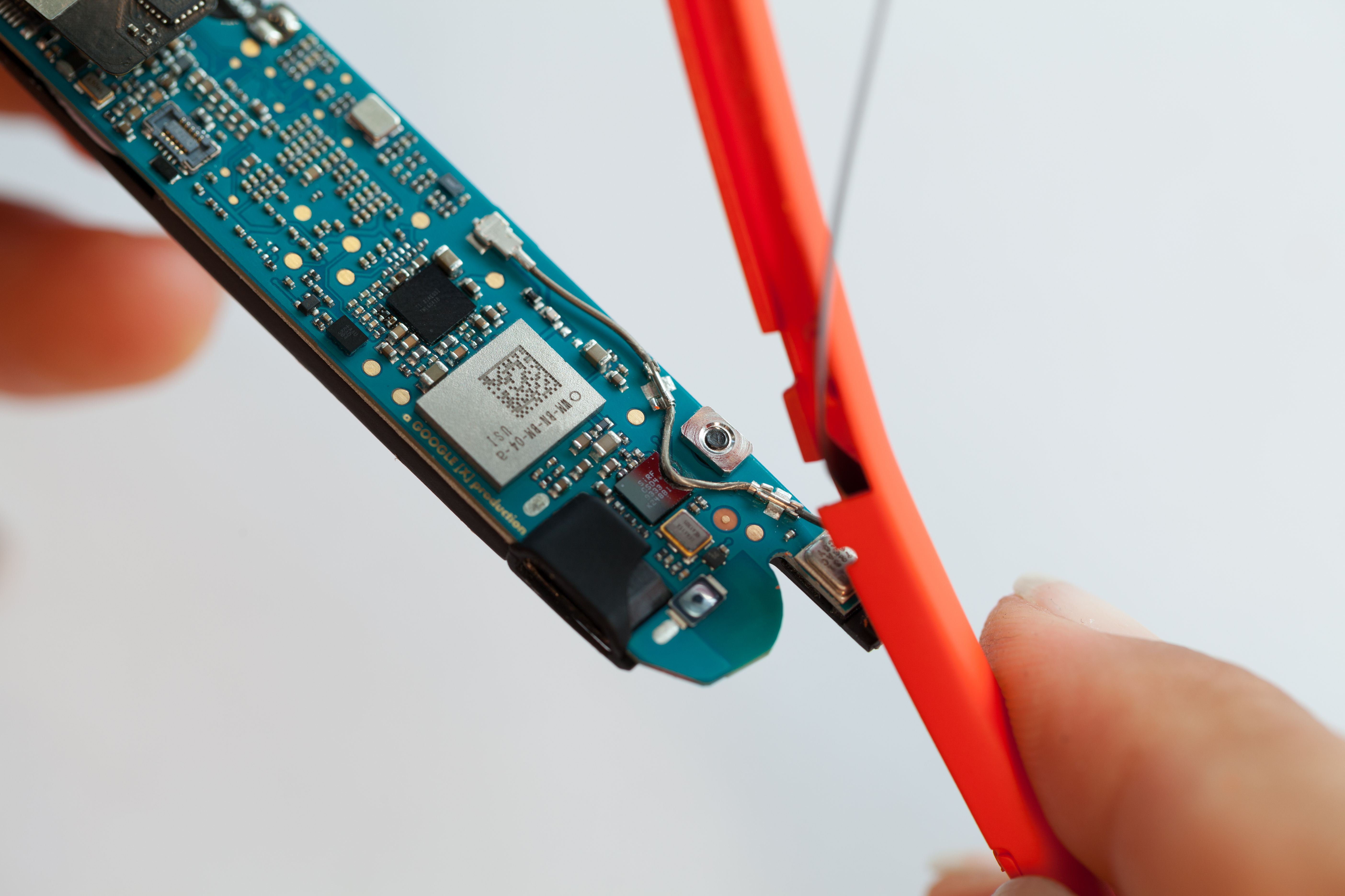
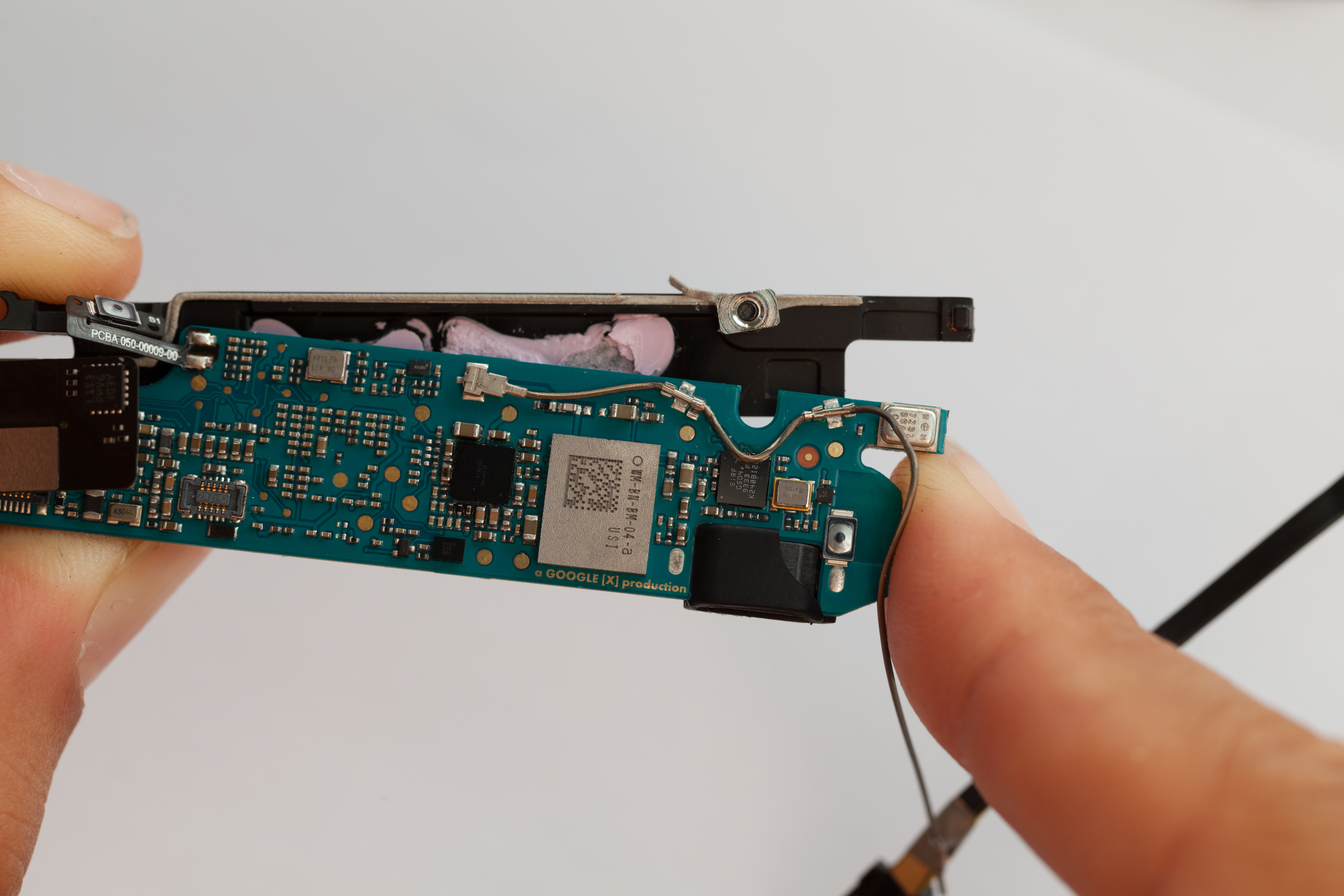
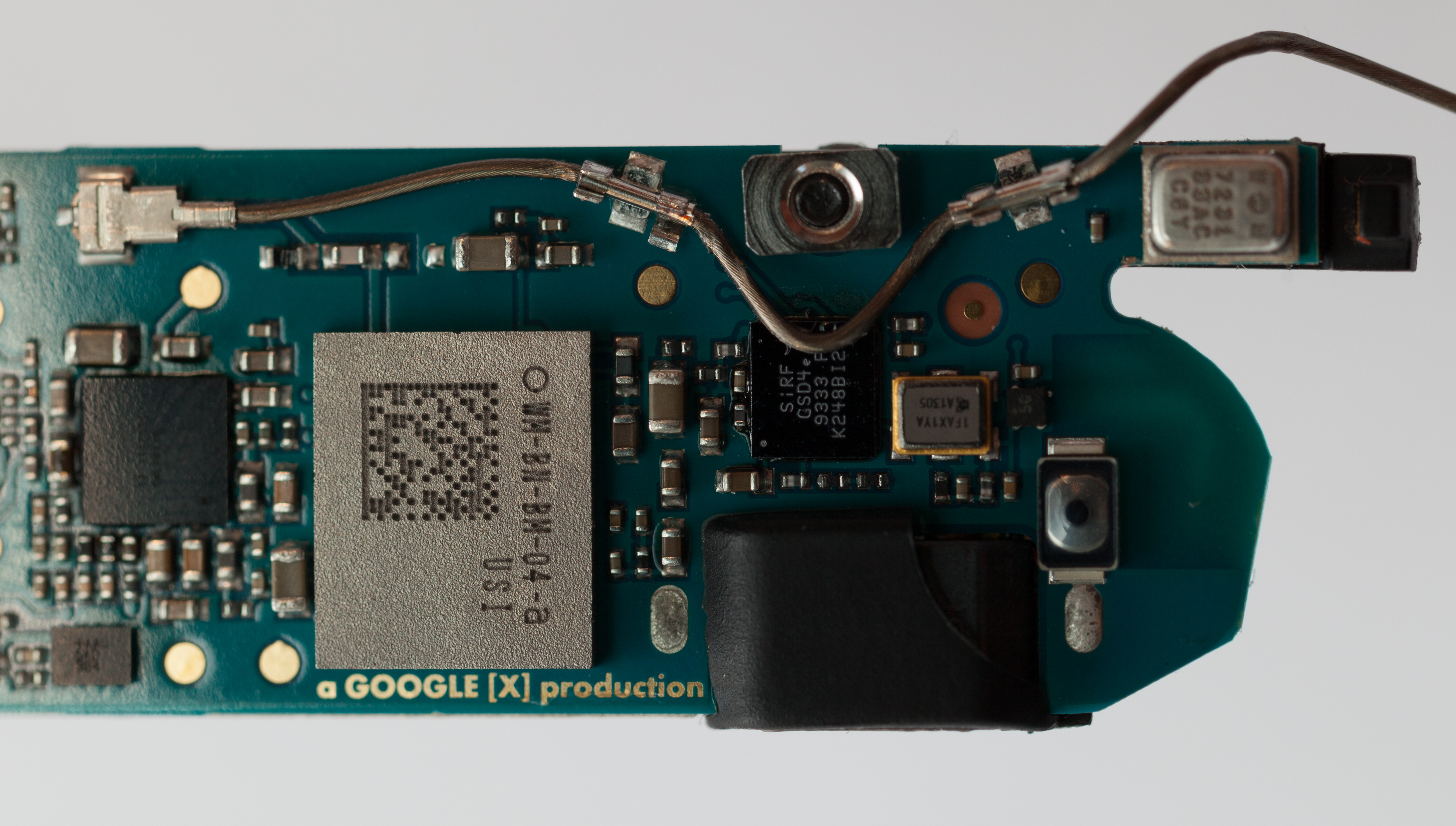
The main logic board was now exposed. The inwards-facing side holds an RF module, some small connectors and support ICs, and copper noting that this is "a GOOGLE [X] production".
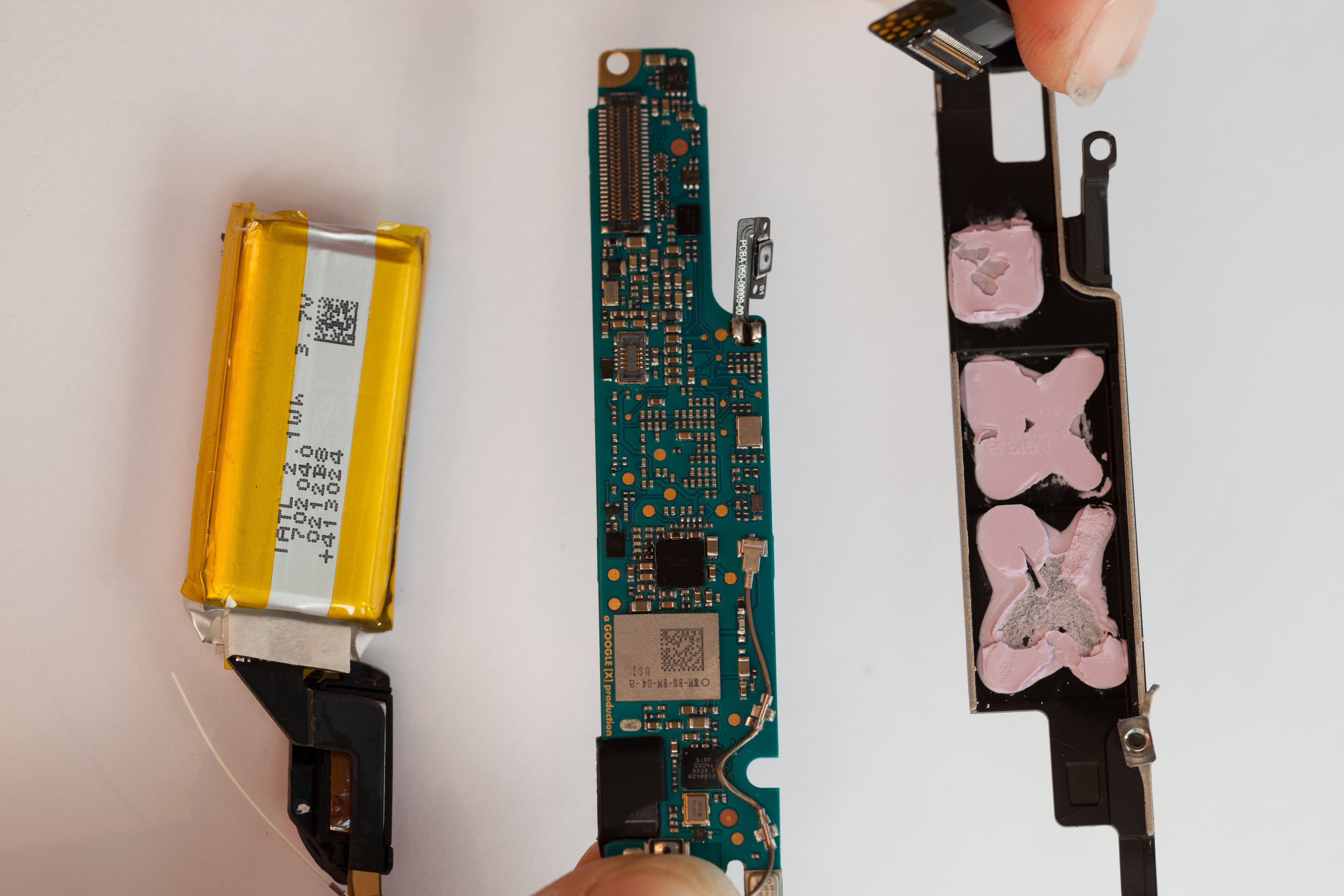
This board was stuck to a thermal pad with lots of paste. After removing it and cleaning off the pink thermal compound, we revealed the core chips powering Glass: a TI OMAP4430, 16GB of SanDisk flash, and an Elpida mobile DRAM chip. A flex PCB and an RF cable, anchored with some metal tabs and an MMCX (?) connector, trailed from this board to the behind-the-ear pod.
Some text in the copper on this board reads >9K!   It's over 9000!

Behind-Ear Module

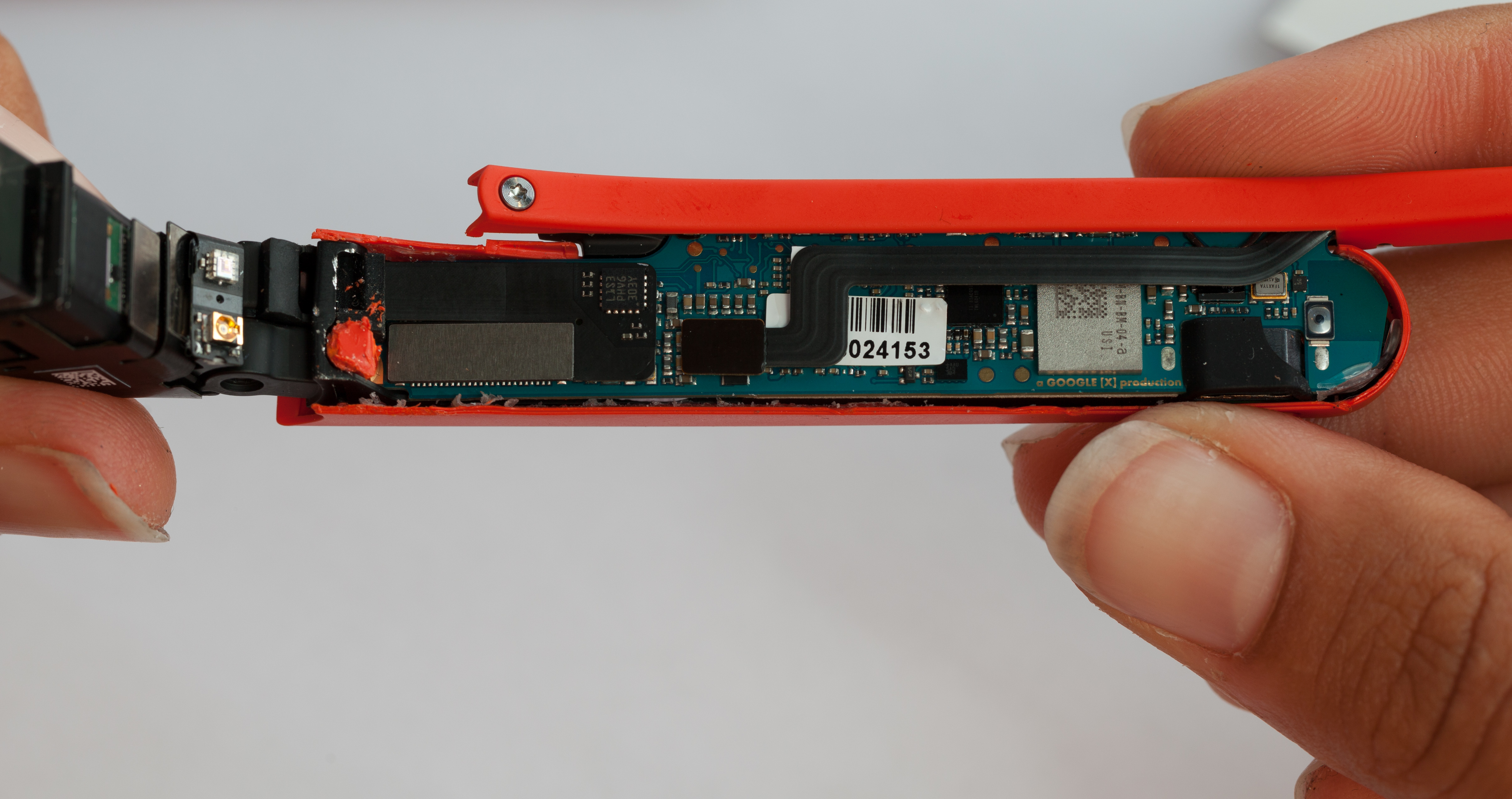
To keep the unit's weight distributed more evenly, Glass keeps its battery in a rounded bit behind the wearer's ear. We stripped this area open, again applying destructive force to tear the plastic.
The single-cell Lithium Polymer battery sits at the end of the flexprint PCB and is marked as having a capacity of 2.1 Wh (roughly 570 mAh). It is not user-replaceable, not even a little bit.