Showing posts with label NOR. Show all posts

Thursday, April 9, 2015

DRAM Market Consolidation=> 32% Growth, All Time High Revenue

6+ DRAM vendors in 2001
Worldwide semiconductor revenue grew 7.9% in 2014, led by DRAM 32% increases;

"memory market was the best performer for the second year in a row, growing 16.6 percent, meaning the rest of the market only achieved 4.9 percent growth," said Andrew Norwood, research vice president at Gartner. "As a group, DRAM vendors performed best, lifted by the booming DRAM market, which saw revenue increase 32 percent to $46.1 billion, surpassing the all-time high of $41.8 billion set in 1995." (more in the article below).  

The consolidation in the number of memory manufacturers from 20+ in the early 90s to 3 vendors help to firm DRAM memory chip price. Due to the limited number of vendors and the high cost of new fabs will keep the floor under DRAM chip costs in the future.


More about fab consolidation in my blog from March 2012 – Moore's Law End? (Next semiconductors gen. cost $10 billion)


Ron
Insightful, timely, and accurate semiconductor consulting.

Semiconductor information and news at - http://www.maltiel-consulting.com/


Worldwide Semiconductor Revenue Grew 7.9 Percent in 2014, According to Final Results by Gartner

Booming DRAM Market Sees Revenue Increase 32 Percent During 2014
Worldwide semiconductor revenue totaled $340.3 billion in 2014, a 7.9 percent increase from 2013 revenue of $315.4 billion, according to final results by Gartner, Inc. The top 25 semiconductor vendors' combined revenue increased 11.7 percent, which was more than the overall industry's growth. The top 25 vendors accounted for 72.4 percent of total market revenue, up from 69.9 percent in 2013.
"2014 saw all device categories post positive growth, unlike in 2013, when application-specific integrated circuits (ASIC), discretes and microcomponents all declined. The memory market was the best performer for the second year in a row, growing 16.6 percent, meaning the rest of the market only achieved 4.9 percent growth," said Andrew Norwood, research vice president at Gartner. "As a group, DRAM vendors performed best, lifted by the booming DRAM market, which saw revenue increase 32 percent to $46.1 billion, surpassing the all-time high of $41.8 billion set in 1995."
Intel saw a return to growth after two years of revenue decline, as PC production recovered, with sales up 7.7 percent (see Table 1). The company retained the No. 1 market share position for the 23rd consecutive year by capturing 15.4 percent of the market, which was down slightly on the previous year.
2014 saw significantly more merger and acquisition (M&A) activity among the major semiconductor vendors than the previous year, with some announced deals still to close in 2015. Among the most significant deals was Avago Technologies' acquisition of LSI, propelling the company into the top 25 semiconductor vendors for the first time. MStar Semiconductor was merged with MediaTek after a prolonged merger, and ON Semiconductor acquired Aptina Imaging. After adjusting for closed M&A activity, the top 25 semiconductor vendors grew at 9.1 percent.Source: Gartner (March 2015)
Additional information is provided in the Gartner report "Market Share Analysis: Semiconductors, Worldwide, 2014."

Monday, March 3, 2014

Flash NAND, NOR, eMMC Market Growth

NAND market continues to grow while NOR continue to shrink (see article below). 

The reason for NAND dominance were explained on my May 2007 article on Long Term Trends in the NOR and NAND Markets .


Highlights from review of the IHS report in the article below:
"NAND product known as embedded multimedia card (eMMC) enjoyed record shipments in 2013 of more than 1 billion units, up a hefty 49 percent from 687 million in 2012. NAND revenue rose 28 percent to US$25.8 billion.
In comparison, NOR shipments last year fell 10 percent to 606 million units, with revenue down 15 percent to approximately US$3.0 billion....
The evolution of eMMC, in particular, has been rapid, with nearly annual enhancements to performance. As an economical choice for greater flash-memory densities, eMMC has become viable in high-end markets like smartphones and tablets, in which high-density storage capacity is required along with low-power consumption and a small footprint.
Embedded NAND’s utility has also now carried over from smartphones in its early use, to tablets. Last year, eMMC was the standard memory configuration for a vast majority of tablets, the only exception being the Surface Pro from Microsoft, which employs a SATA-interface solid-state drive.
The billion-unit shipment level of eMMC last year is a milestone, Yang remarked, and the product shows the way forward for managed NAND solutions by its deft handling of error correction and enhanced reliability at the solution level."
Ron
Insightful, timely, and accurate semiconductor consulting.
Semiconductor information and news at - http://www.maltiel-consulting.com/


NAND eMMC hits a record year, while NOR Flash shrinks further

 
NAND eMMC hits a record year, while NOR Flash shrinks further
Source: IHS Technology, February 2014

The global memory market presented a vivid picture of contrast last year given the wildly divergent fortunes of its two main segments, with spritely NAND offset by the sobering continued downturn of beleaguered NOR flash, according to a new report from IHS Technology.
On the one hand, the NAND product known as embedded multimedia card (eMMC) enjoyed record shipments in 2013 of more than 1 billion units, up a hefty 49 percent from 687 million in 2012. NAND revenue rose 28 percent to US$25.8 billion.
In comparison, NOR shipments last year fell 10 percent to 606 million units, with revenue down 15 percent to approximately US$3.0 billion.
The overall flash market in 2013 was worth US$28.8 billion, up from US$23.7 billion a year earlier, as shown in the attached figure.
“The key driver to NAND lies in its proliferating use for mobile consumer electronics, exemplified by the memory’s increasingly widespread application in devices like smartphones, tablets and notebook PCs,” said Michael Yang, senior principal analyst for memory & storage at IHS.
“Meanwhile, NOR’s once-broad portfolio of applications in low-end mobile handsets and desktop PCs has mostly matured, and its next killer market has yet to manifest.”
These findings are contained in the report, “Mobile & Embedded Memory Tracker – Q4 2013,” from the Semiconductors & Components service of IHS.
NAND memory, in the form of either raw NAND or eMMC, is now the standard memory used for most smartphones. The only exception is Apple’s iPhone, which uses its own managed NAND memory product.
The evolution of eMMC, in particular, has been rapid, with nearly annual enhancements to performance. As an economical choice for greater flash-memory densities, eMMC has become viable in high-end markets like smartphones and tablets, in which high-density storage capacity is required along with low-power consumption and a small footprint.
Embedded NAND’s utility has also now carried over from smartphones in its early use, to tablets. Last year, eMMC was the standard memory configuration for a vast majority of tablets, the only exception being the Surface Pro from Microsoft, which employs a SATA-interface solid-state drive.
The billion-unit shipment level of eMMC last year is a milestone, Yang remarked, and the product shows the way forward for managed NAND solutions by its deft handling of error correction and enhanced reliability at the solution level.
The rise of eMMC has also bred a new cast of suppliers. While Samsung remains dominant, players like SK Hynix, SanDisk and Toshiba are fiercely competitive and poised to gain ground.
The eMMC space, however, could see challenges this year. With growth slowing in the smartphone and tablet markets, there could be a possible oversupply of the memory type, in the process also leading to a possible large drop in eMMC average selling prices.
The steady decline of the NOR flash market began in 2007 and hasn’t stopped since. At its peak, the NOR market exceeded US$9 billion a year and last hit US$8 billion back in 2006—a far cry from its current numbers.
The NOR picture is also complicated by the contrasting outlook for its two sub-segments.
Parallel NOR, long used in computers for boot-code execution or serving as a storage medium for entry-level cellphones, will see its run in wireless devices come to an end sometime next year.
Parallel NOR will continue to be used in high-level industrial, medical, networking and military applications, but its exit from wireless will be a blow.
Meanwhile, serial peripheral interface (SPI) NOR, rival to parallel NOR, will go on to wider use in both wireless and consumer devices.
SPI NOR’s relative simplicity in design and low manufacturing cost will prove appealing, and the memory will be especially attractive to manufacturers of low-cost cellphones that need to keep a lid on expenses.
The shift from parallel to SPI NOR has also impacted their respective suppliers. Micron Technology and Spansion, the foremost producers of parallel NOR, now also have SPI offerings.
However, both companies have been at pains to differentiate their SPI product from the rest of the pack, in order to stave off the aggressive penetration of other SPI NOR suppliers such as Macronix, Winbond Electronics and GigaDevice.
The ongoing growth of SPI NOR will help offset a shrinking parallel NOR market, but the industry would be healthier if consolidation took place and reduced the number of players to four, IHS believes.
There are five suppliers at present that command 75 percent of the market, along with a spattering of smaller producers that make up the rest of the market.
Even so, there are no quick fixes, with the largest NOR applications disappearing or on their way out, and new deployments like automotive NOR still facing an uphill climb.

Friday, March 22, 2013

Tablets are the New Mobile


Tablets are the new mobile, the slide deck in the article shows the growth of mobile, tablets in the Apple and Android eco-sphere. there are many other slide at the link below. The future of mobile follows the trajectory of April 15, 2009 Mobile Computing the Next Big Market.

Ron

Insightful, timely, and accurate semiconductor consulting.Semiconductor information and news at - www.maltiel-consulting.com

Future Of Mobile [SLIDE DECK]


Henry Blodget and Alex Cocotas | Mar. 21, 2013, 11:37 AM

Read more: http://www.businessinsider.com/the-future-of-mobile-slide-deck-2013-3?op=1#ixzz2OHIaEnKc

To kick off the conference, our BI Intelligence team—Marcelo BallvĂ©, Alex Cocotas, and I—put together a deck on the current trends in mobile. We looked closely at the growth of smartphone and tablet adoption, the platform wars, and how consumers are actually using their devices.
See more 


Thursday, January 3, 2013

Flash Memory Growth & Sales Surpass DRAM


See in August 2012 Flash Memory Sales Surpass DRAM  , and DRAM Market Plateau/ Flash NAND Growing

While the NOR market size is not growing as fast as NAND market it is still big enough to make the combined flash market bigger than DRAM market.

More on NOR market in a previous comments Flash NOR Memory Revival and in my May 2007 article on Long Term Trends in the NOR and NAND Markets

Ron


http://www.maltiel-consulting.com/


Flash overtakes DRAM
David Manners,   Thursday 20 December 2012 10:09

The flash memory market will grow 2% to $30bn in 2012, overtaking the $28bn DRAM market for the first time, says IC Insights.

With the exception of 2010, the DRAM and flash memory markets have been growing closer in size to each other for several years but demand for flash used in portable media devices, coupled with two years of weaker demand and price erosion for commodity DRAM used in personal computers, will finally be enough to push total flash sales beyond those for DRAM this year, says IC Insights.

Among portable media devices, smartphone shipments are projected to finish the year up 55% to 750 million units and shipments of tablet computers are forecast to rise 80% to 117 million units.

Through 2017, the flash memory market is expected to widen its lead over DRAM. In fact, IC Insights forecasts the NAND flash memory market alone will be larger than the DRAM market beginning in 2013.

Among more than 30 product segments classified by WSTS, NAND flash is forecast to have the third-highest average annual growth rate through 2017, trailing only the market growth rates for tablet processors and cellphone application processors.
NAND flash sales are forecast to increase 14% annually from 2012-2017, growing to $53bn at the end of the forecast period while the DRAM market is forecast to grow 9% annually over this same time.

Thursday, October 25, 2012

Mobile DRAM Takes Over

"mobile DRAM commanded more than 26 percent of all DRAM revenue during the second quarter—a significant improvement from 19 percent the same time a year ago, and from 11 percent two years ago in 2010.
This is attributed to 2 reasons:
1. Share of mobile DRAM bit shipments is now at 17.8 percent, up from 7.9 percent in the first quarter.
2. The price of mobile DRAM has fallen less than that of its commodity cousin and its pricing is overall less vulnerable given the segments it plays in."(from Mobile DRAM Market Grows, Samsung Domination Continues)

Ron
www.maltiel-consulting.com


Mobile DRAM revenues up in 2nd Quarter

Thursday, October 18, 2012


Mobile DRAM revenues rose to the highest level yet in the second quarter of 2012 Revenues amounted to US$1.85 billion in the second quarter, up from US$1.83 billion in the first.

Two reasons account for mobile DRAM's rising market clout. First, mobile DRAM's share of total DRAM bit shipments is now at 17.8%, up from 7.9% in the first quarter.

Second, the price of mobile DRAM has fallen less than that of itsd cousin, commodity DRAM, IHS noted. While commodity DRAM historically has been subject to great swings in pricing—with the product losing as much as half of its value from the second to the fourth quarter last year alone—mobile DRAM pricing is less vulnerable, falling 10% per quarter on average.

Mobile DRAM also tends to be priced according to manufacturing cost, not based on the general balance between supply and demand. As a result, DRAM companies are able to earn a more reasonable margin for their mobile memory products—unlike in commodity DRAM, where negative margins are frequently the rule.

Samsung Electronics continued its unshakable hold at the top of the mobile DRAM market in the second quarter of 2012, with sales of US$1.1 billion, or a remarkable 61% of the global mobile DRAM market.

With the success of smartphones such as the Galaxy S3, the South Korean electronics titan also is now one of the world's largest consumers of mobile DRAM. Samsung enjoyed a 3% improvement in sales during the quarter, and its year-to-year growth was even more impressive at 35%.

SK Hynix was No. 2 behind Samsung with sales of US$362 million, down from US$366 million in the first quarter and from US$377 million the same time a year ago.

Elpida Memory snagged a 13% share based on mobile DRAM revenues of US$245 million in the second quarter of 2012, while Micron Technology saw its share amount to 4% in light of US$79 million in revenues.
By: DocMemory

Tuesday, October 2, 2012

DRAM Market Plateau/ Flash NAND Growing

While the PC market is slowing as the article below discusses, the Tablet and iPad are new markets that should offer growth opportunities for both Flash NAND and DRAM.

The key reason that DRAM is slowing while NAND (and NOR) are growing faster is due to the inherent advantages of Flash vs. DRAM.


We can already see that Flash Memory Sales Surpass DRAM  additional reasons were mentioned in the March 2012 article When will Flash Memory Market be 2x of DRAMs


Ron
http://www.maltiel-consulting.com/


DRAM Makers Continue to Suffer as DRAM Price Falls

http://www.xbitlabs.com/news/memory/display/20121032152632_DRAM_Makers_Continue_to_Suffer_as_DRAM_Price_Falls.html
4GB DDR3 DRAM Module's Price Drops to $16.25

by Anton Shilov 10/01/2012 

Dynamic random access memory (DRAM) market monitoring company DRAMeXchange claims that as notebook shipments show signs of weakening and Windows 8 looks unlikely to stimulate PC shipments, second-half September contract price continues on a downtrend.

Average transaction price per 4GB DDR module fell from $17.25 to 16.25, with a low of $16, close to the lowest price reached during the second half of 2011. Average 2GB module price, on the other hand, has dropped to $9.25, a 5.13% decrease compared to the first half of the month. As 4GB modules have replaced 2GB modules as the market mainstream, 4GB price drops have become more apparent.

At press time, one untested [eTT] 2Gb DDR3 chip price cost $0.683 on average in Taiwan's spot market, 2Gb DDR3 1333MHz/1600MHz chip's price was approximately $0.844, whereas 4Gb DDR3 1600MHz memory IC was priced at $2.545 on average on the spot market.

From the market perspective, DRAM average selling price has been plummeting at an increasing rate since July, reflecting not only weaker-than-expected seasonal demand, but also the fact that supply-side adjustments were not as effective as hoped. Using 4GB module price as the basis of calculation, 2Gb chip price has plunged to a low of $0.84, arriving at spot price levels. Looking at the spot market, as purchasing is weak, module makers are less eager to restock inventory. Both contract and spot prices reflect price negotiation difficulties, and transaction volume has been much lower than last quarter, clear indication that both module makers and PC OEMs have high stock levels; thus, buying momentum is not likely to pick up in the short term. In the absence of large-scale production cuts, TrendForce expects contract price will remain on a downtrend.

As the PC market has matured in recent years, in addition to the fact that the global economy is expected to worsen in the second half of this year, TrendForce forecasts PC shipments will see -3.9% growth for 2012. Furthermore, as consumers’ limited budgets and changing preferences steer them towards other mobile devices, smartphones and tablets are experiencing high growth while the PC market suffers. It is clear that PC demand is not as it was; the category is no longer the market mainstream, as shown by the fact that the 2012 PC DRAM shipment ratio has fallen below 50% for the first time.

On side, although makers are beginning to favor non-commodity DRAM production, PC DRAM supply is still in excess, which indicates restoring the supply-demand balance can no longer be achieved via production adjustments. A portion of commodity DRAM capacity must be permanently reduced if industry supply levels are to be lowered. According to TrendForce data, 2HSept. 4GB module price is approaching last year’s low, and is already below every DRAM maker’s total cost (based on mainstream 30nm process). Losses from commodity DRAM are not decreasing, and price is expected to continue falling in the short term unless large-scale capacity cuts are initiated.

Monday, September 24, 2012

NAND:Prices, Market Shares (Micron Up, Toshiba Down..)


NAND flash market share in July 2011
 Micron was able to increase its market share in NAND flash to 20.7%. based on IHS's report:

"Micron was able to claim some of the market share ceded by Toshiba. The Japanese maker in the second quarter saw its share decline by 9.5 percentage points sequentially, which occurred after strong growth in the first quarter....
Micron accounted for 80 percent of production from its joint venture with Intel, up from 62 percent in the first quarter. The increase was part of a revised capacity agreement between the two companies."


The pie chart shows how much Micron's market share improved since July 2011. (via https://www.semiconportal.com/en/archive/news/main-news/110715-toshiba-fab5-nand.html).


Since July 2011, NAND prices have been trending down. From the second article below:

"over the last two or so years, Micron, Samsung, SK Hynix and Toshiba began to expand their NAND production at a dramatic pace. The goal was to meet the anticipated demand for the next wave of product drivers, such as smartphones, solid-state drives (SSDs), tablets and ultrabooks.
Seeking to drive down product costs, particularly for SSDs, NAND vendors took the lead in process technology. For example, the Toshiba-SanDisk duo has been ramping up parts based on the world’s most advanced process, a 19nm technology.
The bottom fell out of the NAND market in recent times. NAND vendors built up too much fab capacity. Average selling prices (ASPs) for NAND fell by 46% in the first half of 2012. Demand for NAND in smartphones and tablets remains overwhelming, but SSD and ultrabook shipments have been disappointing thus far."


Ron
http://www.maltiel-consulting.com/


In a First, U.S.-Based Micron Takes 20 Percent Share of the NAND Flash Market

http://www.isuppli.com/Memory-and-Storage/News/Pages/In-a-First-US-Based-Micron-Takes-20-Percent-Share-of-the-NAND-Flash-Market.aspx
Dee Nguyen,     September 21, 2012

For the first time since it entered the industry seven years ago, U.S.-based Micron Technology Inc. managed to cross the 20 percent market share threshold in the NAND flash memory business during the second quarter.

Micron posted the strongest sequential performance of all NAND suppliers, with second-quarter revenue amounting to $897 million, up 6 percent from $846 million in the first quarter, according to an IHS iSuppli
In comparison, the other ranked suppliers all suffered revenue declines during the same period.

Despite overall NAND flash market revenue declining by 13 percent, Boise, Idaho-based Micron increased its market share to 20.7 percent in the second quarter, up from 17 percent in the first quarter, as presented in the table below.


“Defying weak demand and falling prices in the overall business, Micron expanded its NAND revenue and market share to reach the key 20 percent milestone for the first time since it started selling the memory in 2005,” said Dee Nguyen, memory analyst at IHS. “Micron not only successfully increased its bit shipments of NAND flash by a whopping 68 percent, it also benefitted from a reallocation in production from the NAND joint venture partner with Intel Corp., while capitalizing on the travails at its close competitor—No. 2-ranked Toshiba Corp.”

Intel and Toshiba Benefit Micron

See the rest at www.maltiel-consulting.com/nandprices-market-shares-micron-up.html


NAND Enters Tough Cycle

http://semimd.com/blog/2012/09/20/nand-enters-tough-cycle/
By Mark LaPedus

The NAND flash memory market is entering into a new and painful cycle, a period that will impact suppliers, OEMs and fab tool vendors alike.

For some time, there has been an oversupply and depressed pricing in the NAND market. In mid-2011, Micron, Samsung, SK Hynix and Toshiba put on the brakes in their capital spending plans. And in recent months, NAND suppliers in total have announced plans to cut 150,000 wafer starts per month, or about 12% of the world’s NAND capacity, amid ongoing losses and sluggish demand.

Just as suppliers moved to cut their production, spot shortages of NAND surfaced at some OEMs in early September. Most OEMs are not seeing any shortages, but that could all change. Apple, the world’s largest buyer of NAND, could cause some gyrations in the channels as it ramps up its new iPhone 5.

So what’s the outlook in the fluid and confusing NAND market? Amid a bitter legal battle with Samsung, speculation is rampant throughout the NAND industry about whether Apple will swap suppliers from Samsung to SK Hynix, Toshiba and Micron. If that happens, Samsung would face an oversupply in NAND, while others may see capacity shortfalls.

The outlook is also not so rosy for fab tool vendors, which counted on a big capital spending cycle for NAND. In fact, NAND suppliers are expected to push out their capital spending plans until June of 2013 and perhaps beyond, said Vijay Rakesh, an analyst with Sterne Agee.

The lack of capital spending is expected to create a shortfall in NAND capacity, creating perhaps a long cycle of acute shortages. Presently, there is a capacity glut for NAND. “Demand should catch up with capacity by mid-2013,” said Jim Handy, an analyst with Objective-Analysis. “Then, there could be NAND shortages from then until the middle of 2015.”

See the rest at www.maltiel-consulting.com/nandprices-market-shares-micron-up.html

Friday, September 7, 2012

iPad, iPhone and Tablets=> Flash, DRAM Markets Crosscurrents

The article below discuss shifting crosscurrents in the flash and DRAM markets. iPad, iPhone and Tablets impact Flash, DRAM chip markets. Expected demand for iPhone, iPad, Amazon fire and other tablets drive up expectation for chip markets.

Some of the key crosscurrents
"Many of the leading NAND flash suppliers, including Toshiba, Samsung and Micron have significant commitments to Apple Inc. to supply NAND flash. Apple is reported to have recently cut its order of NAND flash memory from Samsung. It is not clear whether OCZ's "industry-wide" supply shortage could have resulted from NAND flash memory inventory being taken up for use by Apple in its forthcoming model of iPhone expected to launch on Sept. 12."


Impact of legal patent figths of Apple and Samsung are discussed in the next blog.

Ron Maltiel


NAND flash memory in short supply

http://www.eetimes.com/electronics-news/4395618/NAND-flash-in-short-supply-after-production-cuts
Peter Clarke  9/7/2012 6:22 AM EDT


LONDON – Just six weeks after Toshiba Corp. announced it was cutting its production of NAND flash chips by about 30 percent due to market oversupply and chip price concerns, a maker of solid-state drives has signaled it can't get enough of the memory chips.

"Despite achieving bookings in excess of our expectations for our second fiscal quarter, we were not able to meet our previously stated revenue guidance due primarily to constraints in NAND flash supply," said Ryan Petersen, CEO of OCZ Technology Group Inc. (San Jose, Calif.), in a statement on the company's second fiscal quarter financial results, issued Wednesday (Sept. 5). "During the month of August we experienced a significant shortage on certain NAND flash components, based on industry-wide tightening of supply, leaving OCZ with an undersupply of the 2X-nm MLC NAND used in our Vertex and Agility Line of products," Petersen said.

"While we believe that the situation will resolve itself, subject to market conditions, we plan to hasten our transition to new process nodes in order to help ease these supply constraints," added Petersen.
When Toshiba announced the immediate cut in production in July it said it expected the supply and demand balance to improve in the third quarter due to growth of PC and smartphone shipments and that it would continue to monitor the situation and resume production ahead of increasing demand.

Many of the leading NAND flash suppliers, including Toshiba, Samsung and Micron have significant commitments to Apple Inc. to supply NAND flash. Apple is reported to have recently cut its order of NAND flash memory from Samsung. It is not clear whether OCZ's "industry-wide" supply shortage could have resulted from NAND flash memory inventory being taken up for use by Apple in its forthcoming model of iPhone expected to launch on Sept. 12.

Wednesday, August 22, 2012

Flash Memory Sales Surpass DRAM

Combined NOR and NAND flash Flash memory together already surpassed DRAM sales. See from the article below NAND and DRAM market size -

"the size of the markets is now relatively similar (about $26 billion to $28 billion for NAND, and about $28 billion to $30 billion for DRAM)"

While the NOR market size is not growing as fast as NAND market it is still big enough to make the combined flash market bigger than DRAM market.

More on NOR market in a previous comments Flash NOR Memory Revival and in my May 2007 article on Long Term Trends in the NOR and NAND Markets


Ron
http://www.maltiel.com/flash-news.html


When will NAND sales surpass DRAM?

Dylan McGrath , 8/16/2012 9:08 PM EDT

Mobility—smartphones and media tablets—is the driving force in electronics today. PC sales, meanwhile, are sluggish, with a forecast growth rate of only about 5 percent, according to International Data Corp.
Despite that, sales of DRAM—the main memory in PCs—remain greater that those of NAND, and are likely to stay that way for at least the next couple of years, according to market researchers. IC Insights, which expects total flash memory sales to eclipse DRAM sales for the first time this year, expects NAND to overtake DRAM sales in 2014. IHS iSuppli, however, forecasts that DRAM will remain in the lead through at least 2016.

Mike Splinter, chairman and CEO of chip equipment vendor Applied Materials Inc., was asked during a conference call following Applied's quarterly report Wednesday (Aug. 15) when he expected the NAND market to overtake the DRAM market.

"I think that's really totally dependent on solid-state drives," Splinter said. He had noted earlier in the call that adoption of SSDs is not happening as quickly as forecast.
"We've been quite disappointed that tablets and smartphones haven't accelerated the use of flash capacity," Splinter said. He added that Applied's hope now is that SSDs will take off with the introduction of ultrabooks—the thin, low power notebook PC concept being driven by Intel Corp.

Splinter noted that the size of the markets is now relatively the similar (about $26 billion to $28 billion for NAND, and about $28 billion to $30 billion for DRAM). Despite analysts' forecasts, Splinter suggested that a surge of NAND buying could cause it to overtake DRAM as quickly as next year.
Is such a surge in the cards? According to Splinter, that's up to SSDs.

Monday, July 16, 2012

Flash NOR Memory Revival

NOR flash memory is being replaced by NAND in smart phones.  NOR, however, is finding new growth opportunities in tablets, automotive, and industrial computers as the article below discusses.  These new markets will help strengthen NOR's market share but it will not become as big as the NAND market.

Additional info is in my May 2007 article on Long Term Trends in the NOR and NAND Markets .


Ron


NOR Flash Makers Find New Growth Areas to Compensate for Slowing Sales in Cellphones, Teardown Results Reveal


July 13, 2012
http://www.isuppli.com/Memory-and-Storage/News/Pages/NOR-Flash-Makers-Find-New-Growth-Areas-to-Compensate-for-Slowing-Sales-in-Cellphones-Teardown-Results-Reveal.aspx
Ryan Chien


NOR flash memory sales growth may be tapering off in mobile handsets and smartphones, but lucrative embedded applications in the tablet, automotive and industrial markets are picking up the slack, according to the IHS iSuppli Storage Service at information and analytics provider IHS (NYSE: IHS).


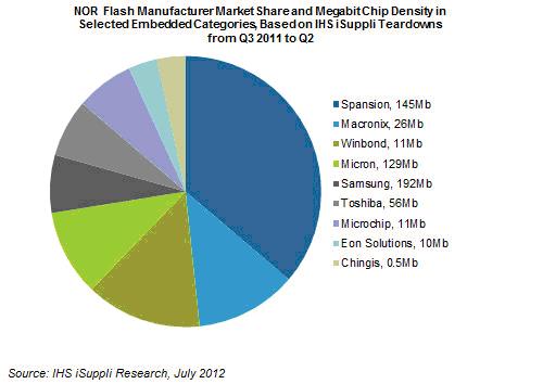
Based on a sample of 55 embedded products dissected by the IHS iSuppli Teardown Analysis Services over the course of three quarters, California-based Spansion Inc. led all NOR suppliers in terms of design wins. The company accounted for more than one-third of the NOR chips in the torn-down devices, as shown in the figure below.


Spansion, together with Samsung Electronics Co. Ltd. of South Korea and Micron Technology Inc. from Idaho, offered NOR chips in densities averaging in the hundreds of megabits. The three companies accounted for 53.4 percent of NOR chips in the three subsegments during the period from the third quarter of 2011 to the second quarter this year.


The rest of the market, equivalent to 46.6 percent of the sample, is controlled by companies that produced low-density NOR memory below the 100-megabit level. This group included big players like Taiwan’s Macronix International Co. Ltd. and Winbond Electronics Corp., as well as smaller entities like fellow Taiwanese firms Chingis Technology Corp. and Eon Silicon Solution Inc.


“Used to store small amounts of executable code, NOR flash was traditionally employed in devices like cellphones for fast read operations and random access capabilities,” said Ryan Chien, analyst for memory and storage at IHS. “However, newer implementations of NAND-based Embedded MultiMedia Card (eMMC) solutions that emulate NOR capabilities have resulted in NOR falling out of favor. The percentage of handsets using NOR flash has fallen from 14 percent in 2010 teardowns to less than 7 percent since then, found mostly in Samsung smartphones. However, NOR manufacturers have been proactive in their diversification efforts, borne out by a study of recent teardowns in both wireless and embedded categories.”


Tablets Energize NOR Market

Among the most prominent applications for NOR are tablets. Despite the elimination of NOR in the new iPad from Apple Inc., NOR chips were found in several Android alternatives in the teardowns, including the Eee Slate and Transformer Prime from Asus; the Jetstream and Flyer from HTC; and the Galaxy Tab 10.1 LTE and 7.7 from Samsung. Tablet devices from Samsung tended to incorporate the company’s own brand, higher-density NOR flash in multi-chip packages, while other branded tablets preferred discrete low-density SPI parts.


In the automotive space, NOR flash plays an increasing role to address vehicle safety regulations and manage user-comfort expectations. Head units in vehicles from Ford, General Motors, Nissan and Honda each had more than 230 megabits of NOR flash. NOR suppliers include Microchip and Micron for Honda and Toyota cars; Toshiba Corp. for Nissan vehicles; and Spansion for GM and Ford autos.


The other high-potential market for NOR flash is the industrial space. Network-attached storage systems from QNAP Systems and Buffalo Technology use Micron chips, and routers from Ubee Interactive and Ruckus Wireless each include 128 megabits of NOR.


An emerging industrial segment for NOR is the smart grid space, where devices such as feeder protection relays require high-density NOR to help monitor substation power lines. All of the NOR flash in hardware made by Sweden’s ABB Group is from Spansion, while solutions for U.S.-based Schweitzer Engineering Laboratories make use of Samsung and Spansion NOR parts. Samsung NOR is rare in third-party products, whereas Spansion has been aggressive in addressing this growth segment.


Friday, June 8, 2012

Cloud Storage, Servers Drive IC Demand

DRAM manufacturers such as Samsung, Hynix, and Micron will benefit from the new demand for storage and servers (see below).

Intel benefited from it last quarter. Intel, which also supplies chips to the slow-growing PC market, increased its revenues by 20%. They had more than $10 billion in revenues from ICs sold to data centers, for servers, storage products, and networking. It is likely that databases and cloud servers (20% of sales, 3x PC segment growth) added to Intel's growth in 2011.


Ron


DRAM troubles come to an end, key to success is cloud storage

http://electronicsfeed.com/news/2373
Staff Editor


According to TrendForce, this year’s biggest DRAM industry event, the announcement that Japanese manufacturer Elpida will join hands with U.S. maker Micron, marks the end of a perfectly competitive market as Samsung, Hynix, and the new Micron team become the three main players in an oligopolistic market.

Share on linkedinShare on printShare on emailMore Sharing Services10 hours ago DRAMeXchange, a research division of TrendForce, indicates there is hope for DRAM price recovery, forecasting a 15% decrease in yearly DRAM revenue and a 30% yearly bit shipment increase in 2012. 1Gb average selling price is expected to fall by around 30% this year, an improvement over last year’s 50% decrease.


The future of the DRAM market will see a transition from PC DRAM to server and mobile DRAM, important for the cloud storage sector, and it would be prudent for Taiwanese makers to speed up production integration to lower the risk of overreliance on PC DRAM.


Unable to Withstand Rise of Mobile Sector, DRAM Makers’Profits Decrease as Prices Fall


In 2008, the DRAM industry was hit hard by the global financial crisis – German memory maker Qimonda withdrew from the market, and Taiwanese DRAM manufacturers saw capacity cuts of nearly 60%. As the economy gradually recovered, demand exceeded supply, giving DRAM makers a year and a half of good business – DRAM average selling price rose by 8.9% in 2010.


Bit output increased as well, and DRAM industry value grew by 72.8% compared to 2009. In 2011, DRAM production increased by 50% over the previous year, as manufacturers continued to advance two generations of process technology a year. With the rise of smartphones and tablet PCs, PC DRAM was in severe oversupply in 2011, with a 50% decrease in average selling price compared to 2010, and a 24.6% decrease in DRAM industry value.


Aside from industry leader Samsung, none of the memory manufacturers came away without losses, and only a handful of makers remain in the once populated industry.


Samsung Safe with Strength in Technology Migration and Product Mix


TrendForce indicates, bit growth is no longer the key to profitability. Continued technology migration is necessary, but a flexible product mix is a must to cater to the constantly changing demands of the market. For instance, in the first quarter of 2012, Samsung not only dominated the mobile DRAM sector with nearly 60% market share, but the maker was also the most aggressive in transitioning to 30nm process technology in the mobile DRAM sector.


The Korean heavyweight was the only DRAM manufacturers to see profits in 1Q12, an indication that technology migration is not the only prerequisite to profitability – proper product mix is a necessity as well.


In conclusion, in the coming oligopolistic market era DRAM makers will need to be reborn to enjoy the fruits of their labor once again, and only improving product diversification and increasing added value will bring profitability.


Read more: http://electronicsfeed.com/news/2373

Thursday, June 7, 2012

Intel, Google and Smartphones


The article below raises an important point. Intel can get ahead in the smart phone market by working closely together with Google on next generation mobile phones.

Both can benefit by combining Intel's advanced processing and design prowess with Google's software and hardware capabilities.


See more about Intel, Google, and mobile phones in the enterprise market at Intel to Target Enterprise by Including vPro in Smartphones


Ron


Intel Chips on Android based Motorola and Lenovo Smart Phones
http://nucleation.blogspot.com/2012/01/intel-chips-on-android-based-motorola.html?m=1


Intel Chips on Android based Motorola and Lenovo Smart Phones Intel has made an announcement at Consumer Electronics Show (CES) that Motorola Mobility and Lenovo will use their new chip designed for mobile devices on upcoming Android based smart phones. Intel even demoed its own prototype smart phone built using the new chip Medfield.

Medfield chip will help Intel in entering the mobile process sector, dominated by Arm Holdings. This is Intel's second attempt to have their chips on smart phones. In CES 2010, LG had announced a tie up with Intel, which never found light. This time Intel has even announced some rough shipping dates. Lenovo would launch a Medfield-based phone by July in China and Motorola in second half this year.


Designed to balance processing power against energy use the chip helps in maximising battery life. With Intel's well-established 32-nanometre technology, the chip packs C86-architecture central processing unit (CPU), RAM Memory, storage and graphics processing unit all onto the same chip. The prototype unit that Intel demoed in CES could deliver eight hours of 3G voice calls, six hours of 1080p video decoding or five hours of 3G internet browsing.


In an interview given to BBC, Intel's Ultra Mobility Group General Manager told, "Battery life on this platform is not the best in the mobile market, but it is by far not the worst. We are very effective and good at some tasks and sort of in the middle of the pack at others. Essentially, we think you can build a Smartphone based upon our processor with an ordinary sized battery that you see in today's smart phones that will provide a great experience. There will be no battery life issue on our platform."


Intel claims to have taken steps to prevent existing Android apps from being incompatible or slow on its chips.

Intel says that it has developed a technology to tackle 25% of apps designed specifically to run on ARM-based processors.

These applications may consume more power than applications developed for Intel chips. This power consumption will not be so noticeable by end users. Intel is planning to use the chip in tablets at a later stage. However, for now Intel is promoting a Clover Trail processor for tablets running the upcoming Windows 8 system. There have been discussions in Intel to move into mobile manufacturing sector also. That may happen only in distant future. For the success of Intel, it is important for them to crack a way into the mobile device market. With the advent of new technologies, gap between smart phones and tablets versus PCs and laptops will become narrow. Manufacturers have started experimenting ARM-based laptops running Linux Operating system.
To be on the run, Intel needs to grow its business at a significant rate and must participate in this market.

Thursday, May 17, 2012

Flash, DRAM Memory Impact Smartphone Design

Reducing  power consumption and heat production is key for long operation time of battery between charges.  Memory chip  design plays a major role in increasing it.   The article below discuss three different approaches to achieve long battery life.

Ron Maltiel


Semiconductor memory plays a large role in smartphone design says Matti Floman of Nokia | Denali Memory Report

http://denalimemoryreport.wordpress.com/2012/05/16/semiconductor-memory-plays-a-large-role-in-smartphone-design-says-matti-floman-of-nokia/

“There’s no real difference between PCs and mobile phones today,” said Matti Floman from Nokia who gave the first keynote speech at last week’s JEDEC Mobile Forum. There is no difference in the types of applications run; there’s no difference in performance; there’s no difference in connectivity. Because smartphones now offer the sort of universal, run-any-app abilities of PCs, they are rapidly moving down the phone hierarchy, penetrating the broad mobile phone subscriber market and pushing out phones with lesser abilities such as feature phones.

Although user expectations are not different between PCs and phones, there’s certainly a difference in terms of hardware design. It’s not easy to make powerful memory that doesn’t consume lots of power, said Floman. In addition, phones need to fit more and more memory capacity into smaller and smaller volumes to make room for more battery in the phone—to accommodate users’ desire for more time between battery charges. Smartphone form factors are also evolving, said Floman. The favored form factor these days is a thin phone with a large display.

Semiconductor memory requirements to accommodate these design characteristics include:

■Scalability (in terms of capacity, performance, and functionality), because no one can see five years ahead
■More bandwidth
■New packages (to accommodate 3D IC assembly and thermal issues)
■Lower power consumption
■Scalable modules
■Standards

Then Floman focused on what’s really important now: power. “Power is the focus of the future,” he said. Power consumption is limited by battery capacity and the heat tolerance of stacked packages, because whether or not the mobile phone makers are using 3D IC assembly, they are already stacking die. Here’s an image Floman used to show the evolution of 3D stacking in smartphone design. Floman noted that the maximum operating temperature for NAND Flash devices is 85° C and that DRAMs are limited to 105° C. Die stacking compounds the problem of heat dissipation.

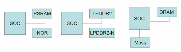
One of the most interesting slides that Floman presented at the JEDEC Mobile Forum, in my opinion, was an image that showed three processor/memory architectures for mobile phones.

The graphic looked like this:


The two architectures on the left are execute-in-place (XIP) architectures. The leftmost architecture employs pseudo-static RAM and NOR Flash as memory and executes operating-system code directly from the NOR Flash memory. The middle architecture replaces the pseudo-static RAM and NOR Flash memory with LPDDR2 SDRAM and LPDDR2-N Non-Volatile Flash memory. It’s still an execute-in-place architecture but the memory components are newer and deliver more performance with better capacity.

The architecture on the right is a shadowing architecture where the OS code is stored in a mass-storage device (NAND Flash memory) and the code is first transferred to DRAM and then executed. High-end smartphones use this architecture.


These architectural designs will hold unless a new type of memory with both fast read/write times and non-volatile storage become commercially available in the required capacities and the required cost per bit. If that happens, the smartphone will only need one memory type—perhaps that might be magnetic RAM (MRAM) or Memristor-based memory. But that’s not the situation today.

The best possible performance, said Floman, will come from Wide I/O DRAM while the UFS (Universal Flash Storage) standard appears to be poised to become the next commonly used storage medium for smartphone design. UFS “will be the next generation mass memory” for smartphones, said Floman.

All of this evolution has but a single purpose. “You will not buy your next phone from the same manufacturer unless it provides new functions,” Floman said as he concluded his keynote speech.

Friday, April 20, 2012

Qualcomm and Nvidia 28 nm Wafers? Shortage...

Last quarter results from Qualcomm show again the impact of Moore's law breaking down. As detailed below, Qualcomm growth this quarter was limited by the supply of 28 nm wafers. Nvidia has been complaining about similar type of issues in the last few months.

It all is really tied to the bigger issues of increasing cost of developing and producing new process technologies. This fact is reducing the number of leading edge fabs.

Fabless companies to ensure their supply will need to share more of the development costs in order to gain higher priorities.


More information on foundries, fabs, and wafer supply is available at Forecasting Wafer Demand: Technology Migration, Bottlenecks (Link includes a chart of wafer demand by IC product type (i.e. DRAM, NAND, NOR, MPU, PLD, etc))

Ron Maltiel

Friday, March 16, 2012

When will Flash Memory Market be 2x of DRAMs

Flash memory has been increasing in popularity due to its shrinking size. There were papers presented at the recent ISSCC 2012 that discussed 128GB Flash NAND using 22-18 nm process technology while DRAM technology is at 4GB using 38 nm process technology (http://www.miracd.com/ISSCC2012/WebAP/PDF/AP_Full.pdf) .

This leads semiconductor companies to switch fabs from DRAM to flash. See "Hynix is switching production at a memory plant in China to churn out NAND flash instead of DRAM chips"


It will not be long before the size of the flash semiconductor chip market will be 2x the DRAM market size.

Thursday, March 15, 2012

Is Resistive RAM (RRAM) The Future Flash Memory?


Below is an overview of Resistive RAM (RRAM) by Bogdan Govoreanu, from IMEC . This new flash memory technolgy is worth watching.


Eli Harrari, Sandisk founder, CEO, and Chairman from its founding until January 2011 in his ISSCC Plenary talk stated that 3D-RRAM " has a real shot at becoming the next big game-changer in the second half of this decade".

Eli Harrari foresaw upcoming changes in non volatile memory. He converted Sandisk from supporting both NOR and NAND flash to only NAND long before other companies saw the upcoming accelerating growth in NAND.

Ron Maltiel


Resistive RAM for next-generation nonvolatile memory
Bogdan Govoreanu, imec Leuven                                               3/12/2012 1:25 PM EDT


Since its introduction in 1988 by Toshiba1, NAND flash nonvolatile memory has undergone an unprecedented growth, becoming one of today’s technology drivers. Although NAND flash memory has scaled to 1x-nm feature sizes, shrinking cell sizes reduce the number of electrons stored on the floating gate. Resistive RAM (RRAM) provides an alternative. In this article, we review the main performance figures of hafnium-oxide (HfO2)-based RRAM cells4 from a scalability perspective, outlining their strengths as well as the main challenges ahead.

A NAND flash nonvolatile memory cell, usually a floating gate transistor, implements the memory function by charge stored on the floating gate. With a charge transfer mechanism onto/from the storage medium that relies on tunneling and a serial (string) architecture, NAND memory features high operating voltages (with associated chip area consumption for the on-chip voltage generation), rather long cell program/erase (P/E) times, and slow read-access times. These drawbacks are, however, compensated for by the very compact array architecture and extremely low energy-consumption-per-bit operation, which eventually enabled fabrication of high-density memory arrays, at low cost and with a chip storage capacity increasing impressively.
During its extraordinary evolution, NAND flash has often met seemingly insurmountable barriers. Technological, architectural, and design innovations complemented each other, however, enabling continued scaling. Nowadays, NAND flash memory seems to have found the way toward the realm of 1x-nm feature size, with major players fighting for each nanometer of cell shrinkage, not to mention for supremacy. Nevertheless, the scaling of cell size leads to gradual reduction of the number of electrons stored on the floating gate, with a projected number of less than 30 electrons for memorizing a (multilevel) cell state, for an assumed 15-nm feature size2.

Resistive RAM (RRAM), just like phase-change memory (PCM), is emerging as a disruptive memory technology, implementing memory function in a resistance (rather than stored charge), the value of which can be changed by switching between a low and a high level. Although the phenomenon of reversible resistance switching has been since the 1960s, recent extensive research in the field has led to the proposition of several concepts and mechanisms through which this reversible change of the resistance state is possible. The distinctive feature of most RRAM concepts3 consists of the localized, filamentary nature of a conductive path formed in an insulating material separating two electrodes (a metal-insulator-metal (MIM) structure), corresponding to the on-, low-resistance state. This attribute was immediately associated with a high scalability potential, beyond the limits currently predicted for flash memory.

Resistive memory structures

Even if many materials reported to date exhibit good resistive switching properties, the success of a future RRAM technology is critically dependent on the ability to integrate these materials/switching structures into a conventional, supporting baseline technology, with cost as a key success factor. Not surprisingly, fab-friendly and accessible materials such as HfO2, zirconium dioxide, titanium dioxide, tantalum dioxide/ditantalum pentoxide, etc, which showed resistive switching behavior, have received the highest attention.

A thin HfO2 dielectric film sandwiched between two metal electrodes was shown to have resistive switching properties, either uni- or bipolar, depending on the materials used as electrodes and on the method to deposit the active (oxide) film. The bipolar operation of HfO2, requiring voltages of opposite polarity to switch on/off the cell, is believed to be due to the formation of conductive paths (filaments) associated with presence of oxygen vacancies (VO), which can be ruptured/restored through oxygen/VO migration under electric field and/or locally enhanced diffusion. The bipolar operation of HfO2 is preferred for its increased immunity to disturbs and over reset. The formation of the filament (forming, or electroforming) is believed to take place along pre-existing weak spots in the oxide, for instance along the grain boundaries in case of a polycrystalline HfO2, which presumably have larger amount of defects and also a higher oxygen diffusivity compared to the bulk of the material.5,6

An alternative approach is to use a metal/oxide material system7 with a reactive (capping) metal, capable of chemically reducing the HfO2. Although a Hf/HfO2 system may seem an obvious choice, selection of hafnium as a cap layer is supported by thermodynamic considerations that indicate a low oxide formation energy, when reducing HfO2. A similar property is found for the titanium/HfO2 case. In the Hf/HfO2 system, hafnium acts as an oxygen buffer layer that allows, under electrical stimuli, the production of oxygen-deficient off-stoichiometric oxide, thus favoring formation of the switching filament. Furthermore, conventional physical vapor deposition (PVD) titanium nitride was used to define the bottom and top electrodes (BE/TE) in a crossbar-patterned configuration.

To achieve best flexibility and controllability of RRAM device operation, the resistive memory structure was connected serially with an nMOS transistor, which acts as a cell selector. Figure 1a shows a top view scanning-electron-microscopy (SEM) picture of a test structure, while high-resolution transmission-electron-microscopy (TEM) cross-sections of the structure along the main directions, visualizing the BE/TE are shown in figure 1b and figure 1c. The smallest fully functional working structures processed4, feature an effective area of around 10 x 10 nm2, defined by the BE width and by the width of the TE/Hf-cap tip resulting after the crossbar patterning.


Figure 1: Top SEM-view of a crossbar resistive element (a) and high-resolution TEM cross-sections of the bottom- (b) and top-electrode (c).


The oxide thickness is the main parameter determining the value of the forming voltage (VF), which is typically the highest voltage and needed only once, to get the RRAM cells ready for operation. In contrast, the Set (on-switching) and Reset (off-switching) voltages are lower and, in a common situation, do not depend on oxide thickness. This difference makes it possible that VF can be then reduced by thinning the oxide layer, without interfering with normal cell operation. Furthermore, aggressive oxide thinning may eventually lead to forming-free operation.

The Set/Reset (S/R) voltages, as well as the levels of the on/off states, turn out to be essentially independent not only of oxide thickness, but also of cell size. Although operating the cell in extreme conditions (i.e. with very deep Reset or strong Set switching) may turn these characteristics invalid, the common situation is consistent with the filamentary nature of the conductive path; furthermore, it supports the model of a partial rupture and restoration of the filament during device operation. Eventually, the oxide thickness corresponding to forming-free operation, confirmed experimentally to be in the range of 2 to 2.5 nm, is indicative of the extent of the ruptured portion of the conductive filament.


Electrical performance and reliability

Given the structure asymmetry induced by the presence of the hafnium layer, the RRAM cells are best operated in bipolar mode with positive polarity on TE for the Set and forming operations and with negative polarity on TE for the Reset operation. In this section, we will discuss the most important performance and reliability figures of the HfO2-based RRAM cells.


Switching speed

To measure switching speed, we used a pulsed operation mode, exemplified here for a Reset switching. Thus, stimuli were applied on the sourceline (SL) and wordline (WL) of the serial 1T1R (1-transistor, 1-resistor) test vehicle, while the response was monitored with a digital oscilloscope on a small series resistance attached to the cell bitline (BL; see figure 2a) . The switching was time-confined to a maximum duration given by the width of the SL pulse, i.e. 10 ns. We carefully designed the experimental setup to minimize the impact of the parasitic elements (e.g. capacitances), having a reasonably short system time constant. The resistive element, initially in the on-state, switches to the off-state quickly, leading to a decrease of the signal within just 3 to 4 ns (see figure 2b). When taking into account the impact of the testing environment on the collected waveform, the observed transition time duration gives a higher margin for the intrinsic switching time, which can be shorter.


Figure 2: Schematics of the device under test (DUT), with applied stimuli and collected response (a) and waveforms corresponding to a Reset switching (b), sampled with a LeCroy WavePro 740Zi 4GHz oscilloscope. The 10-ns SL pulse (blue color), which enables switching, in contained in the longer WL pulse (red color) used to open up the transistor’s channel. The Reset switching is confirmed by the read-out (RO) of the cell current, which changes from high value (on-state) before the SL applied pulse to low value (off-state) after the pulse.


On/off window & operating voltages

The on/off window easily exceeds a factor of 10, with modest (<1 V) voltages applied for both S/R operations. Using higher amplitude pulses and switching verification will improve the on/off window by at least two orders of magnitude, as well as enhancing the uniformity of the switching operations (see figure 3a), which may open up paths for multilevel operation.


Figure 3: Typical on/off window (expressed in read-out cell current) achievable with sub-3-V pulsed operation, with verify (a) and Reset pulse amplitude-duration voltage-time trade-off, showing no significant degradation when scaling cell size from 1 um2 down to 10 x 10 nm2 (b). Data are for an oxide film thickness of 10 nm. The dashed lines are guide for the eye. Similar conclusions hold for Set switching (not shown).


The voltage-time dilemma is a popular term used to express the limited ability of RRAM to display nonlinearity. This is however not specific to RRAM, but present in virtually all memory structures, which ideally need to on one hand allow for indefinitely long stability under no or low-electrical stimuli (for retention, read-out and disturbs immunity), while on the other hand providing fast change of state under operating stimuli (for P/E or S/R).

The S/R voltages required to operate these cells thus display the usual trade-off with time. Nevertheless, the pulse amplitude-time dependence shows that the cells can still be operated with voltages well below 3 V, even for pulses as short as 10 ns. Furthermore, in a comparison of large area cells (in the order of 1 um2) with smallest-size cells (of 10 x 10 nm2), the voltage-time characteristics maintain similarity (see figure 3b), which shows that we should expect no considerable performance degradation when considering aggressively scaled structures. Compared to NAND flash, RRAM has the benefits of low-operating voltages.


Reliability: retention & endurance

The usual 10 year requirement for NVM retention is met by most of the RRAM cells, with a median cell reaching this limit at an extrapolated temperature of around 100°C. As expected, retention turns out to be most critical for the on-state, where retention loss is attributed to filament dissolution. Retention improvement is possible through material optimization and careful sealing of the active region with oxygen-free layers.

Endurance tests performed on unoptimized samples showed cycling of at least 10 Mcycles in a single shot. The failure at the end of the tests was, however, recoverable with a stronger stimulus to “unlock” them from the stuck state, and cycled again with adjusted slightly stronger conditions. These facts suggest that careful balancing of the S/R test conditions, next to process improvement, may allow superior reliability and extended device lifetime, which can well exceed billion cycles, even on the smallest device sizes. This figure is far above the conventional requirement for flash memory, pinpointed to 100 kcycles, although reference value for data storage flash is commonly lowered down 10 kcycles, on arguments of practical, as well as economical nature associated with a commodity product.

Scalability, energy consumption, and cell array considerations

The data discussed so far provide evidence of RRAM operation on an effective area of nearly 10-x-10-nm2 without compromising any of the major performance or reliability figures. This size is the smallest reported to date, for HfO2-based RRAM cells and demonstrate cell scalability in the nanometer range, which is beyond scaling limits of NAND flash. Filament formation has been observed experimentally, for instance on TEM pictures, for metallic filaments, such as those formed in nitrous oxide RRAM.


Figure 4: Extracted filament size for 10-x-10-nm2 cells, operated with 10-ns pulse duration. The filament was asssumed cylindrical, with a saturated sub-stochiometric hafnia resistivity.8


In the cells under discussion here, conductive paths presumably formed by oxygen vacancies corresponding to locally lower fractions of oxygen content in the active oxide layer are hard to detect, due to resolution limits of the physical characterization methods. Oxygen-deficient HfO2, however, has a resistivity that correlates with the amount of oxygen-deficiency, but eventually saturates for highly deficient stable sub-oxides, at a value still significantly higher than that of metallic Hf.8 When combined with experimental electrical data corresponding to on-state (measured on the smallest 10 x 10 nm2 HfO2-based RRAM cells), this property allowed extracting the radius of an assumed-cylindrical filament, with a median value of nearly 1 nm. Although an estimate, this result suggests intrinsic scalability of the resistive memory element in the few-nanometer range.

One of the key features of NAND flash technology is the extremely low power required to write/erase a single cell, as it only involves very low (Fowler-Nordheim) tunneling currents. This translates, in spite of the need to use high P/E voltages, into a low energy used to operate a cell, even with the long specific cell P/E times, thus enabling a high throughput in NAND flash. RRAM, by contrast, works at much lower voltages and on/off switching is several orders of magnitude faster than for NAND cells. The current is, however, significantly larger and even if RRAM scores well in comparison with MRAM9 and PCM technologies10,11 there are concerns about the circuit level implications.


Figure 5: Benchmarking of HfO2-based RRAM in relation with existing (NAND flash) and other emerging technologies (MRAM, PCM). An improvement direction implying use of shorter pulses is identified experimentally.4

When we consider the switching energy per bit operation, RRAM is approaching the performance of NAND flash, given the actual peak current levels during switching as high as a few tens of microamps. Crossing below a 10-fJ-NAND flash border would require nanosecond switching speeds, or sub-microamp switching currents; paths to meeting these requirements are currently pursued.

RRAM has device-level characteristics that meet most of the nonvolatile memory requirements. It furthermore shows scalability potential in an area that is thought to be inaccessible to NAND flash. To be able to exploit these strengths at circuit/system level, RRAM must overcome cell read-out interference12 that may cause in erroneous read out of the (HRS) cell state, due to so-called sneak-current paths. Alleviation of this issue requires a bidirectional selector device. The control transistor in a 1T1R structure provides this functionality and it is, in fact, a potential solution for memory arrays in which density is not the main concern. For data storage applications, however, achieving highest memory density should aim at a cell footprint of around 4F2 (with F being the feature size), implementation of which will, most likely, require the use of a two-terminal selector device13 or a rectification function built into the memory element itself (self-rectifying resistive memory). Research achievements in this direction, complemented by consideration of practical possibilities to increase effective density by using 3D architectures14 for meeting cost effectiveness, will eventually determine the success of RRAM as the future nonvolatile memory of choice.

In summary, HfO2-based RRAM shows great promise for future generation nonvolatile memory, offering a fab-friendly option, with performance characteristics that qualify it for a fast, low-voltage, low-energy-consumption memory, with a good and perfectible reliability, as demonstrated for fully-functional 10-nm-size devices and with inferred intrinsic scalability down to a few-nanometer size. Further improvement in reliability and additional “in-the-footprint” or built-in selection functionality set important milestones ahead on the road to becoming tomorrow’s nonvolatile memory.


Note: This article is based on the work reported at IEDM 2011 by the Emerging Memory Devices Program team of imec Leuven.4


References

1. M. Momodomi et al, IEDM Tech. Dig, pp. 412-415, 1988.

2. K. Prall, Proc. NVSMW, pp. 5-10, 2007.

3. R. Waser, IEDM Tech. Dig, pp. 289-292, 2008.

4. B. Govoreanu et al, IEDM Tech. Dig, pp. 729-732, 2011.

5. G. Bersuker et al, IEDM Tech. Dig, pp. 456-459, 2010.

6. U. Brossmann et al, J.Appl.Phys, 85(11): 7646-7654, 1999.

7. B. Govoreanu et al, Ext. Abstr. SSDM, pp. 1005-1006, 2011.

8. E. Hildebrandt et al, Appl.Phys.Lett, 99: 112902, 2011.

9. K. Tsukida et al, ISSCC Dig, pp. 258-259, 2010.

10. R. Annunziata et al, IEDM Tech. Dig, pp. 97-100, 2010.

11. S.H. Lee et al, IEDM Tech. Dig, pp. 47-50, 2011.

12. M-J. Lee et al, IEDM Tech. Dig, pp. 771-774, 2007.

13. K. Gopalakhrishnan, VLSI Tech. Symp, pp. 205-206.

14. I.-G. Baek, IEDM Tech. Dig, pp. 737-740, 2011.


About the author

Bogdan Govoreanu is currently appointed as a principal scientist with imec Leuven and a staff member of the Memory Device Design Group, Process Technology Unit, carrying out research in the field of emerging memory devices with focus on resistive switching memory. He received his Ph.D.in Applied Sciences in 2004 from the University of Leuven (Katholieke Universiteit Leuven). During his career, Govoreanu has authored or co-authored over 80 research papers and holds/has filed six US and European patents/patent applications. He is also an IEEE Senior Member.