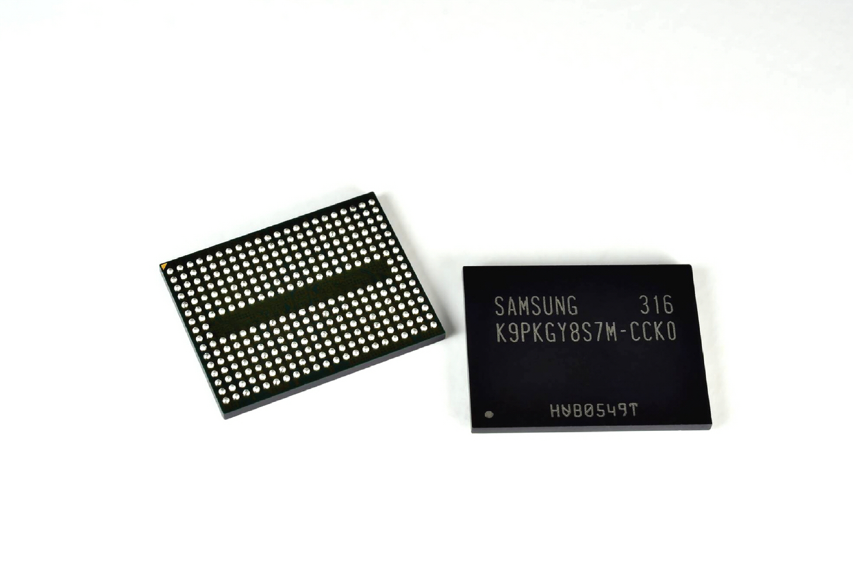
Semiconductor companies have been building 3D devices (which are vertical circuits above the silicon die edge surface) for the last couple years. They have been going in the vertical direction due to the complexity of shrinking the devices (see 2012 Moore's Law Slowwwing ). Samsung has
been making 3D V-NAND since 2013 (see Samsung’s 1Tb SSD: 3D Vertical NAND ). Samsung is now using
its vertical layer manufacturing know-how to increase its market share in V-NAND and DRAM.
More about Samsung's progress below.
Ron
Insightful, timely, and accurate semiconductor
consulting.
SEOUL (Reuters) - Gloom may be settling over
much of the world's semiconductor industry but Samsung Electronics Co Ltd is
expected to cope better than most due to its strong technological edge,
enabling it to boost market share for some key products and possibly even lift
revenue.
A plunge in PC sales and slower growth for
smartphones globally has hit the sector hard, prompting Intel Corp to say this
month it would cut up to 12,000 jobs.
Qualcomm has said fiscal third-quarter chip
shipments could fall as much as 22 percent, while SK Hynix Inc on Tuesday
reported a 65 percent slide in quarterly operating income - its weakest result
in three years.
Samsung, which reports its first-quarter
earnings on Thursday, is also hurting. Chip profits - which accounted for just
under half of its overall 2015 operating income - are widely expected to fall,
with some analysts predicting a drop of more than 10 percent in January-March
from a year earlier.
But if its rivals are getting pummeled, the
South Korean tech giant is merely bruised and is in many ways benefiting as
clients shift towards premium power-conserving DRAM chips for smartphones, as
well as solid-state drives for data storage using 3D NAND chips.
"The technological gap between Samsung and
its competitors in fields such as DRAM and NAND has been widening lately, which
helps the company avoid the rate of profit decline seen at other firms,"
said Song Myung-sub, an analyst at HI Investment & Securities.
Even with a first-quarter drop of around 10
percent, Samsung's chip operating profit is expected to be nearly five times
that of SK Hynix.
The world's No. 2 chipmaker also happens to run
the world's biggest smartphone business, giving it a captive customer for its
chips that none of its rivals have.
"This is a safehouse they can go to,"
said Avril Wu, an analyst at research firm Trendforce.
Healthy initial sales for Samsung's new
flagship Galaxy S7 smartphones are expected to be the main driver of
first-quarter operating profit, which the firm has said likely rose 10.4
percent from a year earlier to 6.6 trillion won ($5.8 billion).
DOMINANT POSITION
Of its key products, analysts are most upbeat
about Samsung's NAND chip prospects. Samsung was the first to mass produce NAND
flash chips using a technology called 3D NAND, helping it assume a dominant
position in higher-margin products such as solid-state hard drives for
computers and servers.
BNP Paribas expects the South Korean firm's
NAND revenue to climb 16 percent and NAND operating profit to jump 69 percent
this year. Shipments will also likely outpace the industry average, allowing
Samsung to seize more market share, it said in a report.
The technology is already contributing to
Samsung's profits, analysts say, adding that this is not the case for main NAND
rivals Toshiba Corp, SK Hynix and Micron Technology Inc which are estimated to
be as much as three years behind.
Investors and analysts also point to Samsung's
superior production technology for DRAM chips, saying the firm is ahead of its
closest rivals by at least a year. It can mass produce smaller chips than
rivals, which boosts performance and conserves power as well as increasing the
number that can be made from a single wafer.
Samsung commanded 58 percent of the mobile DRAM
market as of the fourth quarter of 2015, according to TrendForce. Mobile DRAM
revenue also accounted for more than half of Samsung's overall DRAM sales for
October-March, TrendForce's data shows.
(Reporting by Se Young Lee; Editing by Edwina
Gibbs)
Ron Insightful, timely, and accurate semiconductor consulting. Semiconductor information and news at - http://www.maltiel-consulting.com/
IBM officially biggest all-flash array
shipper - analyst
Gartner AFA data hits the street
By Chris Mellor, 13 Jun 2014
No,
it isn’t the greatly anticipated all-flash array magic quadrant, but it's great
Gartner analysis nonetheless. The number-crunchers at Gartner HWQ have produced
a Market Share Analysis: SSDs and Solid-State Arrays, Worldwide, 2013. Yummy.
Let’s see what’s inside.
The
doc, available as a download from Pure Storage (guess who's
done well in the analysis) after registering a few details. It looks at both
SSDs and all-flash arrays, which Gartner calls Solid State Arrays (SSAs) and
IBM comes out as the leading SSA shipper – with Pure Storage second.
SSAs
are defined carefully: ”SSAs are scalable, dedicated, solutions based solely on
solid-state semiconductor technology for data storage that cannot be configured
with HDD technology at any time. As distinct from SSD-only racks within ECB
storage arrays, an SSA must be a stand-alone product denoted with a specific
name and model number, which typically (but not always) includes an operating
system and data management software optimised for solid-state technology.”
To
cut a long story short, Dell and HDS all-flash array products are excluded, as
are all-flash versions of – for example – EMC VMAX and VNX, and NetApp FAS
arrays.
The
SSD category embraces PCIe flash cards and also includes “self-contained
solid-state NAND dual in-line memory modules (DIMMs), which must be used in dedicated
slots in servers. Mainstream PC SSDs being used in servers are counted in this
category due to end consumption.”
We’ll
graph the information here, and you can read the detailed numbers by
downloading the doc. The SSD info starts with worldwide vendor revenues:
Click chart for larger version
Total
SSD revenues in 2012 were $7.2 billion, and in 2013 had risen to $10.99
billion, a 53.1 per cent increase.
Samsung
as top dog got most of that with Intel, growing less, at number 2. Look at
Sandisk’s rocketing growth up into the no 3 slot, closely followed by Micron.
Toshiba held its fifth place but didn’t grow much. WD grew, Fusion-io declined
and now we’re in the tail-enders.
Now
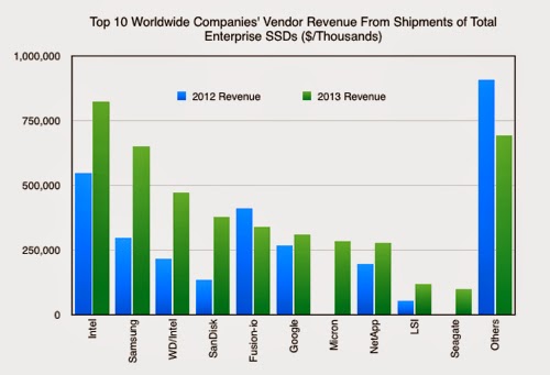
let’s look at the enterprise SSD market:
Intel
is top dog, not second-placed Samsung. WD, with its HGST/Intel SSDs is in third
place followed by SanDisk successfully exhibiting its enterprise supplier
credentials. Then there’s Fusion-io, which declined 2012 - 2013, Google with
its internal use - amazing - Micron is a, we think, in a disappointing sixth
place, NetApp a, for it, strong seventh then LSI and Seagate. EMC does not
appear at all.
Now
for the SSA numbers.
Here
are the vendor revenue market share numbers:
Click chart to make it larger.
And
here the actual SSA revenues by vendor:
Click chart to make it larger
IBM
has had a wildly successful 2013 year, solidly overtaking Violin Memory to
claim a dominating number 1 slot. Pure Storage has rocketed to the number 2
position in 2013 while Violin Memory slumped from first place in 2013 to third
in 2013, illustrating the new management team’s uphill task. EMC has sprung
into fourth place from a standing start and NetApp is not far behind in the
fifth slot. Then there’s Nimbus Data and tail-ender Cisco - a dismal showing
for the networking behemoth in our view, with startup SolidFire very close
behind.
The
SSA market was sized by Gartner at $236.5m in 2012, and 182.1 per cent higher
at $667.3m in 2013. IBM’s SSA revenues grew at 278.1 per cent, Pure's at a
magnificent 642.3 per cent and no other vendor outpaced the market, meaning
they lost share.
Now
this is artificial, as EMC, Kaminario, SolidFire and HP had no presence in
Gartner’s numbers in 2013, but we can assert that Violin Memory, NetApp, Nimbus
and Cisco all lost share from 2012 to 2013. With EMC, Kaminario, SolidFire and
HP now in the SAA market we might expect these losses to continue in 2014.
The
Gartner analysis contains more data, segment metrics and so forth. It’s worth a
download and read if you’re interested.
Main takeaway? Big Blue
really is big in SSAs, Pure Storage is living up to its hype, and the SSA
market is growing at a fast lick. NAND the story goes on
Many computer memory chipmakers worldwide are said to be working to enlarge plants that produce NAND flash memory chips.
According to the San Kei Shimbun on May 12, Toshiba, the world’s second-largest NAND flash memory chipmaker, decided to make an investment in a 3D V-NAND flash memory production facility in partnership with US-based semiconductor company SanDisk. Both companies are going to equally share the cost of the investment and inject 700 billion yen (7.419 trillion won, US$6.843 billion) for three years at the Yokkaichi Operation plant, the company’s memory production facility in Mie prefecture, Japan. At first, they estimated the amount at 400 billion yen. However, it nearly doubled after the two firms agreed to invest in the construction of a new facility and the replacement of the existing one.
An increase in investment can be interpreted as Toshiba’s willingness to not lag behind its rival companies like Samsung Electronics, SK Hynix, and Micron. Given that Samsung completed the construction of its 3D V-NAND production facility in Xian, China on May 9, competition between Korean and Japanese firms to dominate the next-gen semiconductor memory market is expected to heat up again.
Samsung began to mass-produce 3D V-NAND flash memory chips in its plant in Xian. 3D V-NAND flash memory where 40nm-class NAND flash memory is stacked up in 24 layers are twice as fast and last 10 times longer than 20nm-class planar NAND flash memory. The world’s largest computer memory chipmaker is planning to dominate the market by developing 3D V-NAND flash memory chips in a 36-layer stack soon.
SK Hynix, the world's fourth-largest manufacturer of computer memory chips, is focusing on investing in NAND flash memory. For example, the firm converted its Cheongju M12 Plant that produced both DRAM and NAND flash memory chips into a NAND flash line last year in order to restructure the company whose focus was on DRAM. The chip-maker plans to mass-produce 3D V-NAND at the end of this year. Micron, which is in the third spot, recently changed its DRAM factory in Singapore into a NAND flash plant.
Unlike its rivals, Toshiba only manufacturers NAND flash memory. Therefore, if competitors outperform the Japanese firm in the global NAND flash memory market, it will be fatal. Industry analysts are saying that Toshiba's lawsuit filed in March against SK Hynix for technology leakage despite its patent cross-licensing deal with the Korean firm was aimed at checking the Korean chip-maker's influence.
According to the findings of market research firm IHS Technology, sales of NAND flash memory worldwide is estimated at US$25.8 billion last year, and the market continues to grow rapidly. In 2013, Samsung was the world's number one seller of computer memory chips with a 34.7 market share, followed by Toshiba (a 32.2 market share).
Below are some snapshot from Ifixit teardown of Google/ Motorola new cell phone. One of the key features of Motorola cell phones have been their very long battery life. Is it due to the combination of Qualcomm processor and the power management chip, some of the other chips, or their custom system architecture (software/ hardware)?
The key chips in Moto X are listed below.
Ron Insightful, timely, and accurate semiconductor consulting. Semiconductor information and news at - http://www.maltiel-consulting.com/
The love child of Motorola and Google is here, and we are dying to crack open the little Motoroogle.
Technical Specifications:
Dual-core 1.7 GHz Qualcomm Snapdragon S4 Pro processor
2 GB RAM
4.7-inch 1280x720 pixels AMOLED display
16 or 32 GB internal storage
Qualcomm Adreno 320 GPU
.........
Step 9
Motorola claims the Moto X battery can power through an amazing 24 hours of "mixed usage."
How does the Moto X accomplish such a feat with a 3.8 volt, 2200 mAh Lithium ion battery? The secret is in the X8 Mobile Computing System.
The Motorola X8 Mobile Computing System is comprised of a Qualcomm Snapdragon S4Pro family processor, a natural language processor and a contextual computing processor.
Motorola developed a custom system architecture, which, when coupled with eight processor cores, allows for the delegation of processing power:
4 graphics processor cores for "stunning clarity"
2 application processor cores for "swift action"
2 low-power cores—"awaiting your next command"
Step 10
Out comes the upper midframe panel, housing the speaker, headphone jack, more antennas, and pressure contacts.
Yay, pressure contacts!We like spring pressure contacts because they don't require any work to disconnect.
This is possibly the most modular headphone jack we've ever seen. It pops right out of the upper midframe panel, spring contacts and all.
Texas InstrumentsTMS320C55Digital Signal Processor
NXP 44701 NFC Chip
Skyworks77619-12Multiband Multimode Power Amplifier Module for Quad-Band GSM / EDGE and Penta-Band (Bands I, II, IV, V, VIII) WCDMA/ HSDPA/ HSUPA/ HSPA+/ LTE
Texas InstrumentsMSP430 F5259Mixed Signal Microcontroller
Yesterday Samsung announced 3D flash V-NAND at Flash Summit
A key advantage of 3D vertical scaling is that device and process development issues of silicon based technology are better understood than other future flash approaches that depends on integrating brand new materials.
Two other strong flash vendors are also developing 3D Flash
Based on Samsung keynote announcement at the flash summit:
1. Samsung is having already engineering sample now and it will be in production in 2014.
2. Unless there is some unexpected development, it sound like Samsung's 3D NAND (and similar flavors by its competitors) will be the mainstream future NAND technology.
3. A key issue which they did not explain is erase cycle. They only said that erase had to be optimized with specific circuits.
6. The first 3D test product they made was 16G in 2011, the current one is 128Gb which is built using a stack of 24 layers.
7. Samsung is building it based on a standard known 30nm silicon technology, they said it is cost competitive (or cheaper?) than planar technology. I am not sure what are their assumptions are as far as cost, but they are probably correct that it will be cheaper than competing future technologies.
Ron Insightful, timely, and accurate semiconductor consulting. Semiconductor information and news at - http://www.maltiel-consulting.com/
The article below discuss using CTF instead of floating gate to create 3D flash memory with up to 1T SSD product next year.
" new V-NAND is manufactured at a 10nm process size, and it starts at a density of 128Gb per NAND chip. The NAND chips are constructed in layers, stacking up to 24 individual NAND cells on top of each other...
Samsung is claiming that at minimum, the CTF-based V-NAND has at least a 2x increase in lifespan over floating gate NAND, and perhaps as high as 10x. Additionally, write performance is doubled over floating gate NAND."
Already in 2006 Samsung discussed CTF memory cell for NAND chips CTF for 40nm 32Gb .
Longer life, higher reliability, more performance—what's not to like?
by Lee Hutchinson - Aug 6 2013, 7:50am PDT
SSD enthusiasts know all about SLC, MLC, and TLC, but there are some new acronyms in SSD town: V-NAND and CTF. Samsung announced in a press release last night that it has begun mass production of "3D Vertical NAND," a type of flash that it claims overcomes the existing limits on the design and production of existing NAND types. When we looked at those limits about a year ago, they seemed pretty significant; Samsung's V-NAND aims to neatly sidestep most of the issues.
Enlarge/ Samsung's 3D Vertical NAND stacks up to 24 NAND elements on top of each other.
The new V-NAND is manufactured at a 10nm process size, and it starts at a density of 128Gb per NAND chip. The NAND chips are constructed in layers, stacking up to 24 individual NAND cells on top of each other. This lets S amsung scale the chip's capacity up without having to add more NAND cells in a series, or "planar scaling," as the traditional "just shrink 'em and add more cells" method is called.
The other acronym, CTF, stands for "Charge Trap Flash." Traditional NAND flash records zeros and ones by storing charge in a set of floating gate transistors, with the presence or absence of charge corresponding to a 0 or a 1 in single-level cell NAND, and the amount of charge corresponding to different multibit values in multi- and triple-level cell NAND (we have an extremely in-depth primer on the inner workings of SSDs if you want more details). However, Samsung's new V-NAND dispenses with floating gate transistors and uses a different method:
Samsung's CTF-based NAND flash architecture, an electric charge is temporarily placed in a holding chamber of the non-conductive layer of flash that is composed of silicon nitride (SiN), instead of using a floating gate to prevent interference between neighboring cells.
The longevity and reliability problems with standard floating gate transistor-based NAND have a lot to do with the large amounts of power required to perform erasures. Without taking too large a digression, each time a NAND transistor undergoes a program/erase cycle, it retains some additional electrons in its dielectric layer. Eventually, these trapped electrons alter the transistor's resistance to the point that it can no longer be reliably read. The problem grows worse as the NAND cell manufacturing process shrinks—smaller cells become useless at lower levels of retained charge.
Smaller NAND transistor gates means it takes a smaller retained charge to overwhelm the gates' ability to quickly and reliably change state.
Aurich Lawson
The switch from floating gate to Charge Trap Flash appears to negate a lot of these issues. Samsung is claiming that at minimum, the CTF-based V-NAND has at least a 2x increase in lifespan over floating gate NAND, and perhaps as high as 10x. Additionally, write performance is doubled over floating gate NAND.
Samsung predicts that V-NAND will scale up to 1Tb per individual NAND chip. Most SSDs use at least eight NAND chips in parallel, so V-NAND could lead directly to low dollar-per-GB 2.5-inch form factor SSDs of 1TB and beyond—capacities which many Ars commenters have said repeatedly that they desperately want. At that size, concerns over installing an operating system and a few games on a fast SSD and stashing non-speed-critical files on a larger HDD are moot, and most folks can simply use the SSD exclusively without worry. There's no word yet on exactly when a consumer-level SSD filled with V-NAND will become available, but Samsung's vertical integration likely means that the first V-NAND SSD will be a Samsung-branded product with a Samsung-branded SSD controller.