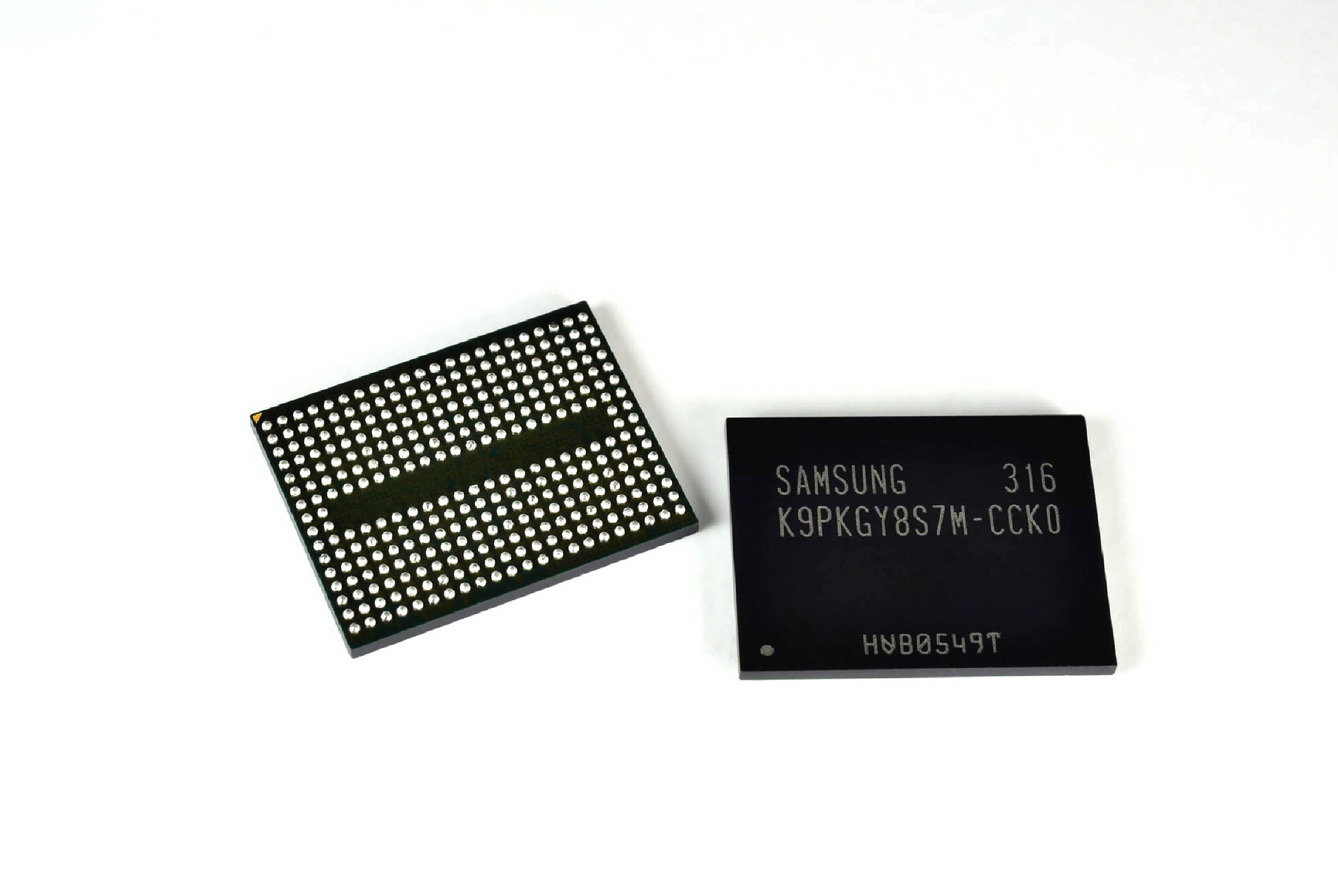
Semiconductor companies have been building 3D devices (which are vertical circuits above the silicon die edge surface) for the last couple years. They have been going in the vertical direction due to the complexity of shrinking the devices (see 2012 Moore's Law Slowwwing ). Samsung has
been making 3D V-NAND since 2013 (see Samsung’s 1Tb SSD: 3D Vertical NAND ). Samsung is now using
its vertical layer manufacturing know-how to increase its market share in V-NAND and DRAM.
More about Samsung's progress below.
Ron
Insightful, timely, and accurate semiconductor
consulting.
SEOUL (Reuters) - Gloom may be settling over
much of the world's semiconductor industry but Samsung Electronics Co Ltd is
expected to cope better than most due to its strong technological edge,
enabling it to boost market share for some key products and possibly even lift
revenue.
A plunge in PC sales and slower growth for
smartphones globally has hit the sector hard, prompting Intel Corp to say this
month it would cut up to 12,000 jobs.
Qualcomm has said fiscal third-quarter chip
shipments could fall as much as 22 percent, while SK Hynix Inc on Tuesday
reported a 65 percent slide in quarterly operating income - its weakest result
in three years.
Samsung, which reports its first-quarter
earnings on Thursday, is also hurting. Chip profits - which accounted for just
under half of its overall 2015 operating income - are widely expected to fall,
with some analysts predicting a drop of more than 10 percent in January-March
from a year earlier.
But if its rivals are getting pummeled, the
South Korean tech giant is merely bruised and is in many ways benefiting as
clients shift towards premium power-conserving DRAM chips for smartphones, as
well as solid-state drives for data storage using 3D NAND chips.
"The technological gap between Samsung and
its competitors in fields such as DRAM and NAND has been widening lately, which
helps the company avoid the rate of profit decline seen at other firms,"
said Song Myung-sub, an analyst at HI Investment & Securities.
Even with a first-quarter drop of around 10
percent, Samsung's chip operating profit is expected to be nearly five times
that of SK Hynix.
The world's No. 2 chipmaker also happens to run
the world's biggest smartphone business, giving it a captive customer for its
chips that none of its rivals have.
"This is a safehouse they can go to,"
said Avril Wu, an analyst at research firm Trendforce.
Healthy initial sales for Samsung's new
flagship Galaxy S7 smartphones are expected to be the main driver of
first-quarter operating profit, which the firm has said likely rose 10.4
percent from a year earlier to 6.6 trillion won ($5.8 billion).
DOMINANT POSITION
Of its key products, analysts are most upbeat
about Samsung's NAND chip prospects. Samsung was the first to mass produce NAND
flash chips using a technology called 3D NAND, helping it assume a dominant
position in higher-margin products such as solid-state hard drives for
computers and servers.
BNP Paribas expects the South Korean firm's
NAND revenue to climb 16 percent and NAND operating profit to jump 69 percent
this year. Shipments will also likely outpace the industry average, allowing
Samsung to seize more market share, it said in a report.
The technology is already contributing to
Samsung's profits, analysts say, adding that this is not the case for main NAND
rivals Toshiba Corp, SK Hynix and Micron Technology Inc which are estimated to
be as much as three years behind.
Investors and analysts also point to Samsung's
superior production technology for DRAM chips, saying the firm is ahead of its
closest rivals by at least a year. It can mass produce smaller chips than
rivals, which boosts performance and conserves power as well as increasing the
number that can be made from a single wafer.
Samsung commanded 58 percent of the mobile DRAM
market as of the fourth quarter of 2015, according to TrendForce. Mobile DRAM
revenue also accounted for more than half of Samsung's overall DRAM sales for
October-March, TrendForce's data shows.
(Reporting by Se Young Lee; Editing by Edwina
Gibbs)
Below are some snapshot from Ifixit teardown of Google/ Motorola new cell phone. One of the key features of Motorola cell phones have been their very long battery life. Is it due to the combination of Qualcomm processor and the power management chip, some of the other chips, or their custom system architecture (software/ hardware)?
The key chips in Moto X are listed below.
Ron Insightful, timely, and accurate semiconductor consulting. Semiconductor information and news at - http://www.maltiel-consulting.com/
The love child of Motorola and Google is here, and we are dying to crack open the little Motoroogle.
Technical Specifications:
Dual-core 1.7 GHz Qualcomm Snapdragon S4 Pro processor
2 GB RAM
4.7-inch 1280x720 pixels AMOLED display
16 or 32 GB internal storage
Qualcomm Adreno 320 GPU
.........
Step 9
Motorola claims the Moto X battery can power through an amazing 24 hours of "mixed usage."
How does the Moto X accomplish such a feat with a 3.8 volt, 2200 mAh Lithium ion battery? The secret is in the X8 Mobile Computing System.
The Motorola X8 Mobile Computing System is comprised of a Qualcomm Snapdragon S4Pro family processor, a natural language processor and a contextual computing processor.
Motorola developed a custom system architecture, which, when coupled with eight processor cores, allows for the delegation of processing power:
4 graphics processor cores for "stunning clarity"
2 application processor cores for "swift action"
2 low-power cores—"awaiting your next command"
Step 10
Out comes the upper midframe panel, housing the speaker, headphone jack, more antennas, and pressure contacts.
Yay, pressure contacts!We like spring pressure contacts because they don't require any work to disconnect.
This is possibly the most modular headphone jack we've ever seen. It pops right out of the upper midframe panel, spring contacts and all.
Texas InstrumentsTMS320C55Digital Signal Processor
NXP 44701 NFC Chip
Skyworks77619-12Multiband Multimode Power Amplifier Module for Quad-Band GSM / EDGE and Penta-Band (Bands I, II, IV, V, VIII) WCDMA/ HSDPA/ HSUPA/ HSPA+/ LTE
Texas InstrumentsMSP430 F5259Mixed Signal Microcontroller
The article below discuss using CTF instead of floating gate to create 3D flash memory with up to 1T SSD product next year.
" new V-NAND is manufactured at a 10nm process size, and it starts at a density of 128Gb per NAND chip. The NAND chips are constructed in layers, stacking up to 24 individual NAND cells on top of each other...
Samsung is claiming that at minimum, the CTF-based V-NAND has at least a 2x increase in lifespan over floating gate NAND, and perhaps as high as 10x. Additionally, write performance is doubled over floating gate NAND."
Already in 2006 Samsung discussed CTF memory cell for NAND chips CTF for 40nm 32Gb .
Longer life, higher reliability, more performance—what's not to like?
by Lee Hutchinson - Aug 6 2013, 7:50am PDT
SSD enthusiasts know all about SLC, MLC, and TLC, but there are some new acronyms in SSD town: V-NAND and CTF. Samsung announced in a press release last night that it has begun mass production of "3D Vertical NAND," a type of flash that it claims overcomes the existing limits on the design and production of existing NAND types. When we looked at those limits about a year ago, they seemed pretty significant; Samsung's V-NAND aims to neatly sidestep most of the issues.
Enlarge/ Samsung's 3D Vertical NAND stacks up to 24 NAND elements on top of each other.
The new V-NAND is manufactured at a 10nm process size, and it starts at a density of 128Gb per NAND chip. The NAND chips are constructed in layers, stacking up to 24 individual NAND cells on top of each other. This lets S amsung scale the chip's capacity up without having to add more NAND cells in a series, or "planar scaling," as the traditional "just shrink 'em and add more cells" method is called.
The other acronym, CTF, stands for "Charge Trap Flash." Traditional NAND flash records zeros and ones by storing charge in a set of floating gate transistors, with the presence or absence of charge corresponding to a 0 or a 1 in single-level cell NAND, and the amount of charge corresponding to different multibit values in multi- and triple-level cell NAND (we have an extremely in-depth primer on the inner workings of SSDs if you want more details). However, Samsung's new V-NAND dispenses with floating gate transistors and uses a different method:
Samsung's CTF-based NAND flash architecture, an electric charge is temporarily placed in a holding chamber of the non-conductive layer of flash that is composed of silicon nitride (SiN), instead of using a floating gate to prevent interference between neighboring cells.
The longevity and reliability problems with standard floating gate transistor-based NAND have a lot to do with the large amounts of power required to perform erasures. Without taking too large a digression, each time a NAND transistor undergoes a program/erase cycle, it retains some additional electrons in its dielectric layer. Eventually, these trapped electrons alter the transistor's resistance to the point that it can no longer be reliably read. The problem grows worse as the NAND cell manufacturing process shrinks—smaller cells become useless at lower levels of retained charge.
Smaller NAND transistor gates means it takes a smaller retained charge to overwhelm the gates' ability to quickly and reliably change state.
Aurich Lawson
The switch from floating gate to Charge Trap Flash appears to negate a lot of these issues. Samsung is claiming that at minimum, the CTF-based V-NAND has at least a 2x increase in lifespan over floating gate NAND, and perhaps as high as 10x. Additionally, write performance is doubled over floating gate NAND.
Samsung predicts that V-NAND will scale up to 1Tb per individual NAND chip. Most SSDs use at least eight NAND chips in parallel, so V-NAND could lead directly to low dollar-per-GB 2.5-inch form factor SSDs of 1TB and beyond—capacities which many Ars commenters have said repeatedly that they desperately want. At that size, concerns over installing an operating system and a few games on a fast SSD and stashing non-speed-critical files on a larger HDD are moot, and most folks can simply use the SSD exclusively without worry. There's no word yet on exactly when a consumer-level SSD filled with V-NAND will become available, but Samsung's vertical integration likely means that the first V-NAND SSD will be a Samsung-branded product with a Samsung-branded SSD controller.
"Diablo’s Memory Channel Storage (MCS) architecture, expected to show up in servers shipping later this year, allows flash storage components to plug into the super-fast channel now used to connect CPUs with memory. That will slash data-access delays even more than current flash caching products that use the PCI Express bus...
Diablo estimates that MCS can reduce latencies by more than 85 percent compared with PCI Express SSDs (solid-state disks)...
The connection is designed to be used by many DIMMs (dual in-line memory modules) in parallel, so each component doesn’t have to relinquish the bus for another one to use it. That saves time, as well as CPU cycles that would otherwise be used managing the bus"
Ron Insightful, timely, and accurate semiconductor consulting. Semiconductor information and news at - http://www.maltiel-consulting.com/
In the ongoing quest for faster access to data, Diablo Technologies has taken what could be a significant next step.
Diablo’s Memory Channel Storage (MCS) architecture, expected to show up in servers shipping later this year, allows flash storage components to plug into the super-fast channel now used to connect CPUs with memory. That will slash data-access delays even more than current flash caching products that use the PCI Express bus, according to Kevin Wagner, Diablo’s vice president of marketing.
The speed gains could be dramatic, according to Diablo, helping to give applications such as databases, big data analytics and virtual desktops much faster access to the data they need most. Diablo estimates that MCS can reduce latencies by more than 85 percent compared with PCI Express SSDs (solid-state disks). Alternatively, the flash components could be used as memory, making it affordable to equip servers terabytes of memory, Wagner said.
Other than on-chip cache, the memory channel is the fastest route to a CPU, Wagner said. Not only do bits fly faster over this link, there are also no bottlenecks under heavy use. The connection is designed to be used by many DIMMs (dual in-line memory modules) in parallel, so each component doesn’t have to relinquish the bus for another one to use it. That saves time, as well as CPU cycles that would otherwise be used managing the bus, Wagner said.
The parallel design of the memory bus also lets system makers scale up the amount of flash in a server without worrying about diminishing returns, he said. A second MCS flash card will truly double performance, where an added PCIe SSD could not, Wagner said.
Diablo, which has been selling memory controllers for about 10 years, has figured out a way to use the standard DDR-3 interface and protocols to connect flash instead of RAM to a server’s CPU. Flash is far less expensive than RAM, but also more compact. The MCS components, which come in 200GB and 400GB sizes, will fit into standard DIMM slots that typically accommodate just 32GB or so of memory. The only adaptation manufacturers will need to make is adding a few lines of code to the BIOS, Wagner said.
Enterprises are more likely to use MCS as high-capacity memory than as low-latency storage, said analyst Jim Handy of Objective Analysis.
“Having more RAM is something that a lot of people are going to get very excited about,” Handy said. His user surveys show most IT departments automatically get as much RAM as they can for their servers, because memory is where they can get the fastest access to data, Handy said.
“Basically, you’d like everything to be in the RAM,” Handy said. Virtualized data centers, where many servers need to share a large set of data, need a shared store of data. But in other applications, especially with databases and online transaction processing, storage is just a cheaper and more plentiful—but slower—alternative to memory. “Everything that’s on the storage is there just because it can’t fit on the RAM,” he said.
To implement the MCS architecture, Diablo developed software and a custom ASIC (application-specific integrated circuit), which it will sell to component vendors and makers of servers and storage platforms. Flash vendor Smart Storage Systems, which earlier this month agreed to be acquired by SanDisk, will be among the companies using the MCS technology, Wagner said. In addition, a tier-one server vendor is preparing about a dozen server models with the technology and will probably ship the first of them this year, Walker said.
For the most part, Diablo doesn’t expect consumers or small enterprises to install MCS flash on their own computers. However, Diablo may work directly with enterprises that have very large data centers they want to accelerate, he said.
Using MCS flash to supplement DRAM would dramatically reduce the per-gigabyte cost of memory but also would allow for further consolidation of the servers in a data center, Wagner said. A large social networking company with 25,000 servers analyzed the MCS technology and said it would make it possible to do the same amount of work with just 5,000 servers.
That’s because the current DRAM-only servers can be equipped with just 144GB of memory, but MCS would allow each server to have 16GB of DRAM and 800GB of flash. With that much memory, each server can do more work so fewer are needed, Wagner said. Fewer servers would mean savings of space and energy, which would translate into lower costs, he said.
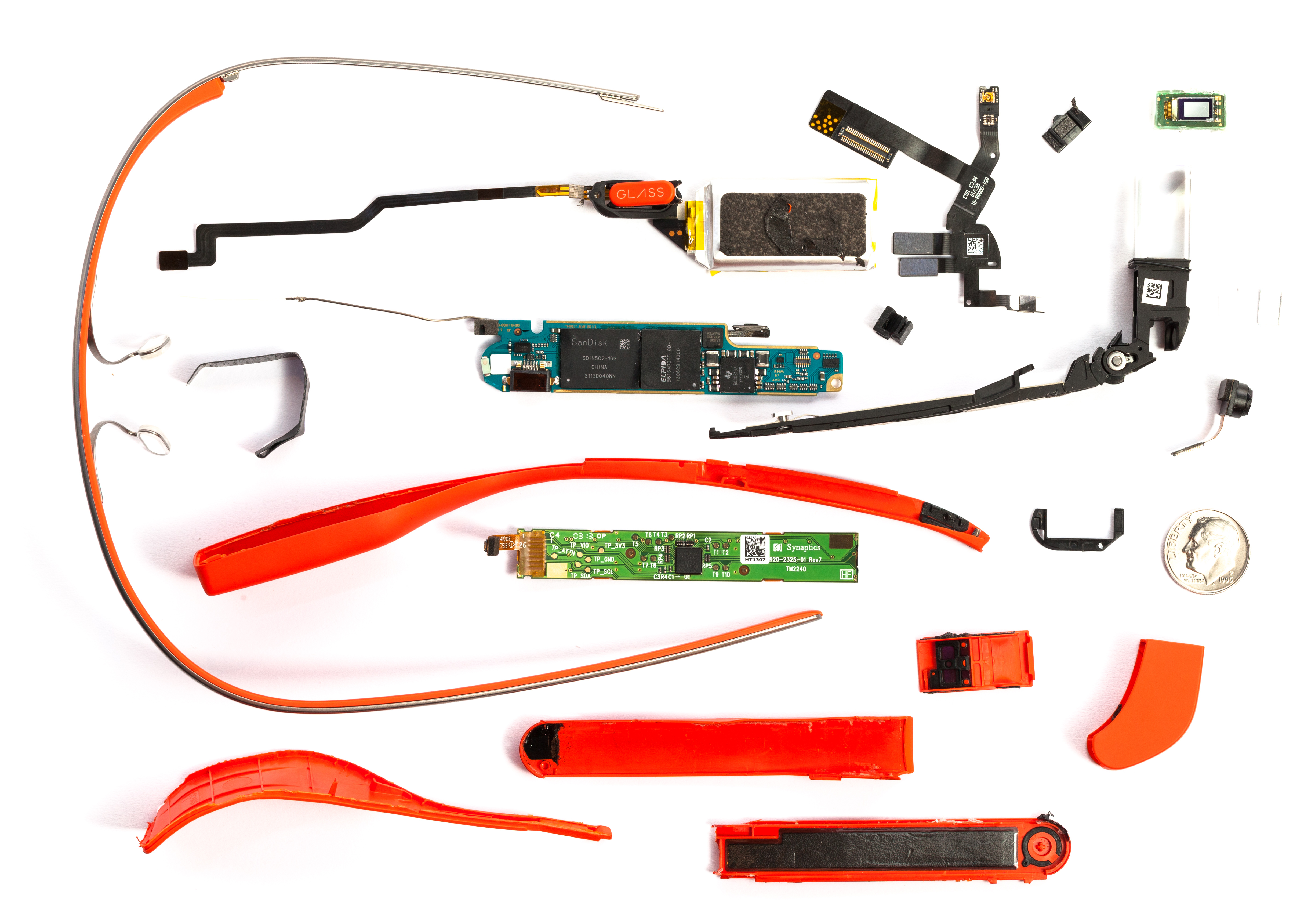
Some highlights of teardown of google glass below.
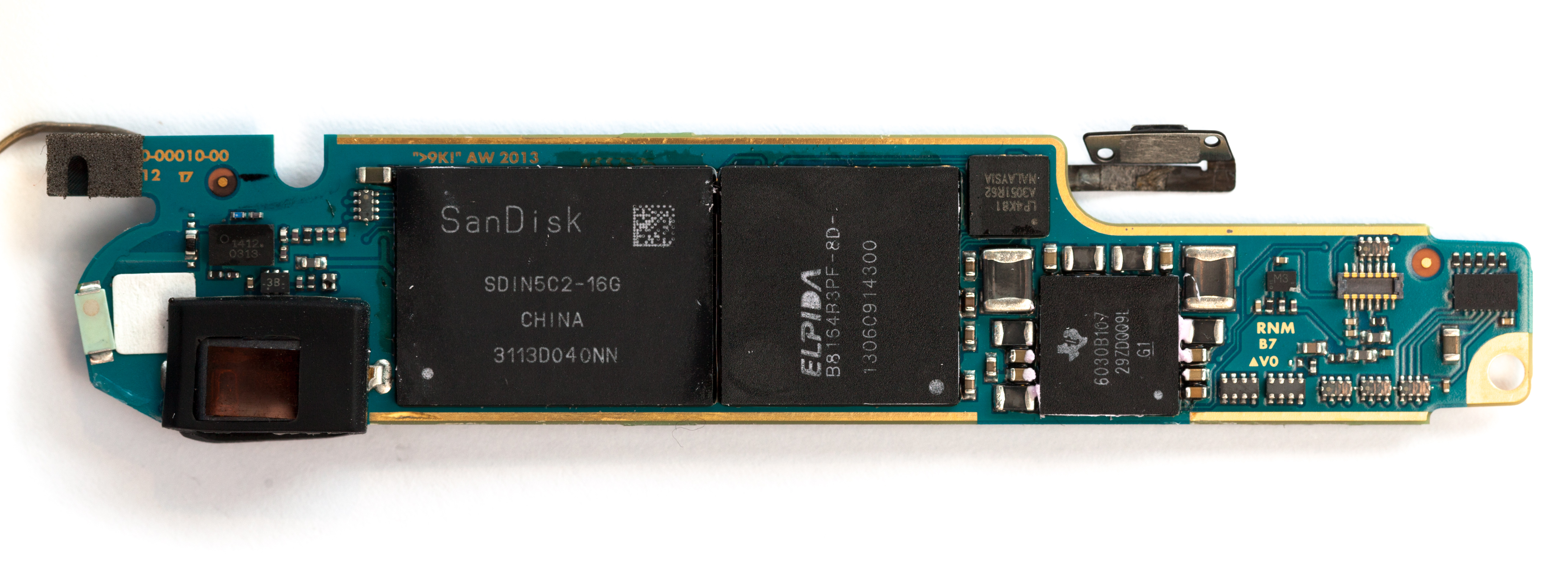
"core chips powering Glass: a TI OMAP4430, 16GB of SanDisk flash, and an Elpida mobile DRAM chip."
Ron Insightful, timely, and accurate semiconductor consulting. Semiconductor information and news at - http://www.maltiel-consulting.com/
What's Inside Google Glass?
What is this Glass thing anyways?
Google's latest and hottest gadget needs little introduction.
Since its public unveiling in April 2012, the tiny head-mounted
Android computer has been collecting controversy and sociological
analysis. It is currently available in limited beta to eminent members
of the tech community and to a selection of "Glass Explorers". As
members of the latter program, we are delighted to be able to explore Glass.
.......
Side Touchpad
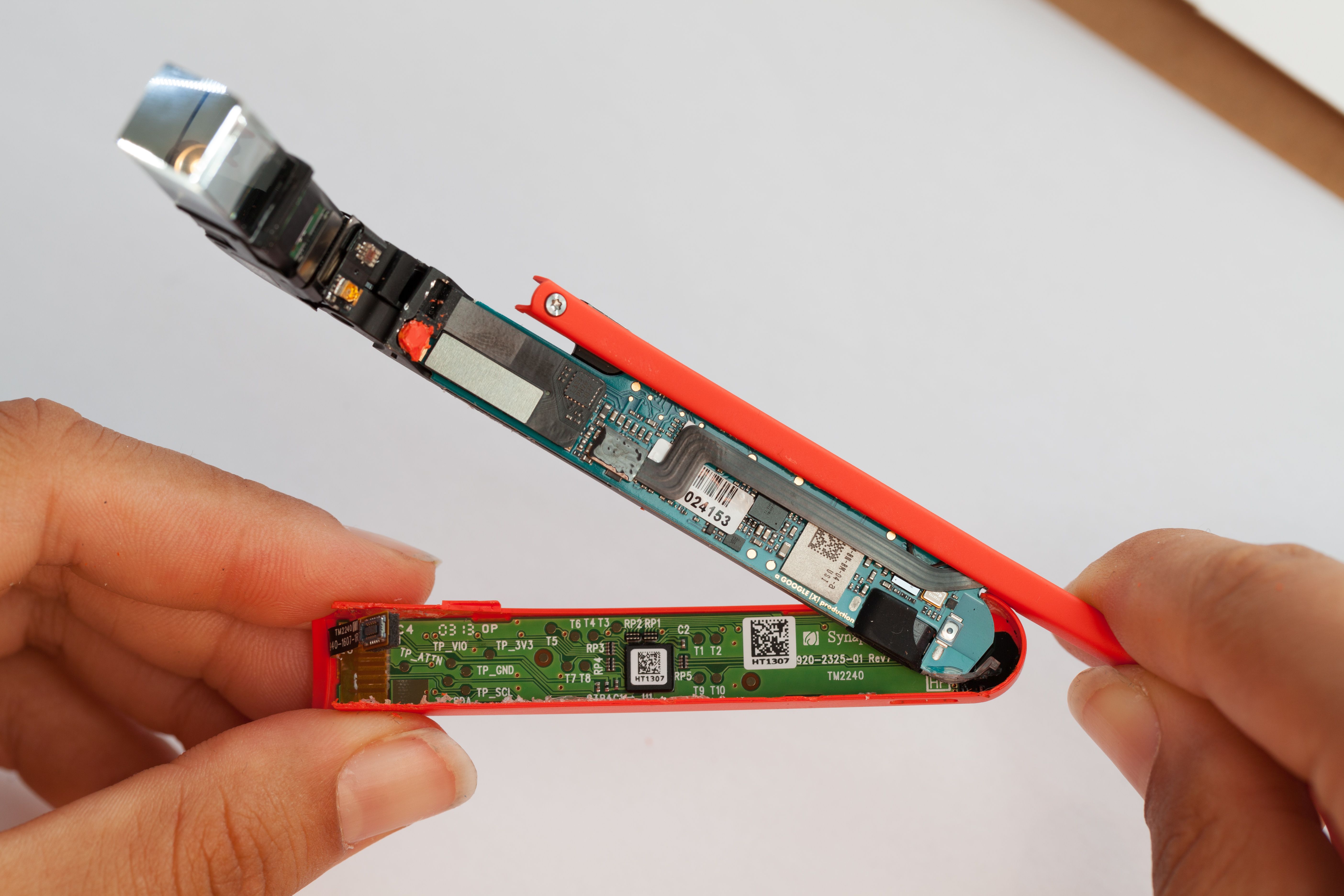
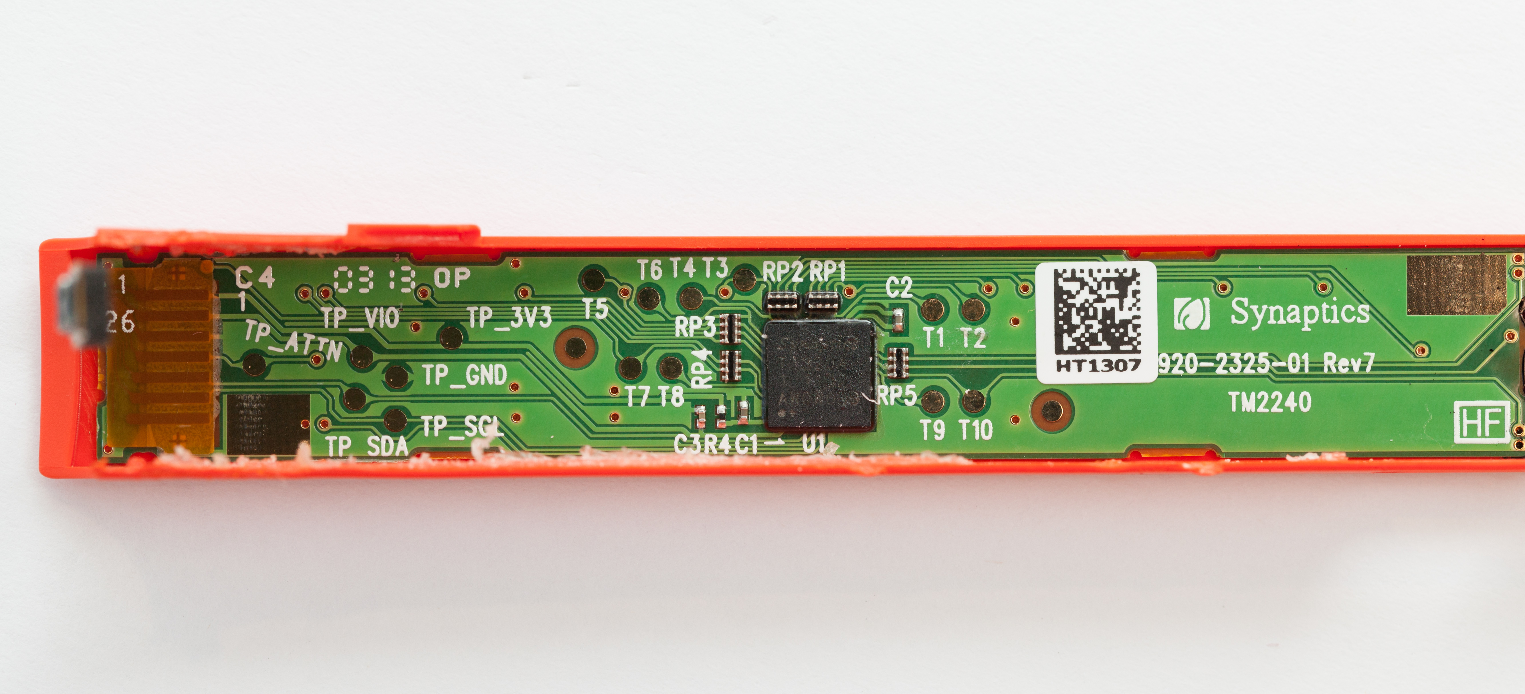
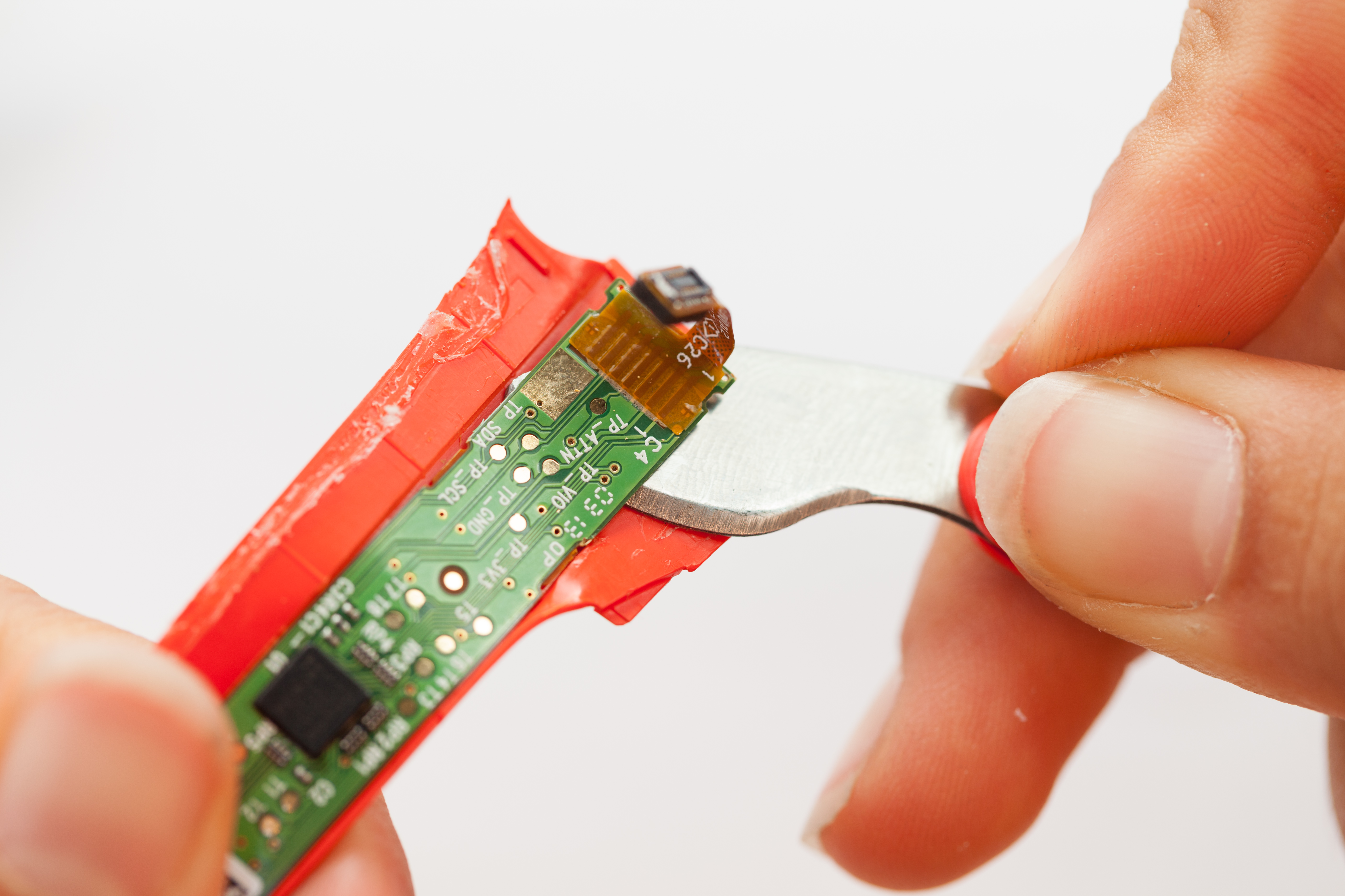
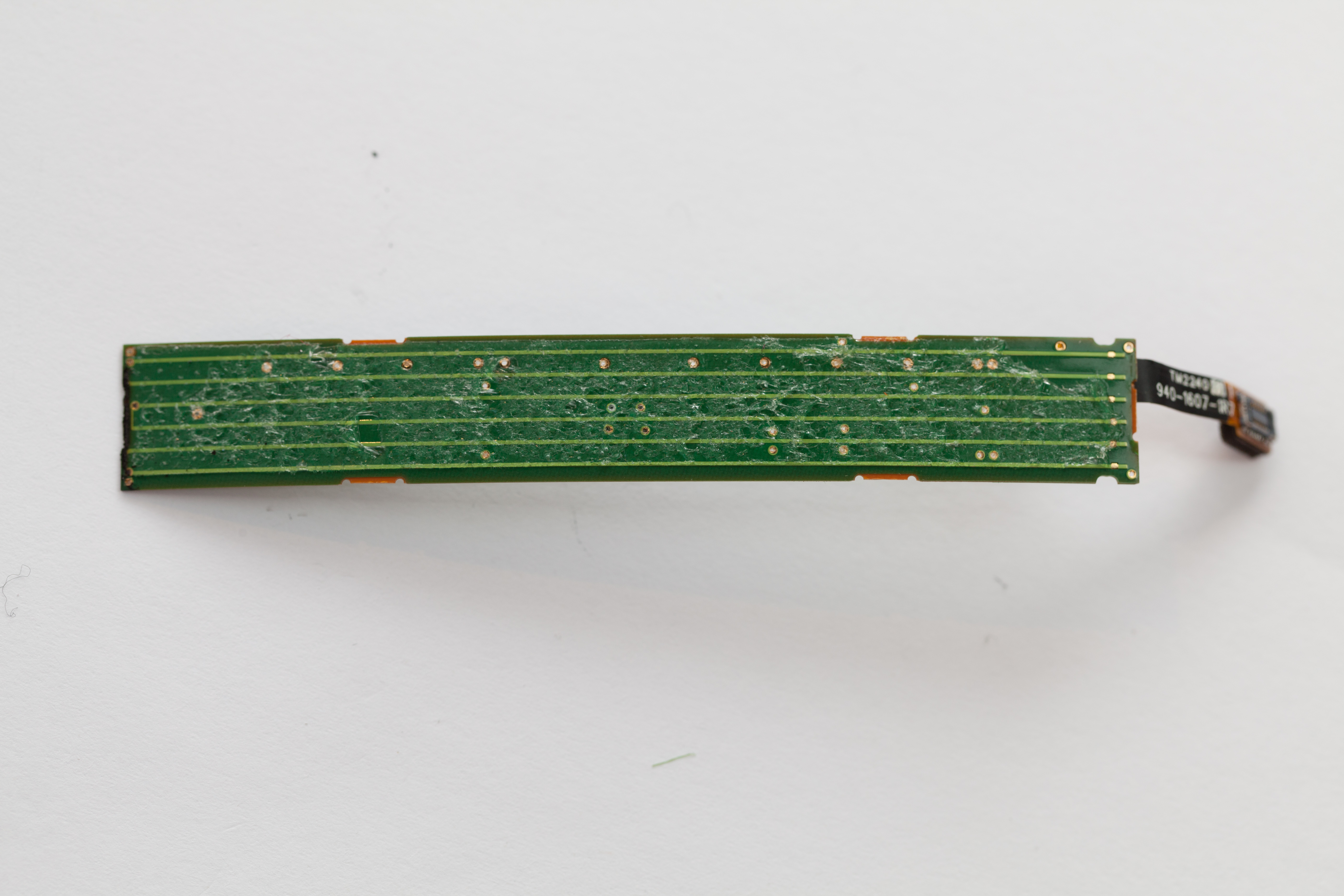
Removing the casing exposed a few parts, including the separate touchpad module on the right side of the unit. When a Glass users looks like they are pensively tapping their temple, they are interacting with this sensor. The touchpad is a full custom module made by Synaptics, and is driven by a Synaptics T1320A touchpad controller.
Main CPU Board
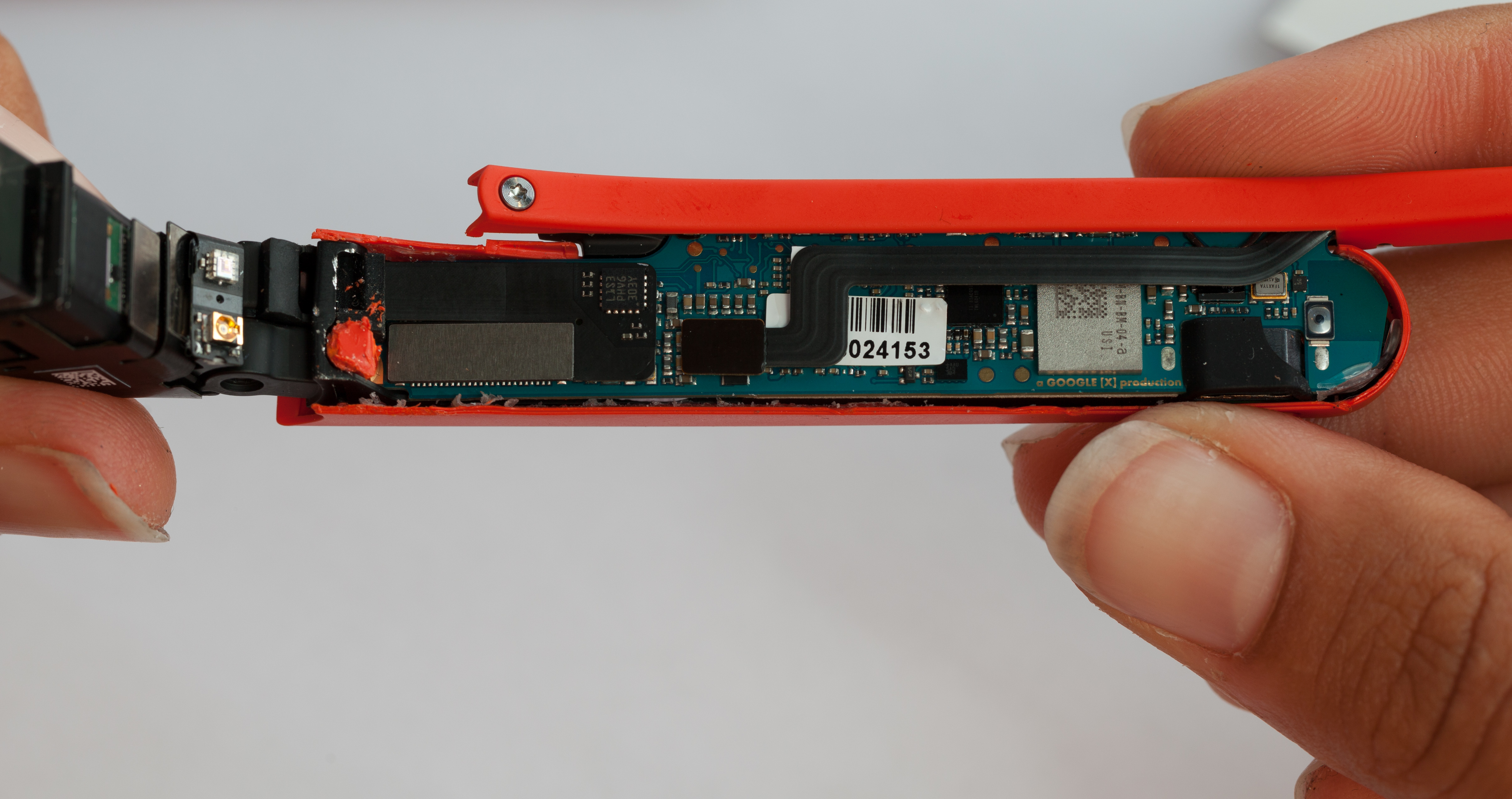
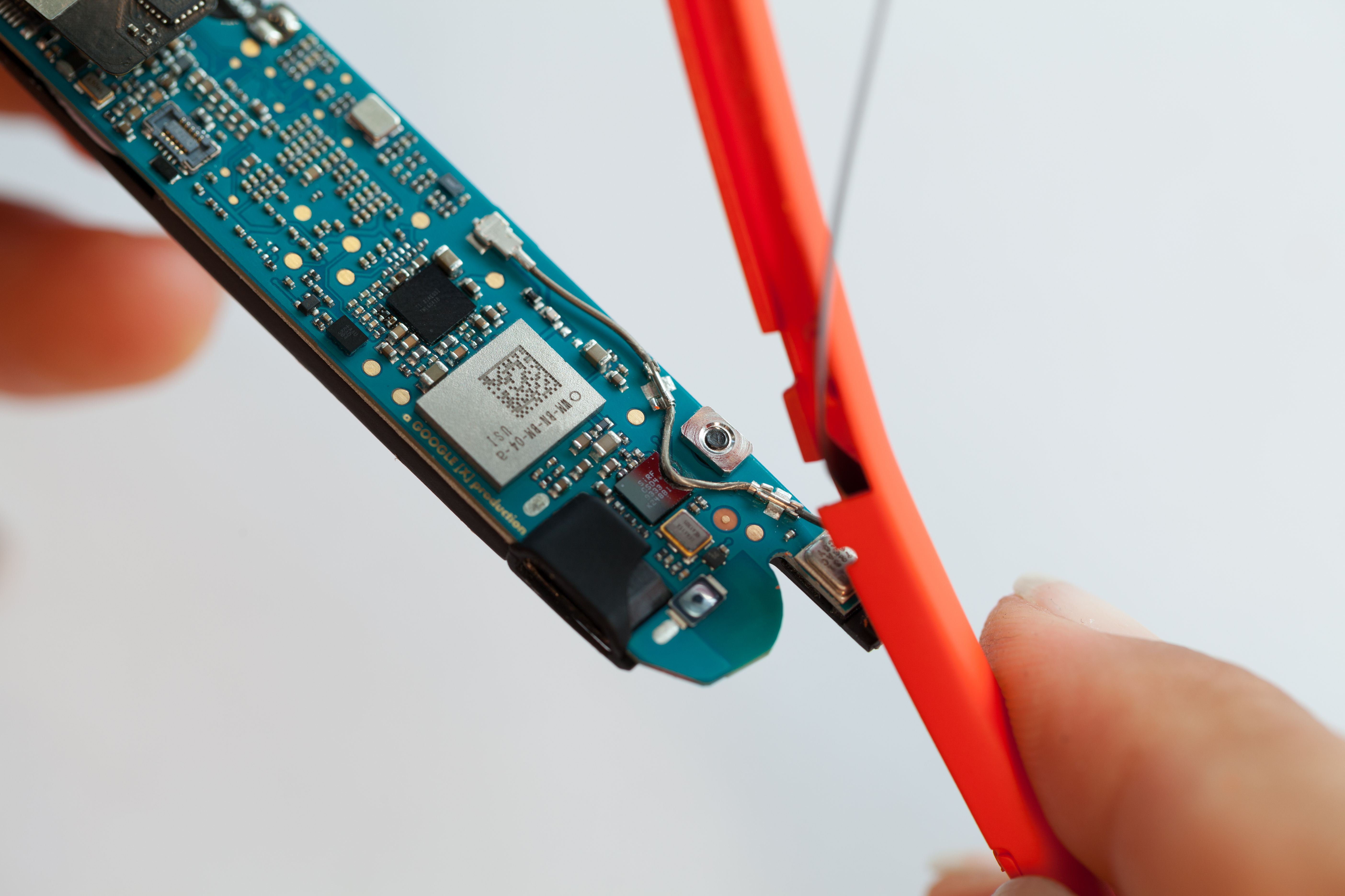
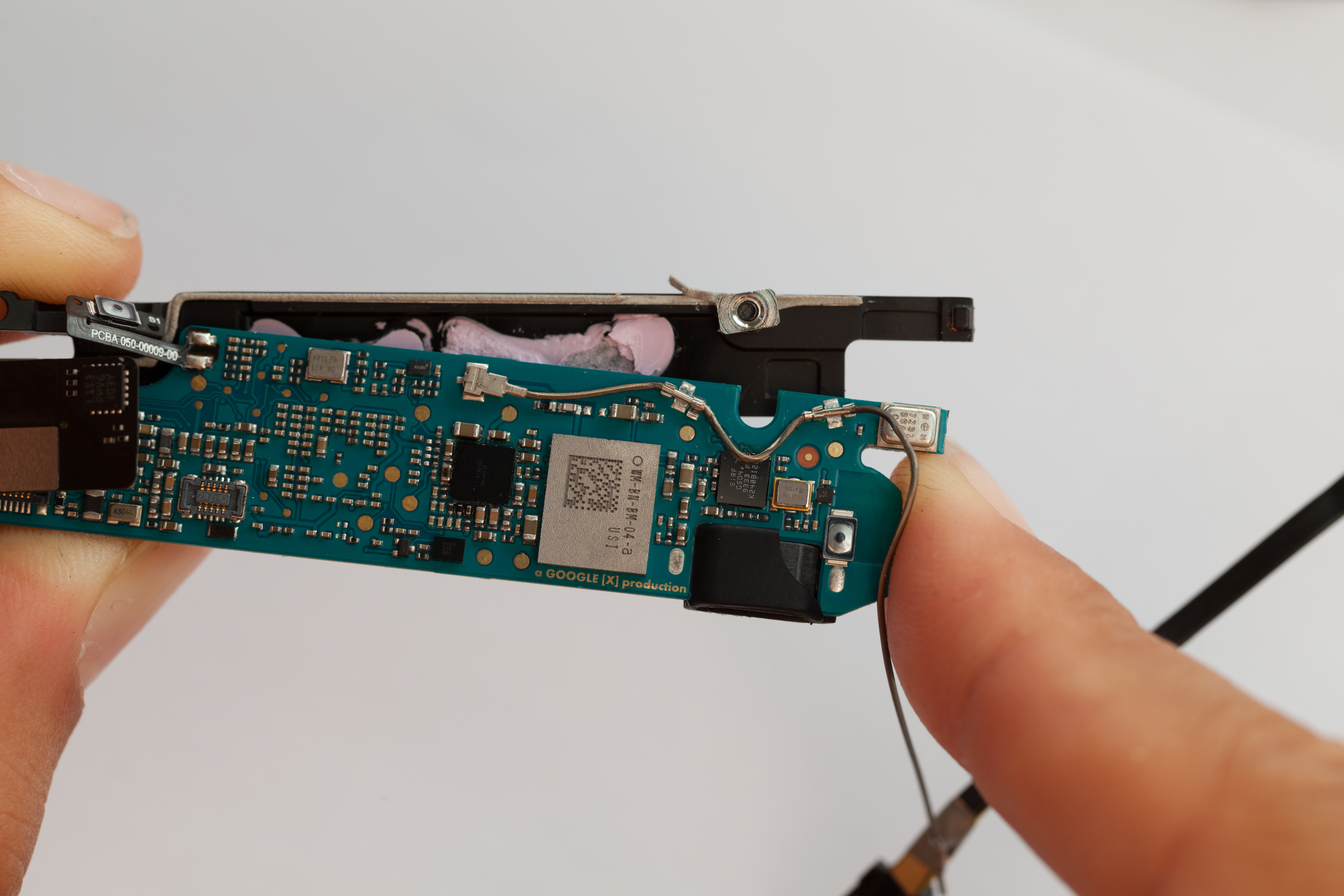
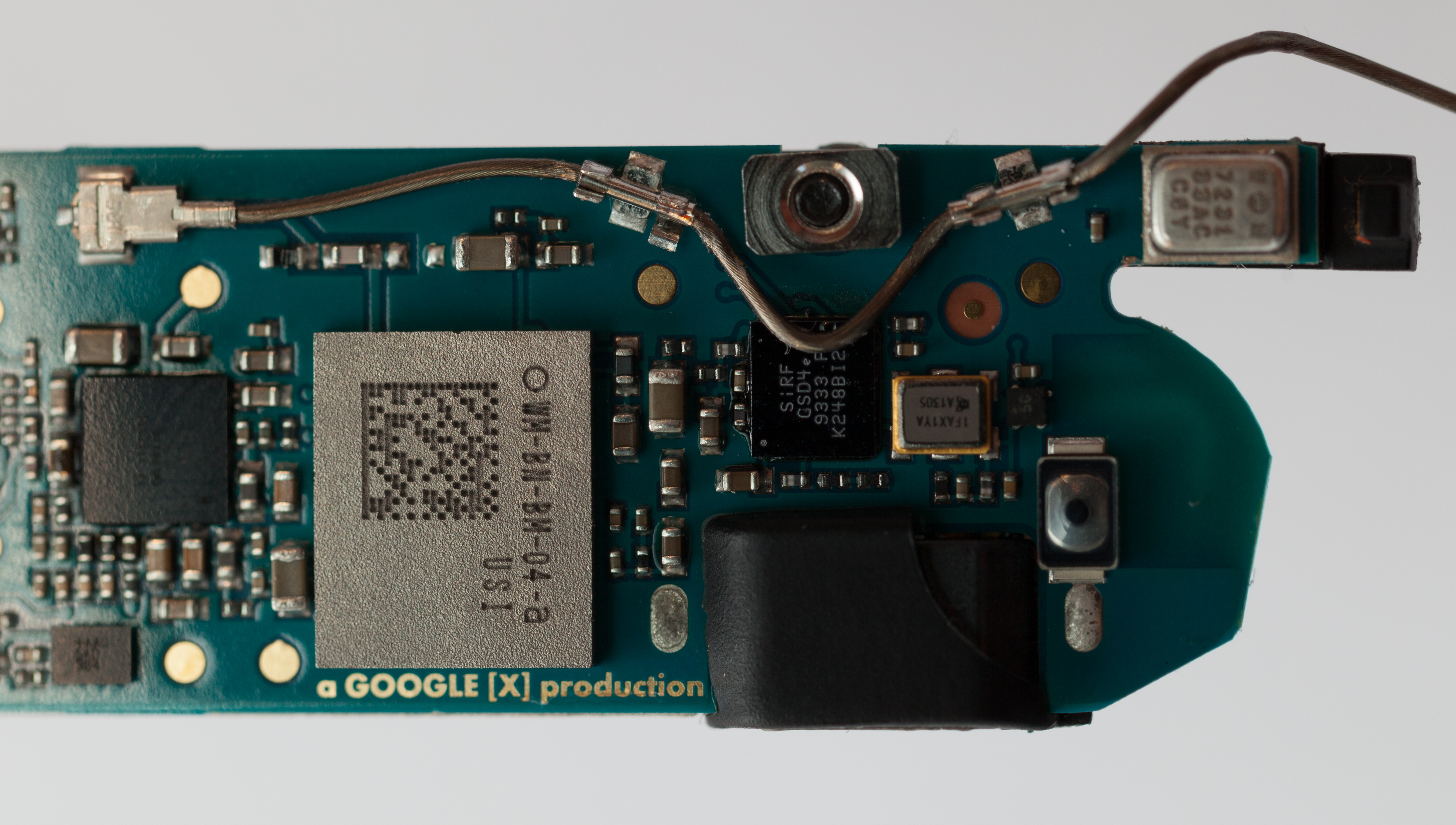
The main logic board was now exposed. The inwards-facing side holds an RF module, some small connectors and support ICs, and copper noting that this is "a GOOGLE [X] production".
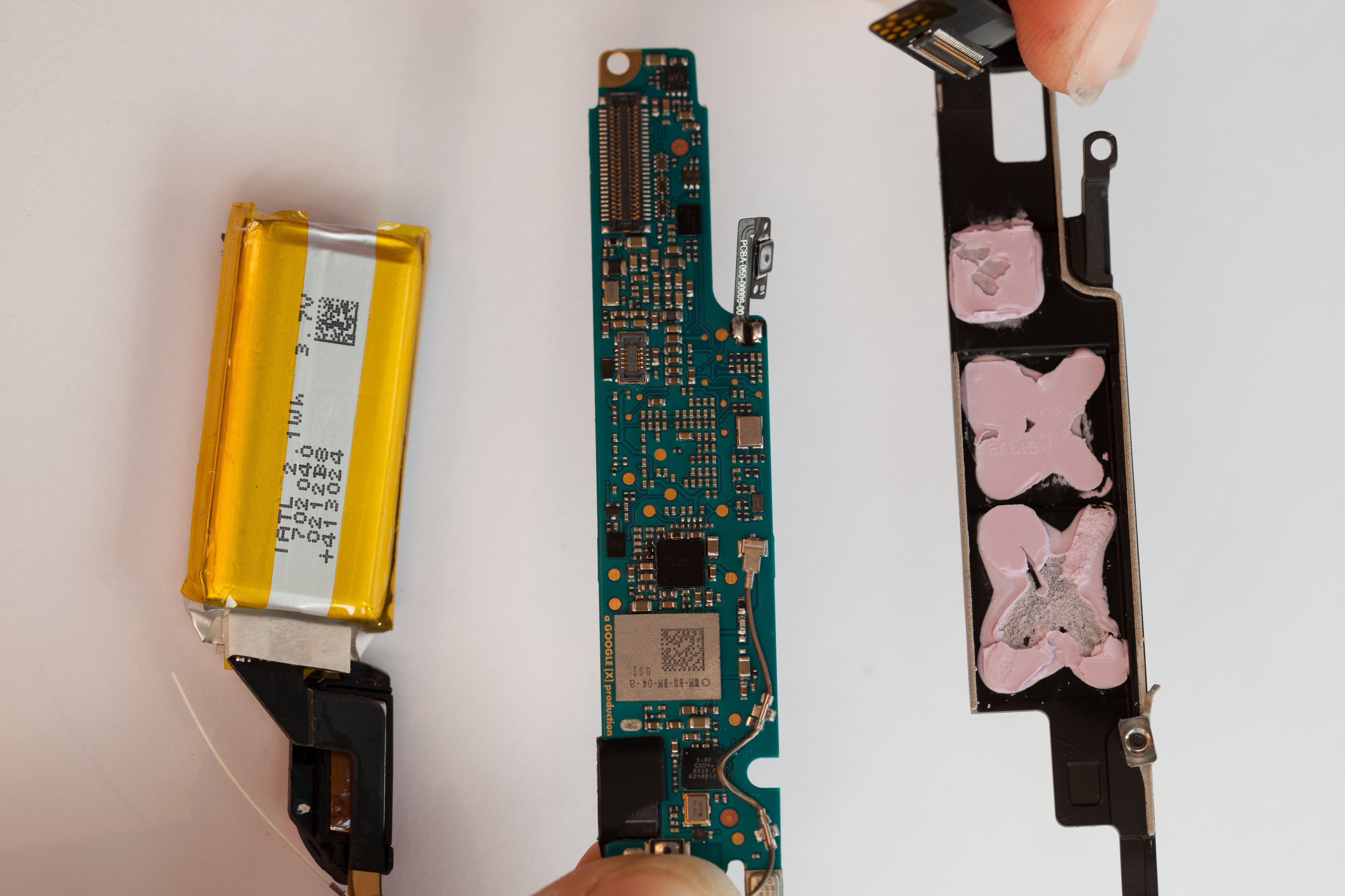
This board was stuck to a thermal pad with lots of paste. After removing it and cleaning off the pink thermal compound, we revealed the core chips powering Glass: a TI OMAP4430, 16GB of SanDisk flash, and an Elpida mobile DRAM chip. A flex PCB and an RF cable, anchored with some metal tabs and an MMCX (?) connector, trailed from this board to the behind-the-ear pod.
Some text in the copper on this board reads >9K!It's over 9000!
Behind-Ear Module
To keep the unit's weight distributed more evenly, Glass keeps its battery in a rounded bit behind the wearer's ear. We stripped this area open, again applying destructive force to tear the plastic.
The single-cell Lithium Polymer battery sits at the end of the flexprint PCB and is marked as having a capacity of 2.1 Wh (roughly 570 mAh). It is not user-replaceable, not even a little bit.
From Trend focus analysis of flash NAND Solid State Drive (SSD) market growth, prices by application and technology:
"MLC dominated the NAND market in CQ1 with 77.9% share, up 8% quarter on quarter.
TLC (3bit/cell) is gaining traction and rose 8% from quarter-to-quarter.
Samsung is the only company shipping TLC-based SSDs in volume.
SLC is declining quickly as demand transitions to MLC, except in certain high performance, high-endurance applications such as military, industrial, medical and automotive."
Leaders being in order Samsung, SanDisk, Toshiba and Intel
The NAND market continued to heat up, as NAND supply was tight in CQ1 '13 due to healthy demand and supply constraints. Nevertheless, the SSD market grew from the prior quarter to 13.28 million, up 22% quarter on quarter.
In CQ1, the client SSD market was up 19% sequentially to 12.06 million. Enterprise SSD growth rates continue to outpace any seasonal server or storage system softness - this market was up 66% from CQ4 '12, to 1.22 million.
Client SSDs were dominated by NAND suppliers, especially Samsung, who took the lead in selling TLC (3bit/cell) into PC OEMs and the retail channel. Toshiba and SanDisk, who had been the main drivers for TLC in the industry up to this point, could not sustain the momentum and lost share in the market.
The enterprise SSD market is gaining more traction in data centers and cloud storage, as the $/GB metric decreased to levels low enough to drive an inflection in demand. TCO and performance arguments are far more compelling at today's $/GB levels and with costs expected to continue downward, enterprise SSD adoption will continue to grow at rates outpacing other storage devices.
Total SSD Market by Application
Units in million
CQ1 '13 actuals
CQ1 '14 Forecast
Y/Y Growth
Client SSDs
Stand-Alone Units
7.073
10.180
44%
Cache Units
4.986
8.319
67%
Total
12.059
18.499
53%
Enterprise SSDs
SATA Units
1.009
1.151
14%
SAS Units
0.170
0.198
16%
PCIe Units
0.037
0.042
14%
Total
1.216
1.391
14%
Total SSD Units
13.275
19.890
50%
(Source: Trendfocus, May 2013)
Total NAND Market Share by Technology (Source: Trendfocus, May 2013)
Spot Market Pricing of SSDs (Source: Trendfocus, May 2013)
Price for SSDs in the spot market continues to rise due to constrained NAND supply. OEM and large-scale contracts can be markedly different than spot market pricing.
256GB SSD increased 57% from $145 in January to $227 in first week of May.
128GB SSD increased 87% since January to $140.
SSD Supplier Market Share in 1Q13
in million of units
Client
Enterprise
Total
Share
Samsung
4.092
0.060
4.152
31.3%
SanDisk
2.200
0.026
2.226
16.8%
Toshiba
1.222
0.000
1.222
9.2%
Intel
0.832
0.025
0.857
6.5%
HGST
0.000
0.094
0.094
0.7%
STEC
0.000
0.044
0.044
0.3%
Others
3.713
0.967
4.680
35.3%
Total
12.059
1.216
13.275
100%
(Source: Trendfocus, May 2013)
Our comments :
Now Trendfocus is becoming a serious analyst firm in SSDs after being concentrated for several years on HDDs disk heads and media only. Other ones in this flash sector include IDC and IHS iSuppli.
It's a difficult job because there are over 100 SSD makers around the world. It's easier to track HDDs with only three manufacturers remaining.
What is published above is a small abstract of the 29 pages of the Trenfocus report NAND/SSD Information Service - May 13, 2013, CQ1'13 Quarterly Update.
We just found the Californian analysts relatively conservative concerning the growth of the enterprise PCIe SSD market compared to the SAS one, and more globally on enterprise SSDs.



 Some highlights of teardown of google glass below.