Showing posts with label GPU. Show all posts

Wednesday, September 24, 2014

Apple's iPhone 6 A8 Teardown

Chipworks has been quick to teardown Apple's A8 processor, which is the secret sauce driving the new iPhone 6. Some details of the teardown are discussed below.

"Apple has spent quite a bit of die size on improving performance through more complex CPU and GPU architectures and miscellaneous feature additions."


A8 is fabricated on TSMC 20nm process while  A7 was manufactured on Samsung 28nm process. Shrinking the transistors gate to 20nm enables the CPU to operate faster. While limiting A8 to 4 GPU cores and not 6 help to reduce the new iPhone power.


Ron
Insightful, timely, and accurate semiconductor consulting.
Semiconductor information and news at - http://www.maltiel-consultin


Chipworks Disassembles Apple's A8 SoC: GX6450, 4MB L3 Cache & More

by Ryan Smith on September 23, 2014 1:00 PM EST

One of the more enjoyable rituals with Apple’s annual iPhone launch is the decapping, deconstruction, and photographing of the processor die at the heart of Apple’s newest SoC.  While we can learn a lot about the SoC from software, for some things there’s just no replacement for looking at the hardware itself and counting the functional blocks present. And this year, as in past years, the honor of being the first to tear apart the SoC goes to Chipworks.
For determining the layout of A8, Chipworks reached out to us to solicit our input on their die shot, and after some rounds of going back and forth we believe we’ve come to a solid determination of some of A8’s features and how it has been configured. So let's dive in.
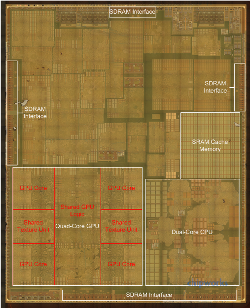
First and foremost we’ll start with A8’s GPU, as this was one of the hardest elements to analyze in software. Based on Apple’s 50% performance improvement we had previously speculated that A8 contained an Imagination PowerVR GX6650. However as we noted back then, a die shot would reveal all, and right on schedule it has.
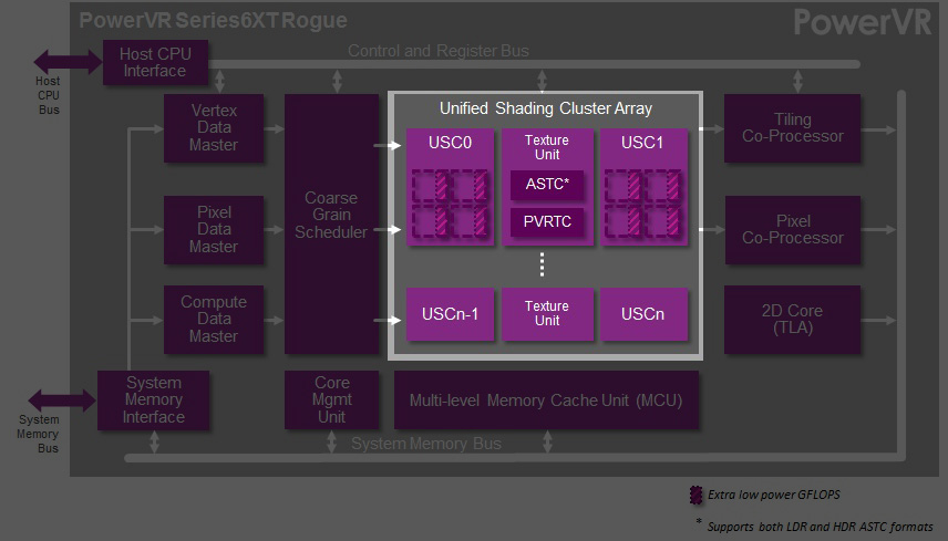
A close analysis of the die shot makes it clear that there are only 4 GPU cores available and not 6, which immediately rules out the 6 core GX6650 we were previously expecting. Instead with 4 cores present this is conclusive proof that Apple is using the smaller 4 core GX6450 on A8, the direct successor to the G6430 used on the A7. GX6450 induces some performance optimizations along with some feature updates – including ASTC support, which Apple’s documentation has already confirmed is present – so its inclusion here is a natural progression for Apple.
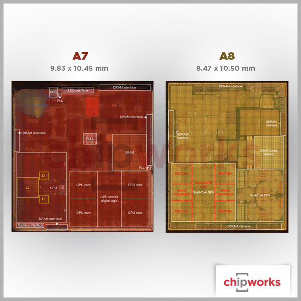
On A8 and its 20nm process this measures at 19.1mm2, versus A7’s 22.1mm2 G6430. As a result Apple is saving some die space compared to A7, but this is being partially offset by the greater complexity of GX6450 and possibly additional SRAM for larger caches on the GPU. Meanwhile looking at the symmetry of the block, it’s interesting that the blocks of texturing resources that every pair of GPU cores share is so visible and so large. With these resources being so big relative to the GPU cores themselves, you can see why Imagination would want to share them as opposed to building them 1:1 with the GPU cores.
Meanwhile opposite the GPU we have the CPU block. Unlike the GPU the CPU block has seen some significant shrinking, which Chipworks estimates is down from 17.1mm2 in A7 to 12.2mm2 in A8. In A7 Cyclone did not lend itself to easily picking apart the individual CPU cores, and neither does the CPU here in A8. We’ll be looking at the new CPU’s architecture in-depth in our iPhone 6 review, but for now it’s safe to say that while this is definitely derived from Cyclone, Apple has added a few tweaks over the last year that make it an even more potent CPU than the first Cyclone. Meanwhile based on this die shot Chipworks believes that the L2 cache has been reorganized to a per-core design, as there is no obvious single block of L2 on A8 like there was A7.
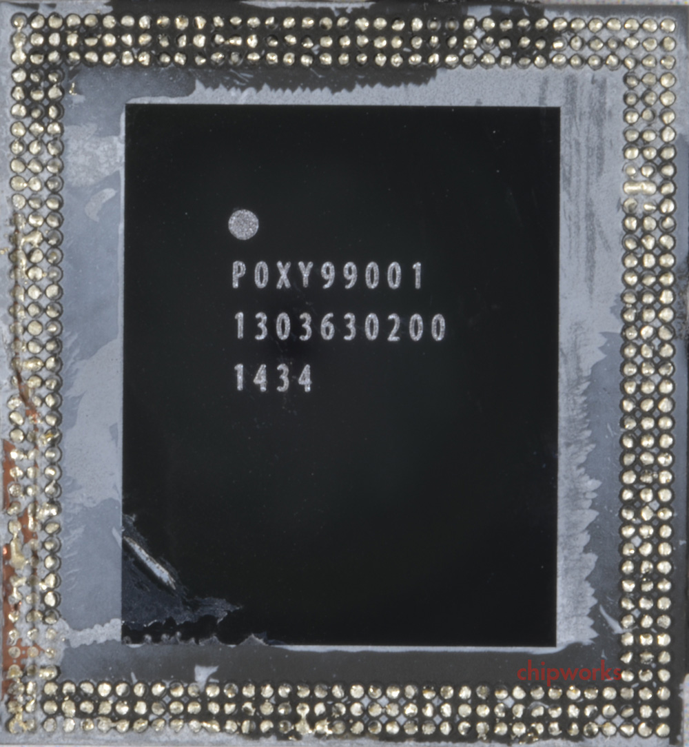
A8 With PoP DRAM Removed
The final major identifiable block on A8 is once again the SRAM cache memory. On A7 we discovered that this block was 4MB and was responsible for servicing the GPU and CPU. On A8 this block is similarly present and serving the same role. This 4MB of SRAM ends up being quite big despite the shrink from 28nm to 20nm, and while at first glance it seems like it should be larger than 4MB given the relative size, in practice what has happened is that the individual SRAM cells have not shrunk by a full 50%. Chipworks estimates the cell size to now be about 0.08µm2, versus 0.12µm2 on A7, which is closer to a 33% shrink that a 50% shrink. As a result the SRAM cache still takes up a fair bit of space, but the value of being able to serve larger memory requests without having to go off-die continues to be immense.
Apple A8 vs A7 SoCs
 Apple A8 (2014)Apple A7 (2013)
Manufacturing ProcessTSMC 20nm HKMGSamsung 28nm HKMG
Die Size89mm2104mm2
Transistor Count~2B"Over 1B"
CPU2 x Apple Enhanced Cyclone ARMv8 64-bit cores2 x Apple Cyclone ARMv8 64-bit cores
GPUIMG PowerVR GX6450IMG PowerVR G6430
Overall, Chipworks’ analysis points to A8 being fabbed on TSMC’s 20nm process. This makes A8 among the first SoCs to receive the 20nm treatment. Thanks to this smaller node Apple has been able to build in additional features to the SoC while simultaneously shaving off around 15% of their die size. Chipworks estimates the final die size of A8 to stand at 89mm2, versus the 104mm2 for the Samsung 28nm based A7. Chipworks notes that if this were a straight shrink that one would expect the A8 to be closer to 50% the size of A7 (though not all logic can shrink quite that well), which indicates that Apple has spent quite a bit of die size on improving performance through more complex CPU and GPU architectures and miscellaneous feature additions.
Wrapping things up, we’ll be back later this month with our review of the iPhone 6 family and our full analysis of the A8 SoC. So until then stay tuned.
Wednesday, May 9, 2012

Nvidia #1 at TSMC Fab? Nvida has Priority for 28nm capacity

"TSMC has given priority to Nvidia for 28nm capacity, according to industry sources" (see below).

Nvidia has been unsatisfied with TSMC's 28nm process
Photo: Monica Chen, Digitimes file photo


Complaining publicly did not hurt - see March 26, 2012 blog Nvidia: TSMC 20nm Essentially Worthless 


Ron


TSMC gives priority to Nvidia for 28nm capacity

http://www.digitimes.com/news/a20120509PD211.html?mod=2
Monica Chen, Taipei; Joseph Tsai, DIGITIMES [Wednesday 9 May 2012]

Taiwan Semiconductor Manufacturing Company (TSMC) has given priority to Nvidia for 28nm capacity, according to industry sources.
Since Nvidia has been unsatisfied with TSMC's 28nm process, while the company has also not refuted rumors that the company may cooperate with Samsung Electronics or Globalfoundries, TSMC, to sooth Nvidia, has put the GPU maker on its supply priority, allowing Nvidia to be able to release its 28nm GPUs on schedule in May and June.
The same situation has also happened previously with Qualcomm, which had said it would consider outsourcing orders to other wafer foundries, and successfully gained TSMC's promise for supply priority.
With both Qualcomm and Nvidia achieving supply priority from TSMC, players that are also waiting for TSMC's 28nm capacity, are expected to be affected.


Thursday, May 3, 2012

TSMC To Makes Processer Chip For Apple? Not so Quickly

DigiTime below states “Taiwan Semiconductor Manufacturing Company's (TSMC) plans to ramp up 20nm production ahead of schedule…to entice Apple”. TSCM already is having trouble processing enough 28nm wafers for their current customers, why would Apple want to give TSCM orders for the next generation 20nm process?

In addition, if we look at how Apple’s is handling the current A5 processor manufacturing. They currently use the 45nm process (New iPad-Teardown: Why Apple's A5X uses 45 nm). It indicates that Apple intentionally does not want to push the envelope of a new process technology at the same time that they are bringing up a new processor circuit. They prefers to use a more mature process while the pushing the limits on circuit design.

It is more likely that TSMC is more aggressive in developing the fab and the 20nm process just to enhance their market position relative to other foundry vendors for their current customers. See Nvidia: TSMC 20nm Essentially Worthless.
Another prespective is at TSMC has a “good chance” of winning Apple’s chip biz in 2014
Ron Maltiel


TSMC eyeing advanced process chip orders from Apple
Cage Chao, Taipei; Jessie Shen, DIGITIMES [Wednesday 2 May 2012]

Taiwan Semiconductor Manufacturing Company's (TSMC) plans to ramp up 20nm production ahead of schedule have prompted industry sources to speculate that the foundry will be aggressively striving for CPU orders for future Apple devices.

The present 28nm shortage at TSMC makes it more unlikely that the foundry could attract orders from Apple, the sources claimed. TSMC currently is unable to provide sufficient capacity to its existing 28nm customers, the sources said.

With orders placed by Qualcomm, Nvidia, Broadcom, TI and AMD, TSMC meets less than 70% of 28nm chip demand at present, the sources pointed out. While having tight supply of 28nm capacity, TSMC now hopes an early investment in 20nm technology will help the foundry engage in collaboration with potential clients such as Apple in advance and ensure enough capacity to meet demand, the sources indicated.

The sources added TSMC stands a good chance of landing CPU orders from Apple in 2014.

With regards to the speculation, Digitimes Research analyst Nobunaga Chai commented that the fundamental issue will still be whether Apple would use a 28nm or 20nm process to build its next-generation processor, and choose TSMC as its contract manufacturer. If TSMC succeeds in grabbing CPU orders from Apple, the foundry's supply capability should not be a problem at all, Chai said.

Apple still uses 45nm to make its newest A5X, and has Samsung Electronics build the chips.

TSMC has revealed plans to invest about US$700 million in building a 20nm R&D line in 2012 – instead of its originally-planned 2013. Acknowledging that demand for 28nm manufacturing capacity from its mobile product IC customers has been higher than expected since the process ramp-up, the foundry finds it necessary to put its 20nm process into production ahead of schedule. Demand for 20nm will also first come from the mobile device sector, and order volumes are likely to be huge during the initial ramp-up stage – similar to the situation 28nm has, TSMC said at its recent investors meeting.

TSMC also indicated that the firm has accelerated its pace of 28nm capacity expansion. The foundry expects to have its supply of 28nm chips close to catching up with demand in the fourth quarter of 2012, and satisfy demand completely by the first quarter of 2013.


Monday, March 26, 2012

Nvidia: TSMC 20nm Essentially Worthless

TSMC is having problems with 20nm process, while Intel and Samsung don't appear to have these problems.  Is running their own fabs giving Intel and Samsung key yield and cost benefits?


Ron Maltiel


Nvidia deeply unhappy with TSMC, claims 20nm essentially worthless

http://www.extremetech.com/computing/123529-nvidia-deeply-unhappy-with-tsmc-claims-22nm-essentially-worthless
By Joel Hruska on March 23, 2012
 
One of the unspoken rules of customer-foundry relations is that you virtually never see the former speak poorly of the latter. Only when things have seriously hit the fan do partners like AMD or Nvidia admit to manufacturing problems, and typically only after postponed launches and poor availability have made protestations that everything is fine unsustainable.


That’s why we were surprised — and our source testified to being stunned — that Nvidia gave the following presentation at the International Trade Partner Conference (ITPC) forum last November. Many of the company’s complaints regarding its current partnership with TSMC are exactly what you’d expect given the manufacturing problems the entire industry is facing. What’s surprising are Nvidia’s remarks concerning TSMC’s current cost curves and manufacturing ramps. This is normally the sort of information discussed quietly between a foundry and its customers or by the press with help from various anonymous sources. Discussing the problems publicly is a sign of just how frustrated the company has become.


Watch the underlines for emphasis

TSMC builds hardware for a huge number of companies, but those customers have very different needs and use a wide range of process technologies. Historically, Nvidia (and ATI/AMD) have been regular early adopters. The nature of graphics is that it can easily soak up new processes and the higher transistor counts they enable.


Kepler broke the exponential rise in transistors per GPU

The flip side of that situation is that companies like AMD and Nvidia have also been responsible for assuming the risks associated with “risk production” and footing a hefty bill for the privilege. As those risks mount and costs skyrocket, Nvidia is increasingly unhappy with being asked to shoulder the burden. Nvidia’s slides talk about the need for “real” understanding, compromises on “rough justice,” and a closer relationship that looks more like that of an IDM (Integrated Device Manufacturer). For those of you who don’t know the term, Intel is an IDM — it handles both manufacturing and design. AMD used to be.

When AMD spun GlobalFoundries off, one of the things GF promised to provide that would distinguish it from TSMC was high levels of IDM-style integration. At TSMC, the customization work that is available is highly monetized; specialized work is expensive and time-consuming. In reality, GF’s ability to provide the amount of IDM-like flexibility that it wanted to offer has been sharply constrained by the problems associated with Llano and Bulldozer; our sources tell us that the foundry devoted enormous resources to bringing AMD’s 32nm APU back on track.

According to Nvidia, the current model is unsustainable. Here’s the company’s projected analysis for transistor costs at current and new nodes.


As the process nodes shrink, it takes longer and longer for the cost-per-transistor to fall below the previous generation. At 20nm, the gains all-but vanish. Want to know why Nvidia rearchitected Fermi with a new emphasis on efficiency and performance/watt? You’re looking at the reason. If per-transistor costs remain constant, the only way to improve your cost structure is to make better use of the transistors you’ve got.

As for wafer costs, they’ve become part of the problem.


What this slide states — we can’t even call it a suggestion — is that smaller processes no longer improve yields by leading to a greater number of chips per wafer. Instead, the complexities and difficulties of manufacturing at the new process create a cost structure that provides precious little incentive to manufacture at the new process.

If openly criticizing a foundry partner is unusual, showing data that suggests that your foundry partner can’t provide a cost-effective strategy for building hardware at next-generation process nodes is… a few steps past that point. The recent launch of the GTX 680, and that card’s trifecta of price/performance/power-efficiency actually strengthens the impact of this data. NV would’ve had a good idea how the GK104 was shaping up when it spoke at ITPC in November; this isn’t a case where a company is angry about the performance of a particular part and looking for someone to blame.

Again, follow the underlines.

The GK104 is great, but it doesn’t change the nature or severity of the underlying problems. As for whether Nvidia’s unhappiness with TSMC heralds a potential alliance with GlobalFoundries, we’re dubious. Not only has GF only recently ironed out its own 28nm issues, the nature of the foundry business doesn’t allow for quick shifts. Indeed, part of the reason that manufacturers like TSMC have historically exercised such control over their partners’ PR releases is because once you’ve committed to a foundry, you’re locked in for a substantial period of time. The fact that there’s now two foundries available with cutting-edge technology doesn’t change that, and the Common Platform Alliance favored by IBM, Samsung, and GloFo only mitigates some of the problems with moving a design from foundry to foundry, it doesn’t remove them.

The real question, at least for TSMC’s other customers, is whether the graphs and charts Nvidia has shown are specific to the company’s own products or reflect universal trends. There’s good reason to suspect the latter; Nvidia may have had more trouble than some of TSMC’s other customers, but our analysis of semiconductor industry roadmaps revealed a great deal of uncertainty about the road forward. Nvidia opted to aggressively optimize GK104 precisely because the old strategy of bolting on more cores and ratcheting up transistor counts isn’t sustainable.

Further evidence for the accuracy of NV’s presentation comes, ironically, from the company’s primary GPU competitor. At AMD’s Financial Analyst Day, CEO Rory Read made a point of saying that the company no longer intends to aggressively transition to new process nodes given the diminishing marginal returns from doing so.

Change the color scheme, and Nvidia’s graphs could’ve dropped right into AMD’s presentations in early February.

Nvidia’s willingness to stand up and talk about these problems is an “Emperor’s new clothes” sort of moment. The long-term repercussions, if any, are still unclear.