Showing posts with label SoC. Show all posts

Wednesday, September 21, 2016

Manufacturing cost of iPhone 7

IHS published a "bill of materials (BOM) for an iPhone 7 equipped with 32 gigabytes (GB) of NAND flash memory carries $219.80 in bill of materials costs". See more in the article below.

Apple A10 Fusion APL1W24 SoC + Samsung 3 GB LPDDR4 RAM (from https://www.ifixit.com/Teardown/iPhone+7+Plus+Teardown/67384)
Some of the high cost chips used in the iPhone will go down in price; for example the System-on-Chip (SOC) at a cost of $26.90 (made by TSMC) and the NAND memory chips (made by Hynix) and SDRAM (made by Samsung) at a combined cost of $16.40. The price of the iPhone 7 will not go down.


Ron
Insightful, timely, and accurate semiconductor consulting.
Semiconductor information and news at - http://www.maltiel-consulting.com/


The iPhone 7 costs Apple more than you think


LONDON--()--The bill of materials (BOM) for an iPhone 7 equipped with 32 gigabytes (GB) of NAND flash memory carries $219.80 in bill of materials costs, according to a preliminary estimate from IHS Markit (Nasdaq: INFO), a world leader in critical information, analytics and solutions.
“Total BOM costs for the iPhone 7 are more in line with what we have seen in teardowns of recent flagship phones from Apple’s main competitor, Samsung, in that the costs are higher than in previous iPhone teardown analyses,” said Andrew Rassweiler, senior director of cost benchmarking services for IHS Markit. “All other things being equal, Apple still makes more margin from hardware than Samsung, but materials costs are higher than in the past.”After $5 in basic manufacturing costs are added, Apple’s total cost to manufacture the iPhone 7 rises to $224.80. The unsubsidized price for a 32GB iPhone 7 is $649. IHS Markit has not yet performed a teardown analysis on the larger iPhone 7 Plus. This preliminary estimated total is $36.89 higher than the final analysis of the iPhone 6S published by IHS in December 2015.

Apple iPhone 7 32GB (A1778) 
   Cost Summary  
Direct Material Costs $219.80
(Component Costs)
Conversion Costs$5.00
(Assembly / Insertion / Test Costs)
Total Cost$         224.80         
(Direct materials and manufacturing)
         
Itemized Components Manufacturer Name          Manufacturer Part Number Description Total Cost
Apps Processor        
System-on-Chip TSMC (Apple) APLW24 
Apple A10, Quad-Core 64-Bit ARM Based CPU, Hexa-Core
GPU, 16nm FinFET
 $         26.90
Baseband / RF / PA                $         33.90
Baseband INTEL CORP PMB9943 Baseband Processor, Multi-Mode  
RF Transceiver INTEL CORP PMB5750 RF Transceiver, Multi-Mode (Qty:2)  
RF Front End        
Antenna Switch Module TDK CORP D5313 Antenna Switch Module, w/ Filters  
Antenna Switch Module TDK CORP D5325 Antenna Switch Module, w/ Filters  
Envelope Tracking QORVO INC 81003M Envelope Tracking IC  
FEM BROADCOM LTD (AVAGO) DFI620 FEM  
FEM SKYWORKS SKY13702-20 FEM  
FEM SKYWORKS SKY13703-21 FEM  
PAM BROADCOM LTD (AVAGO) AFEM-8050 PAM  
PAM BROADCOM LTD (AVAGO) AFEM-8060 PAM  
PAM QORVO INC RF6110 PAM  
PAM SKYWORKS SKY77359 PAM  
Battery        
  HUIZHOU DESAY   Li-Polymer, 3.8V, 1960mAh $         2.50
         
BT / GNSS / WLAN       $         8.00
BT / WLAN 
UNIVERSAL SCIENTIFIC INDUSTRIAL
 S39S00201 BT / WLAN Module  
GNSS BROADCOM LTD BCM47734IUBG GNSS Receiver  
Front End     BT / WLAN & GNSS Front End  
Cameras       $         19.90
Front FaceTime     7MP BSI w/ Fixed Lens  
Rear     12MP BSI, w/ AutoFocus, & Optical Image Stabilization  
Display       $         43.00
Display / Touchscreen Module     4.7" 1334x750 LTPS IPS LCD, w/ In-Cell Touch  
Electromechanicals                $         16.70
Taptic Engine     Taptic Engine  
Other Electro-MechanicalsAntennas, Connectors, Microphones, PCBs, Speakers, etc.
          
Glue Logic       $         1.30
  LATTICE SEMICONDUCTOR ICE5LP4K-SWG36I          FPGA - iCE40 Ultra, 40nm  
Mechanicals       $         18.20
Enclosure     Enclosure, Main, Bottom - Machined Aluminum  
Other Mechanicals     Hardware, Labels, Insulators, Shielding, vents, etc.  
Memory       $         16.40
NAND SK HYNIX H23QEG8VG2ACS-BC 32GB NAND  
SDRAM SAMSUNG SEMICONDUCTOR K3RG1G10CM-YGCH 2GB LPDDR4 PoP  
Power Management       $         7.20
PMIC - Main DIALOG SEMICONDUCTOR 338S00225 PMIC - Main  
PMIC - RF INTEL PMB6826 PMIC - RF  
Others     Other PMICs, Transistors, Diodes, etc.  
User Interface       $         14.00
Audio codec CIRRUS LOGIC CS42L71 Audio Codec  
Audio Amplifier CIRRUS LOGIC 338S00220 Audio Amplifier (Qty:3)  
NFC NXP PN67V NFC Controller  
Others     Interface Ics, discretes, passives, etc.  
Sensors        
Barometer BOSCH SENSORTEC GMBH            Barometric Pressure Sensor  
e-compass ALPS   Electronic Compass  
Other Sensors     
Accelerometer, Gyroscope, Touch ID Fingerprint
sensor, ALS/Proximity sensor, etc.
 
         
Box Contents       $         11.80
Lightning Cable     USB to Lightning  
Lightning to 3.5mm Audio Adapter     Audio Adapter, Lightning to 3.5mm Jack  
Headset w/ Lightning Connector              Headset, Stereo, w/ Lightning Connector  
Charger

Same shape. No jack.
While the overall shape and physical design of the iPhone 7 is similar to the iPhone 6S that preceded it, the new display has wider color gamut, including DCI-P3 as well as traditional sRGB, which improves the rendering of photos and videos. The device’s haptic engine, which provides the “click” feel for users, has also been improved for longer-duty cycles and better dynamic response. The home button is now static and mimics the MacBook in terms of a solid-state button design.
Apple has also eliminated the 3.5 millimeter headphone jack, allowing a larger battery and haptic motor. “Where there was an audio jack in the previous design, Apple replaced it with a symmetrical grill -- not for speakers, but for the waterproof microphone, leaving more room for the larger battery and Taptic Engine,” Rassweiler said.
Increased base-model storage
Apple has increased the iPhone 7’s storage density. For the first time, the base model starts at 32 gigabytes (GB) – which is only the second time Apple has upgraded the base storage in the iPhone. From a cost perspective, the shift from 16GB/64GB/128GB iPhones to 32GB/128GB/256GB is a big jump. “Despite significant cost erosion in NAND flash over the last year, this increase in the overall memory cost definitely puts pressure on the bill of materials costs -- and therefore margins -- from Apple’s perspective,” Rassweiler said.
Intel returns
The Intel design win, and six years of absence that Intel had from the iPhone, is important to note. Even so, Intel still shares the processor business with Qualcomm. “Whereas Apple strives to have ‘one iPhone model for all carriers and markets,’ there are a number of different hardware permutations supporting various countries and carriers,” Rassweiler said. “Apple will likely look for ways to simplify the design moving forward, which means one supplier – whether Intel or Qualcomm – will likely dominate, as part of supplier and SKU streamlining.”
According to Wayne Lam, principal analyst of smartphone electronics, IHS Markit, “Largely left behind in the 4G LTE market, Intel has finally worked itself back into the iPhone, which is a huge win, but not one that is going to be financially significant in the near term for Intel.”
RF paths
Apple has also eliminated segmented antenna bands, which means the company is pushing all radio-frequency (RF) paths to the very ends of the phone – both on the top and bottom. The aluminum uni-body construction and design forces all RF paths into those two locations. Whereas other smartphones use a glass back and RF components with antennas mounted on the ample back spaces, Apple is restricted to just two physical antennas. “This design limitation may force Apple to go back to an all-glass design again so that they can fit in 4x4MIMO LTE antennas and more features like wireless charging in the next iPhone iteration,” Lam said.
Modem moved
The baseband thin modem has been moved next to the A10 processor. Prior to the iPhone 7, the thin modem was always on the other side of the SIM card receptacle. “This is a subtle change but likely shows us where Apple wants to take this,” Lam said, “eventually putting the thin modem right on the apps processor package or even integrating it into the A-series processor.”
Officially water resistant
iPhone 7 is now officially rated as water resistant. “We also saw evidence of this water proofing design evolution in the earlier iPhone 6S, which included additional gasketing around critical connectors, as well as the use of WiFi antenna at the end of the primary speaker box,”Lam said. “Doing so pushes the antennas near the only other opening, for better reception and transmission.”
Jet-black polished case
Jet black polish is a new option on 128GB and 256GB models. “This is a new feature that produces a whole new look for the iPhone,” Lam said. “It is a lower yielding, time-intensive manufacturing step that adds cost, as well as considerable value, pushing the retail price higher for those requesting this option.”
Antenna speaker design
The antenna speaker design on the iPhone 7 came from the WiFi antenna packed into the speakers of Apple’s MacBook. “Apple likes to reuse these unique designs throughout their product lines,” Lam said. In a first for the iPhone series, the headset speaker now doubles as a stereo speaker.
Upgraded camera
While not as groundbreaking as the two optical paths in the iPhone 7 Plus, the iPhone 7 camera has now been upgraded to optical image stabilization (OIS), for better low light performance.
Improved battery life
The battery has been increased to 1960mAhr capacity from 1715mAh in the previous iPhone 6s. This change is consistent with Apple’s claims of improved battery life.

IHS Markit (www.ihsmarkit.com)
IHS Markit (Nasdaq: INFO) is a world leader in critical information, analytics and expertise to forge solutions for the major industries and markets that drive economies worldwide. The company delivers next-generation information, analytics and solutions to customers in business, finance and government, improving their operational efficiency and providing deep insights that lead to well-informed, confident decisions. IHS Markit has more than 50,000 key business and government customers, including 85 percent of the Fortune Global 500 and the world’s leading financial institutions. Headquartered in London, IHS Markit is committed to sustainable, profitable growth.
IHS Markit is a registered trademark of IHS Markit Ltd. All other company and product names may be trademarks of their respective owners © 2016 IHS Markit Ltd. All rights reserved.

Contacts

IHS Markit
Lee Graham, +1 303-397-2468

Tuesday, September 29, 2015

Surprise, Samsung's A9 Processor is 9% Smaller than TSMC''s in iPhone 6s


Chipworks reversed engineered Samsung's and TSMC's A9
Apple is using both Samsung and TSMC to fabricate the microprocessor for the new iPhone 6 and 6s (see the article below). A second source is typically used to cut down the risk of depending on only one fab for key component.  It is very interesting that the die size of Samsung is 96 mm2 while TSMC die size is 8.85% larger at 104.5 mm2.

Apple improved the approach of using a second source. It implemented two versions at the same time. When you develop new complex products such as A9 with an embedding mobile processor inside A9 , there are risks that the new processor would not work. By using one design at TSMC, and a shrunk version at Samsung, Apple got ahead on the learning curve. It gave Apple a chance to implement improvement while shrinking the die. In addition, the shrunk die at Samsung reduces the cost of the A9 die.

It will be interesting to know if there are some performance differences between Samsung and TSMC versions.


Ron
Insightful, timely, and accurate semiconductor consulting.
Semiconductor information and news at - http://www.maltiel-consulting.com/


Chipworks: Both Samsung and TSMC are making the A9 chip for Apple

And the Samsung version is smaller than the TSMC version.


The only thing that most people will need to know about Apple's A9 is that it's a whole lot faster than last year's A8. But for those of you who are more interested in chip design, Chipworks has unearthed an interesting tidbit: there are two different versions of the A9 chip, one manufactured by Samsung and another by Taiwan Semiconductor (TSMC). Most interestingly, Samsung's version (the APL0898) has a slightly smaller footprint than the TSMC version (APL1022).
There have long been rumors that Apple was dual-sourcing the A8 from Samsung and TSMC, but this is the first visual proof that we've seen of the practice. iPhone and iPad processors up to and including the A7 were all made by Samsung.
Apple buys other parts from multiple sources including NAND flash and RAM, but the SoC is a major component with bigger implications for performance and power. Chipworks promises a more in-depth look at how the two processors are different, but for now, all we know is that they differ in size.
We have no way to confirm whether the chips in our review samples were made by Samsung or TSMC. iFixit's teardowns found the Samsung version of the A9 in the iPhone 6S and TSMC's version in the iPhone 6S Plus, which makes sense—a larger phone has more room to spare for a larger chip—but that doesn't necessarily mean that all of the phones are being put together this way. In our testing, both the iPhone 6S and 6S Plus benchmarked nearly identically, and both behaved well during Geekbench's thermal throttling test.

Wednesday, September 24, 2014

Apple's iPhone 6 A8 Teardown

Chipworks has been quick to teardown Apple's A8 processor, which is the secret sauce driving the new iPhone 6. Some details of the teardown are discussed below.

"Apple has spent quite a bit of die size on improving performance through more complex CPU and GPU architectures and miscellaneous feature additions."


A8 is fabricated on TSMC 20nm process while  A7 was manufactured on Samsung 28nm process. Shrinking the transistors gate to 20nm enables the CPU to operate faster. While limiting A8 to 4 GPU cores and not 6 help to reduce the new iPhone power.


Ron
Insightful, timely, and accurate semiconductor consulting.
Semiconductor information and news at - http://www.maltiel-consultin


Chipworks Disassembles Apple's A8 SoC: GX6450, 4MB L3 Cache & More

by Ryan Smith on September 23, 2014 1:00 PM EST

One of the more enjoyable rituals with Apple’s annual iPhone launch is the decapping, deconstruction, and photographing of the processor die at the heart of Apple’s newest SoC.  While we can learn a lot about the SoC from software, for some things there’s just no replacement for looking at the hardware itself and counting the functional blocks present. And this year, as in past years, the honor of being the first to tear apart the SoC goes to Chipworks.
For determining the layout of A8, Chipworks reached out to us to solicit our input on their die shot, and after some rounds of going back and forth we believe we’ve come to a solid determination of some of A8’s features and how it has been configured. So let's dive in.
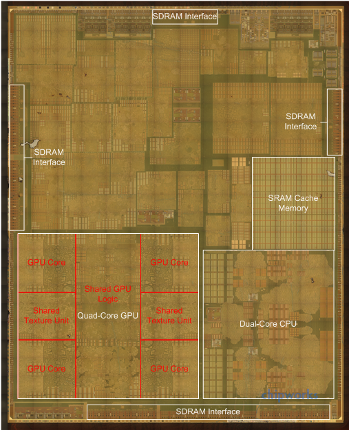
First and foremost we’ll start with A8’s GPU, as this was one of the hardest elements to analyze in software. Based on Apple’s 50% performance improvement we had previously speculated that A8 contained an Imagination PowerVR GX6650. However as we noted back then, a die shot would reveal all, and right on schedule it has.
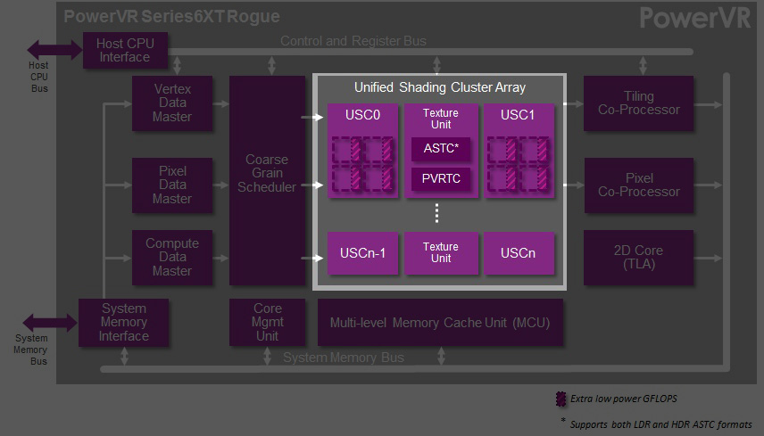
A close analysis of the die shot makes it clear that there are only 4 GPU cores available and not 6, which immediately rules out the 6 core GX6650 we were previously expecting. Instead with 4 cores present this is conclusive proof that Apple is using the smaller 4 core GX6450 on A8, the direct successor to the G6430 used on the A7. GX6450 induces some performance optimizations along with some feature updates – including ASTC support, which Apple’s documentation has already confirmed is present – so its inclusion here is a natural progression for Apple.
On A8 and its 20nm process this measures at 19.1mm2, versus A7’s 22.1mm2 G6430. As a result Apple is saving some die space compared to A7, but this is being partially offset by the greater complexity of GX6450 and possibly additional SRAM for larger caches on the GPU. Meanwhile looking at the symmetry of the block, it’s interesting that the blocks of texturing resources that every pair of GPU cores share is so visible and so large. With these resources being so big relative to the GPU cores themselves, you can see why Imagination would want to share them as opposed to building them 1:1 with the GPU cores.
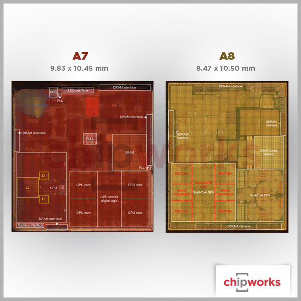
Meanwhile opposite the GPU we have the CPU block. Unlike the GPU the CPU block has seen some significant shrinking, which Chipworks estimates is down from 17.1mm2 in A7 to 12.2mm2 in A8. In A7 Cyclone did not lend itself to easily picking apart the individual CPU cores, and neither does the CPU here in A8. We’ll be looking at the new CPU’s architecture in-depth in our iPhone 6 review, but for now it’s safe to say that while this is definitely derived from Cyclone, Apple has added a few tweaks over the last year that make it an even more potent CPU than the first Cyclone. Meanwhile based on this die shot Chipworks believes that the L2 cache has been reorganized to a per-core design, as there is no obvious single block of L2 on A8 like there was A7.

A8 With PoP DRAM Removed
The final major identifiable block on A8 is once again the SRAM cache memory. On A7 we discovered that this block was 4MB and was responsible for servicing the GPU and CPU. On A8 this block is similarly present and serving the same role. This 4MB of SRAM ends up being quite big despite the shrink from 28nm to 20nm, and while at first glance it seems like it should be larger than 4MB given the relative size, in practice what has happened is that the individual SRAM cells have not shrunk by a full 50%. Chipworks estimates the cell size to now be about 0.08µm2, versus 0.12µm2 on A7, which is closer to a 33% shrink that a 50% shrink. As a result the SRAM cache still takes up a fair bit of space, but the value of being able to serve larger memory requests without having to go off-die continues to be immense.
Apple A8 vs A7 SoCs
 Apple A8 (2014)Apple A7 (2013)
Manufacturing ProcessTSMC 20nm HKMGSamsung 28nm HKMG
Die Size89mm2104mm2
Transistor Count~2B"Over 1B"
CPU2 x Apple Enhanced Cyclone ARMv8 64-bit cores2 x Apple Cyclone ARMv8 64-bit cores
GPUIMG PowerVR GX6450IMG PowerVR G6430
Overall, Chipworks’ analysis points to A8 being fabbed on TSMC’s 20nm process. This makes A8 among the first SoCs to receive the 20nm treatment. Thanks to this smaller node Apple has been able to build in additional features to the SoC while simultaneously shaving off around 15% of their die size. Chipworks estimates the final die size of A8 to stand at 89mm2, versus the 104mm2 for the Samsung 28nm based A7. Chipworks notes that if this were a straight shrink that one would expect the A8 to be closer to 50% the size of A7 (though not all logic can shrink quite that well), which indicates that Apple has spent quite a bit of die size on improving performance through more complex CPU and GPU architectures and miscellaneous feature additions.
Wrapping things up, we’ll be back later this month with our review of the iPhone 6 family and our full analysis of the A8 SoC. So until then stay tuned.

Tuesday, April 15, 2014

Galaxy S5 BOM $256, iPhone $191, $173

IHS released a teardown of Samsung’s Galaxy S5, the estimated bill of materials of $256 BOM keeps going up from previous cell phone generations. See more in the article below;

"IHS found that the Galaxy S3 had a BOM of $205, while the S4 ended up at $233 (LTE version with Qualcomm 600 SoC). On top of that, a Galaxy S series phone costs upwards of $8 to assemble."

While "the iPhone 5S had a BOM of $191 when it launched last September, while the iPhone 5C had $173 worth of components inside its unapologetically plastic body."

Like in Apple's phone DRAM and NAND are a high cost items and as semiconductor manufacturing advance along its learning curve it will increase Samsung margin.
  1. 1080p display is the most expensive component, costing about $65
  2. DRAM and NAND memory is around $33
  3. Unclear how much the Snapdragon 801 SoC costs, should be about $30


See more at iPhone Teardown Updated,  iPhone 5s Teardown, and some more about the processor iPhone A6 Teardown Update


Ron

Insightful, timely, and accurate semiconductor consulting.
Semiconductor information and news at - http://www.maltiel-consulting.com/
Research firm IHS got hold of Samsung’s new flagship smartphone and took it apart to the last bolt to figure out how much it actually costs to build. According to the teardown, the Galaxy S5 has a bill of material (BOM) of $256. 
Of course, this is not the full cost of the device, as it does not cover logistics, R&D, marketing and a range of other expenses that Samsung has to cover before the device makes it to retail.

Galaxy S5 BOM higher than usual


The $256 figure sounds a tad too high. Most flagship phones tend to have a BOM of about $200 or less. Most iPhones usually end up south of $200. For example, the iPhone 5S had a BOM of $191 when it launched last September, while the iPhone 5C had $173 worth of components inside its unapologetically plastic body. 
The Galaxy S5 retails for $699. Samsung does not have as much room to jack up margins as Apple does on the iPhone 5S, but it still has quite a bit more than many manufacturers. What’s more, Samsung’s BOM keeps going up. IHS found that the Galaxy S3 had a BOM of $205, while the S4 ended up at $233 (LTE version with Qualcomm 600 SoC). On top of that, a Galaxy S series phone costs upwards of $8 to assemble.
High-end smartphones are pricey, but at least it’s nice to see that Samsung’s consumers get a bit more value for money with each new generation.

Display remains the priciest component


Unsurprisingly Samsung’s 5-inch 1080p display is the most expensive component in the Galaxy S5. IHS puts its cost at $65. The cost of DRAM and NAND memory is around $33, but it’s unclear how much the Snapdragon 801 SoC costs. IHS puts the price of the Snapdragon 600 used in the S4 at $20, while the big Exynos 5 was estimated to cost $30. The Snapdragon 801 is probably closer to the Exynos in terms of overall cost.
“Inside we see mostly a lot of recycled components that we’ve seen before. There’s really nothing special inside where Samsung is pushing the envelope,” IHS analyst Andrew Rassweiler toldRe/code. “There’s no breakthroughs, there’s nothing earth-shattering. It’s really just a continuation of what has come before.”
However, although there are no breakthroughs, the Galaxy S5 features a few new sensors, including a $4 fingerprint sensor and a biosensor from Maxium, with an estimated cost of $1.45. In addition to the new components which were not used in previous Galaxy S phones, the S5 also features a somewhat sturdier body, which also happens to be waterproof. This probably added a few more bucks to the BOM.