Showing posts with label scaling. Show all posts

Friday, January 23, 2015

Apple Watch battery life, A5-caliber CPU inside

Apple watch battery life is a key factor in how useful this new computer interface will be in our lives. Some information is discussed in the article below. 
"Apple opted to use a relatively powerful processor and high-quality screen for the Apple Watch, both of which contribute to significant power drain. Running a stripped-down version of iOS codenamed SkiHill, the Apple S1 chip inside the Apple Watch is surprisingly close in performance to the version of Apple's A5 processor found inside the current-generation iPod touch,"

More about A5 power consumption is in May 2012 article Apple's A5 Die Shrink, Improve Battery Life, Cut Cost .


 Ron
Insightful, timely, and accurate semiconductor consulting.
Semiconductor information and news at - 
http://www.maltiel-consulting.com/


Apple targets for Apple Watch battery life revealed, A5-caliber CPU inside


Although Apple has said that the Apple Watch will need to be charged nightly, the company has not disclosed any details on how long the wearable's battery will last. For the first time, people with knowledge of the Apple Watch's development have provided us with the specific performance targets Apple wants to achieve for the Apple Watch battery, but the actual numbers may fall short of those targets.

According to our sources, Apple opted to use a relatively powerful processor and high-quality screen for the Apple Watch, both of which contribute to significant power drain. Running a stripped-down version of iOS codenamed SkiHill, the Apple S1 chip inside the Apple Watch is surprisingly close in performance to the version of Apple's A5 processor found inside the current-generation iPod touch, while the Retina-class color display is capable of updating at a fluid 60 frames per second.
Apple initially wanted the Apple Watch battery to provide roughly one full day of usage, mixing a comparatively small amount of active use with a larger amount of passive use. As of 2014, Apple wanted the Watch to provide roughly 2.5 to 4 hours of active application use versus 19 hours of combined active/passive use, 3 days of pure standby time, or 4 days if left in a sleeping mode. Sources, however, say that Apple will only likely achieve approximately 2-3 days in either the standby or low-power modes…

Apple has also been stress-testing the Apple Watch's battery life with pre-bundled and third-party applications. Our sources say that Apple is targeting 2.5 hours of "heavy" application use, such as processor-intensive gameplay, or 3.5 hours of standard app use. Interestingly, Apple expects to see better battery life when using the Watch's fitness tracking software, which is targeted for nearly 4 hours of straight exercise tracking on a single charge.

As Apple is positioning the Apple Watch as a timepiece, the company has conducted numerous tests to determine how long it can run purely in time-keeping modes. We're told that the Watch should be able to display its clock face for approximately three hours, including watch ticking animations, if nothing else is done with the device. However, it's unlikely that most people would actually keep the Apple Watch clock face turned on for even three hours straight in a single day. When the Watch screen is not in use, the display is powered off, and the clock demands much less energy.

Considered separately, the active use app, clock, and fitness numbers sound very low, but the reality is that people will passively wear the Apple Watch for most of the day, actively interacting with it only for short periods of time. That's why the Watch will be able to last the average user roughly a day on a single charge. We're told that Apple has been shooting for roughly 19 hours of mixed usage each day, but that the company may not hit that number in the first generation version.

Sources tell us that battery life has remained a source of concern for Apple over the past year, and was a contributing factor for Apple pushing back the retail launch from an originally planned late 2014 to early 2015. To test real-world performance in a variety of conditions, the company has circulated a surprisingly large number of test units of the Watch: nearly 3,000 are said to be currently roaming around, mostly the stainless steel variant.
Apple has also been working to perfect the MagSafe-based inductive charging mechanism for the Watch, which sources indicate was responsible for slower-than-expected recharging times that hopefully will be fixed in time for the product's release. The company has developed both plastic and stainless steel versions of the circular charger, potentially one for the $349 aluminum and plastic Apple Watch Sport, and the other for the higher-end models. It's unclear at this point whether the company will sell multiple versions of the charger, as Apple has only shown the metal variant, though the Apple Watch Edition is said to ship with a special box and charging dock that may incorporate the stainless steel MagSafe connector.

As of earlier this month, the Apple Watch is on track to ship by the end of March. We previously detailed how the Watch will integrate with the iPhone via an iOS 8.2-based Companion application.

Thursday, December 4, 2014

3D Flash Race:Intel vs Samsung

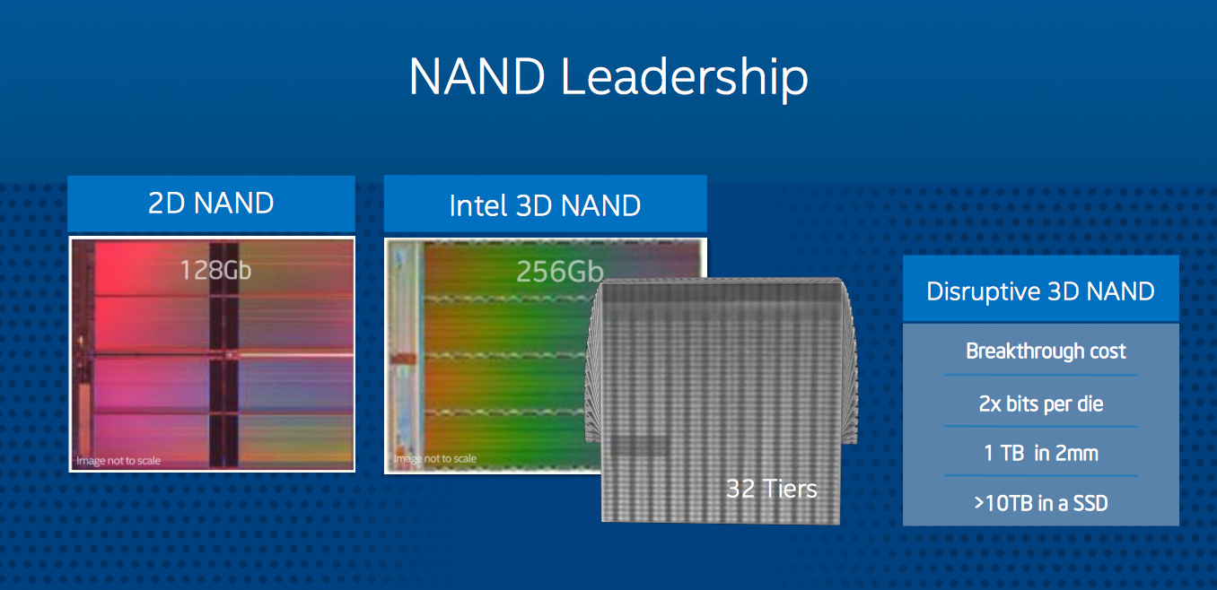
Following Samsung development of V- NAND Intel introduce their version of 3D NAND (see below). One of the benefits of 3D flash memories is the capability of using larger design rules such as 30-40 nm instead of scaling the design rules to smaller than 20nm.

One of the key problem of shrinking to smaller design rules than 20nm is the cost and complexity of multi-patterning photolithography and EUV lithography difficulties (ASML: Next-gen chipmaking tool ready forproduction in 2016 ). In addition, the reliability of the flash memory degrades when the memory cells become too close to each other.

"Samsung consciously went from a 24-layer 128Gbit MLC die to a 32-layer 86Gbit MLC die. In other words, Samsung could have upped the die capacity to ~170Gbit by just adding the extra layers, but the company chose to go with a smaller die instead. Smaller capacity dies have advantages in performance (higher parallelism) and applicability because eMMC/microSD devices have very strict die size constraints, "

Samsung only use 24 layers in fabricating the chips in order to increase the yield, which reduces the cost of working dies on each wafer. Adding layers that has to be manufactured with precise alignment and low defect density lengthen the learning curve of fabricating working dies. Intel is trying to catch up with Samsung which is already making the second generation of 3D NAND (Samsung 3D Process Pioneers Next Gen Semiconductor Devices ).


Ron
Insightful, timely, and accurate semiconductor consulting.
Semiconductor information and news at - http://www.maltiel-consulting.com/


Intel's 3D NAND to Ship in H2'15: 256Gbit Die

 & 32 Layers

by Kristian Vättö on November 25, 2014 5:20 AM EST
Last Thursday in its annual Investor Meeting Intel revealed the first details of its 3D NAND technology and announced that it will begin the shipments of 3D NAND in the second half of 2015. While Intel's investment in 3D NAND hasn't been a secret, the company has been relatively quiet about any specifics and the vital specs such as the number of layers and die capacity have remained unknown. In Thursday's webcast, Rob Crooke, Senior VP and General Manager of Intel's non-volatile memory group, disclosed that Intel's first generation 3D MLC NAND die will be 256Gbit (32GB) in capacity and will consist of 32 layers. The technology also enables a 384Gbit (48GB) TLC (3-bit-per-cell) die as we have learned over the years.
Intel claims that its 3D NAND is the most cost effective on the market and bases this on the fact that its die is 256Gbit whereas Samsung's is only up to 128Gbit at the moment. I'm not sure if I buy Intel's claim because while it's true that a higher capacity die results in higher array efficiency (i.e. peripheral circuitry takes less area), Samsung consciously went from a 24-layer 128Gbit MLC die to a 32-layer 86Gbit MLC die. In other words, Samsung could have upped the die capacity to ~170Gbit by just adding the extra layers, but the company chose to go with a smaller die instead. Smaller capacity dies have advantages in performance (higher parallelism) and applicability because eMMC/microSD devices have very strict die size constraints, so that might be a part of the reason why Samsung's strategy is so different from Intel's and Micron's. 
NAND Die Size
As the graph above shows, Intel's/Micron's NAND dies have historically been larger than the competitors', so the die capacity alone isn't enough to dictate whether Intel's 3D NAND is more cost efficient than Samsung, especially because both have 32 layers. Unlike Samsung, Intel didn't reveal the lithography that is used to manufacture the 3D NAND, but I would say it's safe to assume that the lithography is in the order of 30nm or 40nm because the whole idea of 3D NAND is to move away from multi-patterning to cut costs and with today's technology the smallest pitch of single-patterning is somewhere between 30nm and 40nm. Either way, it will be very interesting to see how Intel's 3D NAND stacks up against Samsung's because there are also some structural differences that affect the production cost as well as performance and endurance, but I'll save the structural analysis for a future article.
Intel said that 3D NAND technology will enable +10TB SSDs in the 'next couple of years', but it wasn't clear whether that is with first generation 3D NAND or some later generation with more layers and higher die capacity. Currently Intel's lineup tops out at 2TB (P3700 & P3600) with a 128Gbit die, so the 256Gbit die alone isn't enough to bring the capacities above 10TB. With effective controller development it should certainly be possible to build a 10TB SSD with a 256Gbit die, although I'm still inclined to believe that Mr. Crooke was referring to second or third generation 3D NAND with his statement. 
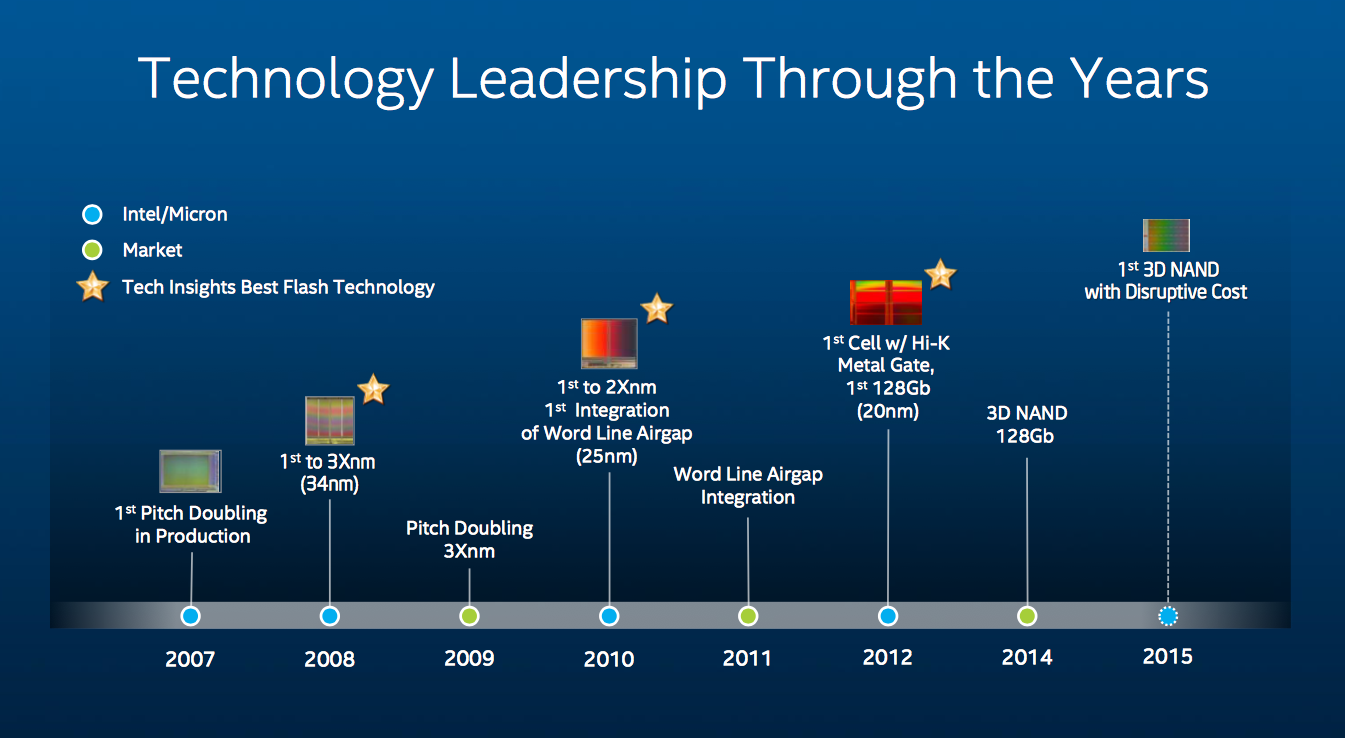
Similar to Intel's previous NAND efforts, 3D NAND has been jointly developed with Micron and will most likely be manufactured in the co-owned Utah plant as Intel sold its share in other fabs a couple of years ago. Interestingly enough, Mr. Crooke said that they also have the ability to bring 3D NAND production to an Intel fab, although to me that sounded more like a statement of technological possibility rather than a hint of future strategy. I wouldn't rule it out, though, but like Mr. Crooke said in the Q&A, Intel needs to have significant competitive advantage for it to make sense. In the past Intel's NAND technologies have generally been slightly ahead of the rest of the industry, but at least as of now Intel doesn't seem to have any substantial advantage in 3D NAND technology as Samsung is already shipping a 32-layer die and will likely ship a 48-layer die before Intel ships its 32-layer product.
All in all, we'll likely get more crumbs of information as the second half of 2015 gets closer. Given Intel's recent SSD strategy, I expect 3D NAND to first find its way to enterprise-class SSDs, but we'll see soon enough.

Thursday, September 5, 2013

Hynix Fab Fire Manufacturing Implications

Yesterday Hynix had a fire at their  at its Wuxi,China, plant

It looks that the fire would have only short term impact on NAND production since it "mainly in the air purification facilities on the rooftop of the fab and created a disproportionate amount of smoke".

If its true that it only impacted the air filtration system, production is dependent on how quickly Hynix can fix/ replace the air purification components, and the magnitude of the damage to the air filtration inside the fab.

"TrendForce said the fire could impact SK Hynix's production procedures "considerably" in the near future, particularly since the Wuxi plant manufactures almost 50 percent of the company's monthly output of 260,000 wafers and contributes over 10 percent of the world's DRAM wafer production. It added that the facility is responsible for producing 100,000 of its PC DRAM and 30,000 mobile DRAM. 
"The potential damages imparted on the supply end should not be underestimated," the research firm said. Should SK Hynix's main production line be stalled, the shipment of almost 11 million laptops and 10 million smartphone units will be affected within the span of a month, Trendforce said. "....
http://www.zdnet.com/sk-hynix-china-plant-fire-wont-affect-chip-production-7000020281/

Short term, Hynix production will depend on how quickly Hynix can get a new system installed and running.

Longer term impact depends on;

1. Market demand for year end for consumer NAND, SSD (tablet /iPad growth vs . PC stagnation, and mobile phones)

2. The real short term pace of demand for server farms, cloud SSD products.

Ron


 Insightful, timely, and accurate semiconductor consulting.
Semiconductor information and news at -
http://www.maltiel-consulting.com/

Monday, July 15, 2013

Update: Samsung Fab. Apple A9 Processor?

It make sense for Apple to hedge it bets and use both TSMC and Samsung (see article below). It doesn't hurt that Samsung already spends 7 Billion dollars on next generation fab.

Update: GlobalFoundries Should Appeal to Apple. Not likely that Apple will get into chip making business. However all these rumors help apple negotiate with various potential partners.

Ron
Insightful, timely, and accurate semiconductor consulting.
Semiconductor information and news at - http://www.maltiel-consulting.com/


Apple Reportedly Signs Deal with Samsung for 14-nm A9 Chips Starting in 2015


The Korea Economic Daily reports that Apple and Samsung today officially signed an agreement that will see the two companies working together on future A-series chips for Apple's iOS devices, with the deal specifically covering A9 chips based on a 14-nanometer process node starting in 2015. The claim comes just weeks after Taiwan Semiconductor Manufacturing (TSMC) confirmed a deal with Apple to begin producing A-series chips in 2014.
Samsung Electronics had supplied the AP [application processor] to Apple since 2007 but lost the contract to supply 20 nano AP A8 chips to Apple to Taiwan's TSMC last year when it was engaged in patent disputes with Apple. Samsung Electronics developed state-of-the-art 14 nano models ahead of its rival TSMC, regaining the order from Apple.
A previous report about Apple's agreement with TSMC had indicated that it was a three-year deal covering not only Apple's future A8 chip but also A9/A9X chips. The Wall Street Journal's report had indicated that Samsung would remain Apple's primary supplier through next year as TSMC began ramping up its production. 

As a result, it is unclear whether today's deal will see both TSMC and Samsung producing A9 chips for Apple or if Apple has already shifted gears to return to Samsung as its primary supplier as part of its long-term roadmap. 

Apple has reportedly been seeking to reduce its reliance on Samsung as a component supplier as the two companies have become fierce rivals in both the mobile marketplace and in the courtroom. The two companies have, however, continued working together in several areas, particularly where Samsung's competitors in the component market are unable to match its technology, production capacity, or pricing. 

The shift to TSMC for production of the high-profile main chips for Apple's iOS devices had been viewed as breaking one of the most significant remaining ties between Apple and Samsung, but it appears that Samsung has been able to bring Apple back into the fold by leading the charge to 14-nm chips. With partnerships with both Samsung and TSMC, it appears that Apple should be well-positioned to take advantage of whichever company takes the lead in developing the latest technologies. 

Late last week, it was reported that Apple had bought into a fab, perhaps with an eventual goal of producing its own chips for its mobile devices, although any such move is almost certainly years away given the need to ramp up expertise and facilities for such production.

Thursday, December 13, 2012

Apple iPad 4 – A6X Tear-down

Chipwork's teardown of the new Apple iPad 4 reveals a major redesign of the graphic processor (GPU). The much larger area dedicated to the GPU and wider interface of the DRAM improves the display and touch screen performance of the iPad 4. It probably also helps prolong battery life.


" The A6 is 94mm2 while the A6X is 123mm2 – a full 30% larger.So where did that extra area go? Well, firstly, it did not go to the CPU core. The A6X uses the identical CPU to the A6. Same size, same layout. This is not surprising given that the prior CPU used custom layout techniques, and therefore it would be a huge amount of work to redesign so soon. Much of the extra area has gone to the GPU cores which are up from 3 to 4. More notable is that each of these GPU cores is much larger.On the A6X each GPU core is 8.7mm2 while the A6 GPU cores are only 5.4mm2. The overall area occupied by the A6X GPU cores is more than double that of the A6!

So we see that of the 29 mm2 of new area on the A6X, a full 18.6 mm2 is the result of the increased quantity of graphics processing. Impressive!

Additionally, if you look closely at the GPU cores (which our high magnification scopes allow us to do), we can see they are actually split into sub-cores themselves. Each GPU core is sub-divided into 9 sub-cores (2 sets of 4 identical sub-cores plus a central core). This could be done to allow for more efficient parallel processing, or to allow for a higher maximum clock rate. In either case, these GPUs should result in some blazing graphics on your iPad.

Other items of note:

It looks like the A6X has double the SDRAM interface width of the A6 (again likely to allow for greater graphics processing power).

Other than the CPU, it appears all the other digital cores have new layouts. This chip is not just a minor tweak from the A6, a lot of work has gone into this.

Apple has reduced the number of core PLLs needed from 9 on the A6 to 8 on the A6X. However they have moved them close to the middle of the chip which may allow for better control over clock skew across the chip.

Many of the analog and interface cores have been reused from the A6, however there are also some new interface blocks."

Additional information

Ron Maltiel   www.maltiel-consulting.com

Tuesday, November 13, 2012

FinFET Layout Design Rules and Variability


It is not simple to design circuits with FinFET transistors. Layout, 3D dimensions, and shape considerations are described in the article below. Some additional information about Intel's 22nm 3D Tri-Gate FinFETs Transistors.


Ron
http://www.maltiel-consulting.com/


FinFET structure design and variability analysis enabled by TCAD

Victor Moroz, Synopsys Inc.

10/8/2012 10:14 AM EDT

The introduction by Intel of FinFET transistors at the 22nm mode culminates many years of research and development of a replacement transistor to the immensely successful planar MOSFET whose progressive miniaturization is largely responsible for the electronics revolution. The need for a successor to the planar MOSFET had long ago been identified. Starting with the 90nm process node, improved transistor performance was achieved with the introduction of stress into the transistor channel in a way that boosts the speed of the electrons and holes traveling within it. However, controlling the transistor leakage in the off-state became progressively more difficult. Keeping the electrons and holes under the electrostatic control of the gate electrode is key to controlling leakage current, but a number of so-called short channel effects undermine the gate control. The introduction of high-k dielectrics as the gate insulator at the 45nm process node effectively extended the life of the planar MOSFET for another two process nodes, but by the 22nm process node the planar MOSFET could hardly offer an attractive balance of performance and leakage.


Intel’s FinFETs thus mark the first fundamental change in transistor architecture since the time when the MOSFET replaced the bipolar transistor as the transistor of choice for logic applications. Its performance improvements over the preceding process node (see table) are a clear indication of the promise this technology holds. Although the manufacturing of FinFETs is more complex than manufacturing of its planar predecessor, Intel’s introduction is a testament to the inevitability of these devices....   More at FinFET Layout Design and Variability

Thursday, November 1, 2012

Intel's 14nm Process and Manufacturing Roadmap


With foundaries venturing into the FinFET devices it is interesting to see Intel's direction.


The article below with Mark Bohr, senior fellow at Intel, review the road map pertaining to a wide range of manufacturing and design issues. Some of the key points in the article are:

* Intel is sticking with bulk CMOS instead of SOI.

* FinFET transitors are scalable to 14nm process.

* "3D stacked die have advantages, but only for certain market segments. You have to be very clear about what problem and what market segment you’re trying to serve. For a small handheld application where a small footprint and form factor are key and power levels are low, it probably makes good sense to use 3D stacking. For desktop, laptop and server applications where form factor isn’t as valuable and power levels are higher, 3D stacking has some problems that make it not an ideal solution"

Additional information about Intel's 22nm at Tutorial: Intel 22nm 3D Tri-Gate FinFETs Transistors and at Intel’s 22-nm Tri-gate Transistors Exposed


Ron
http://www.maltiel-consulting.com/


Deep Inside Intel
By Ed Sperling

Semiconductor Manufacturing & Design sat down with Mark Bohr, senior fellow at Intel, to talk about a wide range of manufacturing and design issues Intel is wrestling with at advanced nodes—and just how far the road map now extends.


SMD: Will EUV make 10nm? And if it doesn’t, what effect will that have on Intel?

Bohr: For a process module as critical as lithography, Intel always has more than one option we pursue. In this era, the options are either EUV or 193nm immersion with multi-patterning.


SMD: How about directed self-assembly?

Bohr: That’s not a universally usable approach. You still need to define some layers with direct patterning, not a self-assembly technique. That’s a niche direction that will not replace these mainstream lithography techniques, but there may be some layers where it can complement the normal patterning techniques.


SMD: What’s your opinion about the future of the foundry business?

Bohr: The traditional foundry model is running into problems. In order to survive, the foundries will have to become more like an integrated device manufacturer. Even some of the chief spokespeople for the foundries have said something similar. The foundry model worked well when traditional scaling was being followed and everybody knew where we were headed. In this era, where you continually have to invent new materials and new structures, it’s a lot tougher being a separate foundry and maskless design house. Being an IDM, we have design and process development under one roof. That’s really a significant advantage.


SMD: Can even Intel afford to be an independent IDM? The cost of building state-of-the-art fabs at future nodes is astronomical.

Bohr: Yes. We have the volume and the products that can fill multiple fabs.


SMD: But you’ve also opened up your fabs to at least a couple customers. Are you planning on extending that? ,

Bohr: Our motivation is that we know we have great process technology, and partnering with other strategic companies can be a win-win situation. We can sell our technology and make more money off what we’ve developed, and they can have some very compelling products. It’s not Intel’s goal to be a general-purpose foundry, but we will be partnering where it makes strategic sense.


SMD: Is Intel sticking to bulk CMOS or will move to new materials such as fully depleted SOI?

Bohr: We see more advantages in bulk than SOI. I won’t say SOI won’t be in the future. There may be some device structure that is better done in SOI than bulk. But I don’t see than happening right now. When we first announced that we were making TriGate or finFET devices at 22nm, we said we’re making these devices on SOI, as well. But we think there are cost advantages to doing TriGate on bulk rather than SOI. That’s our plan for the foreseeable future.


SMD: What comes after the current finFET?

Bohr: The finFET is scalable to 14nm.


SMD: But if you’re at 22nm, 14nm isn’t very far away, so you’ve got to be working on the next step.

Bohr: For Intel, you’re right. For other companies, it’s many years away. For 10nm, which is where I’m spending most of my time these days, I know we have a solution. I can’t elaborate at this point.


SMD: At 10nm aren’t you running into quantum effects?

Bohr: Everything gets different and tougher, but the problems are solvable—at least at that generation.


SMD: How far ahead can you see?

Bohr: I know we can get to 10nm. Beyond that, our research group is working on solutions for 7nm and 5nm. I have confidence we’ll have solutions for those. But by the time we’re down to 5nm we’ll be looking at non-familiar devices and device structures. That’s what we’ll have to do to get down to that level.


SMD: Where do stacked die fit into your roadmap?

Bohr: 3D stacked die have advantages, but only for certain market segments. You have to be very clear about what problem and what market segment you’re trying to serve. For a small handheld application where a small footprint and form factor are key and power levels are low, it probably makes good sense to use 3D stacking. For desktop, laptop and server applications where form factor isn’t as valuable and power levels are higher, 3D stacking has some problems that make it not an ideal solution.


SMD: Along those lines, does Intel see the smart phone and small mobile device market as a key direction?

Bohr: Intel is very serious about getting into the smart phone and tablet markets. We are a very different company from what we were five or six years ago. We are developing process technologies, but also products, that span a much wider range of performance and power than anywhere in our history. We’re not just after the high-performance desktop. We’re developing products that support 100-watt server chips down to sub-1 watt smart phone chips.


SMD: There are a number of interesting techniques Intel is working with, such as near-threshold computing. How will power management start changing inside these chips?

Bohr: When you’re talking about developing a smart phone chip that is ultra low power that also provides improved performance features that the market expects, you have to pull every trick out of the bag. You need great transistor technology, great package technology, great CPU architectures, the ability to turn off parts of the chip when you don’t need them so you’re saving power, the software links with the chip design so the software knows when to throttle power down. You need transistors, CPU architecture and software to be effective in that space.


SMD: How many cores will be required in the future?

Bohr: It depends on the market. In the server market, the more cores you can pack on the better. But in desktops, laptops and smart phones, there’s probably a limit to how many cores are practical. It’s not one. It’s probably several.


SMD: But less than eight?

Bohr: Yes, probably less than eight. But when you talk about the number of cores and computing engines, it depends on whether you’re dealing with traditional computing tasks where four cores are better than two cores. If you’re talking about execution engines in a graphics processor, clearly you want more cores.


SMD: What does this do for Intel’s platform strategy, particularly as you go after many markets with very specific needs?

Bohr: Even for Intel there are probably an optimal number of chip designs. It’s not like in the past where we tried to make one size fit all or have one chip serve multiple markets. But on the other hand, trying to design and manufacture dozens of very different designs in a generation is also impractical. There’s an optimal number of designs, although I don’t know what that number is, that can best meet the market requirements. You want to make as few iterations between the different designs as you can or re-use the cores or some of the circuit blocks between the different chips so you’re not completely redesigning it.


SMD: Are there other materials being considered for transistors?

Bohr: Our research group has been publishing papers about using 3-5 materials http://en.wikipedia.org/wiki/List_of_semiconductor_materials for the channels. You deposit indium phosphide or gallium arsenide layer on top of silicon to make a transistor on the surface. It’s still a silicon wafer, but you’re looking at depositing more exotic materials. That’s new and different and it may happen, but it’s not yet fully resolved how good that approach may be.


SMD: Has the priority for what you’re designing into a chip changed? Is it still all about performance, or has power overtaken that?

Bohr: Ten or 15 years ago, performance was the main goal in developing a new process technology. That really has gone away as the No. 1 priority. We still strive to provide a performance boost with each new technology, but there’s much more emphasis on improving power or efficiency on each new generation. We do that by reducing active power for the work a chip does. That’s a much more important goal for us today. Part of the reason is that the market has shifted from desktop applications to more mobile products. The first transition was from desktops to laptops. Now the move is to put things into smart phones. Today’s consumer wants computing power he can hold in his hand in the form factor of a smart phone and a tiny battery. He wants the performance he had on his laptop only three or four years ago. That’s what we shoot for.


SMD: That shifts the biggest challenge to the architecture, right?

Bohr: Yes. Whether it’s low-power, low-leakage transistors or a more efficient core architecture—or linking that with more efficient software.


SMD: What becomes the next big bottleneck?

Bohr: We have lots of challenges. Lithography is the key challenge in making transistors smaller. Whether EUV will happen on time or we have to extend immersion using multiple patterning. But when you make transistors smaller they don’t become less leaky. In fact, the opposite is true. You have to continually invent new structures and materials to allow feature-size scaling, which is critical for active power reduction and for cost.


SMD: But wires don’t scale well. How do you deal with that?

Bohr: RC delay gets worse as you scale, compared with transistors, which tend to get faster as you scale down. The industry has had 20-plus years of struggling with that problem. One way we’ve addressed that is that we’re no longer striving for very high operating frequency, especially in the phone market where 2 or 2.5GHz would probably be sufficient. That’s one advantage. The other advantage is that the average size of the chips is smaller in these laptop and cell phone applications so you don’t have interconnects traveling a long distance across a large chip. Instead, it’s a more compact chip so the signals don’t have to go as far. But even with those chips, we still have a challenge of performance from the interconnect. We have to be clever about what pitches we choose. Some of the lower layers are dense pitch, where density is important. Some of the upper layers are coarser pitch, where performance is important. We’re also continuing to drive down interconnect capacitance by employing lower-k dielectrics.


SMD: Is the interconnect becoming more problematic?

Bohr: If you talk to a designer 10 years ago you would have heard the same thing. Maybe now they’re saying, ‘This time we’re really serious.’


SMD: How about new interconnect technology?

Bohr: It’s hard to replace copper and low-k other than by making lower k. But at least in the low-power cell phone market, stacking chips does help to minimize some of the interconnect issues, particularly between the logic and the memory chips.


SMD: You’re referring to through-silicon vias?

Bohr: Yes.


SMD: So if Intel is planning to get into that market, the company is experimenting with that technology right now?

Bohr: Yes, and we’ve been public about exploring TSV and 3D technology for a couple years. Although there are some challenging technology aspects, the real issue is cost. Doing TSVs and stacking chips—especially these custom Wide I/O chips—is expensive. So this might be a better engineering solution in terms of density, performance and power, but will the market bear the added cost? Not all markets will bear the higher cost.

Tuesday, October 30, 2012

Apple's A6X Processor 32nm Process Advantages

Apple's latest iPad 4 processor comes with its latest processor: an A6X, which Apple says delivers twice the CPU and graphics performance as the A5X. See below some details about Apple's A6X processor.

"Apple moved from a 45nm process to a more power-efficient 32nm process. Instead of keeping performance the same and decreasing the iPad's thickness and weight, Apple instead chose to double its performance without sacrificing all-day battery life."

More about Apple's optimizing process and design at iPhone A6 Teardown Update

Ron
http://www.maltiel-consulting.com/


Deducing details about Apple's A6X processor


Apple promises double the CPU and graphics performance over the A5X, but how?

by Chris Foresman - Oct 23 2012, 3:25pm PDT


As usual, Apple didn't share many specifics about its new A6 "Extreme" (A6X) processor, which powers the fourth-generation iPad. However, by looking at Apple's claims that it's "twice as fast" as the A5X-powered third-gen iPad, it may be possible to deduce what's inside.

According to Apple, the A6X processor "delivers up to twice the CPU and graphics performance of the A5X chip." In other words, the dual-core CPU can process data twice as fast as the dual-core 1GHz, Cortex A9-based A5X. It can also churn through OpenGL triangles and textures at twice the rate of the PowerVR SGX543MP4 in the A5X. So how did Apple do that?

Looking at CPU power for the moment, we already know that Apple designed a custom ARM-based core for the A6. Running at 1.2GHz in the iPhone 5, two A6 cores run twice as fast as two 800MHz A5 cores in an iPhone 4S.

However, the A5X in the third-gen iPad was clocked at 1GHz. That means Apple is clocking the A6X higher yet. Given that architectural improvements account for some of the speed increase, Apple only had to clock the iPhone 5 at 150 percent to achieve double the compute performance of the iPhone 4S. With this in mind, we believe Apple is clocking the A6X's CPU cores at 1.5GHz.

Examining the GPU is slightly different. Apple already jammed four SGX543 GPU cores into the A5X in order to achieve performance parity with the two SGX543 GPU cores in the A5 chip that powers the iPad 2. The extra GPUs were needed just to keep up with the 2048×1532 pixel Retina display, so these did not offer any graphics performance improvement. However, Apple says that the A6X pumps pixels twice as fast.

Apple could be using a newer-generation PowerVR core, but that appears to be very unlikely. Only one announced processor is known to use a PowerVR Series6 design, and it won't even begin sampling until 2013. Given that Apple just released the A6 a month ago, we're confident Apple is still using the same SGX543 core.

Here's what we know about the PowerVR SGX543 core's performance: it scales almost linearly with the number of cores and clock speed. So to double the performance, Apple would either have to double the number of cores to eight or double the clock speed of each of the four cores. Apple says that the A6X has "quad-core graphics"—the same as the A5X—so Apple clearly boosted the clock speed. Since the GPUs in the A5X were clocked at 250MHz, we believe that Apple has clocked the SGX543 cores at 500MHz.

Given the significant boosts in clock frequency—150 percent for the CPU cores, and 200 percent for the GPU cores—you may be wondering how Apple can still promise a 10-hour battery life. After all, the iPad still has the exact same 42.5Whr battery, but the processor is twice as powerful. The power savings come from the same place as we saw in the iPhone—Apple moved from a 45nm process to a more power-efficient 32nm process. Instead of keeping performance the same and decreasing the iPad's thickness and weight, Apple instead chose to double its performance without sacrificing all-day battery life.

Of course, we won't know how accurate our educated guesses are until one of the new iPads can be thoroughly benched, and the A6X's architecture is analyzed by the likes of Chipworks. However, we feel confident suggesting Apple has mated two A6 ARM cores running at 1.5GHz with four PowerVR SGX543 cores running at 500MHz. Given the performance results we saw with the iPhone 5, we expect the updated iPad will remain at the top of the tablet performance heap for some time.

Saturday, October 6, 2012

Semiconductor Foundries:Strong Q2, but Slowdown..

The article below discusses foundries' strong Q2  results, while predicting a slower Q3.

"Pure-play foundry semiconductor manufacturers enjoyed a robust second quarter thanks to enthusiastic consumer purchasing of wireless products like mobile handsets and tablets, but the industry is slowing down in the second half of 2012 as economic tremors roil the supply chain"

However, I wonder about the impact of the slow ramp-up of manufacturing wafers using the 28nm manufacturing process in Q2 and Q3. There is pent up demand for wafers built using the 28nm process which could impact Q4 (see April 2012 comments Qualcomm and Nvidia 28 nm Wafers? Shortage... and March 2012 comments Nvidia: TSMC 20nm Essentially Worthless). The lack of 28nm wafers negatively impacted Qulacomm, Nvidia and other companies.

Another potential upside for the second half of 2012 is the introduction of window 8 and its impact on demand for tablet computers.

Ron
http://www.maltiel-consulting.com/


Semiconductor Foundries Enjoyed Strong Q2, but Slowdown Looms


Global economic uncertainties and a wary buying public will dampen prospects until mid-next year

Len Jelinek October 2, 2012
Pure-play foundry semiconductor manufacturers enjoyed a robust second quarter thanks to enthusiastic consumer purchasing of wireless products like mobile handsets and tablets, but the industry is slowing down in the second half of 2012 as economic tremors roil the supply chain, according to an IHS iSuppli Semiconductor Manufacturing & Supply market tracker report from information and analytics provider IHS.

Revenue for pure-play foundry suppliers—companies whose entire business involves producing semiconductors for other firms—reached $7.8 billion in the second quarter, up 16 percent from $6.7 billion in the first quarter.

The second-quarter expansion will prove to be the strongest this year, as forecasts show a slowdown occurring during the next two quarters. Revenue of $8.3 billion is projected for the third quarter, equivalent to a weaker sequential growth of 8 percent. A seasonal decline of 5 percent in the fourth quarter then will follow, dropping revenue for the period to $7.9 billion.


The strong showing of the second quarter this year is atypical. Even though the third quarter is the largest revenue period for the foundry sector, a new pattern of manufacturing has emerged, with initial product shipments from foundry suppliers for new design wins now moving from the third quarter to the second. This shift is related to end suppliers introducing next-generation wireless products, like cellphones and tablets, earlier in the year in order to capitalize on sales during a longer period—one lasting three quarters, instead of the usual two quarter time frame that traditionally starts at the beginning of the second half.

As a result of the shift, foundry suppliers must start to adjust technology development and factory expansion plans to mirror these changes. Shipments in the third quarter are now also a direct reflection of second-quarter performance.


Impending Q3 concerns on the horizon

The third quarter this year, however, is when manufacturers can begin to anticipate a reduction in orders, IHS iSuppli predicts. While demand for advanced technology will continue to drive overall revenue growth within the industry, the effects of external influences—such as a deteriorating global economy—will start being felt. The financial issues in Europe, for instance, will leave their mark in Asia as well as North America, and shaky consumer confidence throughout the world will result in an uncertain outlook for holiday spending. The end result would be a greater amount of inventory left throughout the industry.

Questions also abound on whether consumers will be willing during the next few months to pay for the latest technology rollouts. Unlike last year when holiday shoppers were enticed to purchase lower-cost electronics resulting from excess inventory, this year will be different, with consumers seeing a complete set of new electronics offerings focused on mobile communications, including next-generation tablets, feature-rich smartphones and Ultrabooks with the soon-to-be-launched Windows 8 operating system.

And while the potential exists for increased sales in the second half, any projected upticks are likely to be insufficient to drive major revenue increases for foundry players. This is because any innovative products introduced at this time will be too late to have any tangible effect on revenue for the remainder of the year.

At the current production pace, foundry manufacturing run rates will be negatively affected through the first quarter next year lasting until the first half of the second quarter, IHS iSuppli believes. The industry will begin to recover after that, with the third quarter next year anticipated to grow by a sequential 10 percent.

Friday, July 6, 2012

Apple's next iPhone: Quad-Core Processor

The article below refer to a rumor that next iPhone would have a Quad core designed by Samsung. It is not very likely that Apple would abandon their in house development for a replacement for the A5 processor . Apple own specialized processor give them an edge with optimized display and battery life. See more in my May blog Apple's A5 Die Shrink, Improve Battery Life, Cut Cost .


Ron


Apple's next iPhone rumored to feature quad-core processor
http://www.appleinsider.com/articles/12/07/05/apples_next_iphone_rumored_to_feature_quad_core_processor.html

Apple's next-generation iPhone will be powered by a quad-core ARM processor based on Samsung's Exynos 4 architecture, according to a new report.

The claim comes from the sometimes-reliable DigiTimes, which cited its usual industry sources from the Far East in a report issued on Thursday. Other details on the rumored processor, including clock speed or graphics processing capabilities, were not presented.

Last year's iPhone 4S features a custom dual-core processor clocked at 800 megahertz, dubbed by Apple the "A5." That chip was first introduced months earlier in the iPad 2, where it ran slightly faster at 1 gigahertz thanks to a larger form factor with a bigger battery.

With the third-generation iPad launched this year, Apple didn't unveil a true next-generation chip, choosing instead to name the processor the "A5X," suggesting an evolutionary upgrade over its predecessor. That CPU is based around Samsung's 45-nanometer low-power architecture, also found in the A5 CPU in the iPhone 4S and iPad 2.

The main change with the A5X was an updated integrated graphics processor. While the CPU remained dual core, the GPU was upgraded to quad core in order to push the 3.1 million pixels found on the tablet's high-resolution Retina display.

If Apple does build a quad-core ARM CPU for its next iPhone, the upgrade could presumably be significant enough to earn the chip the "A6" distinction. DigiTimes said Apple's expected introduction of a quad-core iPhone will help "heat up" competition with other quad-core smartphones.

Samsung, HTC, LG and Meizu all launched quad-core smartphones in the second quarter of 2012, most notably Samsung's Galaxy S III, the latest flagship handset for Google's Android mobile operating system. However, the quad-core Galaxy S III has thus far only been available in international markets, while the 4G LTE-capable model released in the U.S. features a dual-core Snapdragon S4 processor. Next week, Samsung will launch a quad-core LTE Galaxy S III, but only in Korea.

More quad-core smartphones are expected to be introduced in the second half of 2012, thanks to volume production of chips from Qualcomm.

Wednesday, May 9, 2012

Nvidia #1 at TSMC Fab? Nvida has Priority for 28nm capacity

"TSMC has given priority to Nvidia for 28nm capacity, according to industry sources" (see below).

Nvidia has been unsatisfied with TSMC's 28nm process
Photo: Monica Chen, Digitimes file photo


Complaining publicly did not hurt - see March 26, 2012 blog Nvidia: TSMC 20nm Essentially Worthless 


Ron


TSMC gives priority to Nvidia for 28nm capacity

http://www.digitimes.com/news/a20120509PD211.html?mod=2
Monica Chen, Taipei; Joseph Tsai, DIGITIMES [Wednesday 9 May 2012]

Taiwan Semiconductor Manufacturing Company (TSMC) has given priority to Nvidia for 28nm capacity, according to industry sources.
Since Nvidia has been unsatisfied with TSMC's 28nm process, while the company has also not refuted rumors that the company may cooperate with Samsung Electronics or Globalfoundries, TSMC, to sooth Nvidia, has put the GPU maker on its supply priority, allowing Nvidia to be able to release its 28nm GPUs on schedule in May and June.
The same situation has also happened previously with Qualcomm, which had said it would consider outsourcing orders to other wafer foundries, and successfully gained TSMC's promise for supply priority.
With both Qualcomm and Nvidia achieving supply priority from TSMC, players that are also waiting for TSMC's 28nm capacity, are expected to be affected.


Friday, May 4, 2012

Apple's A5 Die Shrink, Improve Battery Life, Cut Cost

A teardown of a new iPad reveals a shrunk SoC die (see below). In second  half of 2011 an iPad's processor was made in the 45nm manufacturing process, while the current iPad seems to use a 32nm process.

The new 32nm A5 has a chip die area of only 69mm2 while in the 45nm process it was more than 120mm2 . I predicted that Apple will shift soon to 32nm process to improve battery life on March 22 in my blog post  New iPad-Teardown: Why Apple's A5X uses 45nm

This shrink will substantially reduce the cost of the A5 for Apple as Samsung improve the die yield of its  32nm high-k + metal gate LP manufacturing process.


Ron Maltiel


The iPad 2,4 Review: 32nm Brings Better Battery Life


by Anand Lal Shimpi on 5/4/2012 12:50:00 AM
http://www.anandtech.com/show/5789/the-ipad-24-review-32nm-a5-tested

When Apple launched the 3rd generation iPad (as the new iPad), it also dropped the price of the entry-level 16GB WiFi iPad 2 to $399. Apple's products tend to hold their values exceptionally well, so this two-tablet strategy made sense. Apple also proved the success of discount-the-previous-gen strategy with its iPhone line, where you can now buy current, n-1 and n-2 generations of iPhones at prices separated by $100.

What's different with the $399 iPad 2 is that Apple used it as a vehicle to introduce a new hardware platform, or more specifically, a new SoC.


When Apple launched the 3rd generation iPad (as the new iPad), it also dropped the price of the entry-level 16GB WiFi iPad 2 to $399. Apple's products tend to hold their values exceptionally well, so this two-tablet strategy made sense. Apple also proved the success of discount-the-previous-gen strategy with its iPhone line, where you can now buy current, n-1 and n-2 generations of iPhones at prices separated by $100.

What's different with the $399 iPad 2 is that Apple used it as a vehicle to introduce a new hardware platform, or more specifically, a new SoC.


The 32nm HK+MG Apple A5 SoC

Prior to the new iPad announcement there were three versions of the iPad 2:


iPad 2,1 iPad 2,2 iPad 2,3 iPad 2,4

A5 SoC 45nm LP 45nm LP 45nm LP 32nm LP

Connectivity WiFi WiFi + GSM WiFi + CDMA WiFi


Connectivity WiFi WiFi + GSM WiFi + CDMA WiFi
The 2,1 was WiFi-only, the 2,2 was GSM and the 2,3 was CDMA. The new addition to the family is the iPad 2,4. The 2,4 replaces the original iPad 2,1. It's also only available in a single capacity.


There's no known way to tell whether you're getting an iPad 2,4 vs. the older iPad 2,1 without opening the box. The 2,4 unit I ended up with was made in China, ruling out manufacturing region as a way of telling. The external box looks identical, as does the device itself.

The newer iPad 2,4 units should come with iOS 5.1 preloaded, while any older iPad 2,1 stock may have 5.0.1 or older. But the most accurate way to tell is by looking at what a utility like Geekbench will tell you about the hardware:

This particular iPad 2,4 sample came from Best Buy, and several attempts to find one elsewhere came up short. All indications seem to point to the iPad 2,4 being relatively rare, which makes sense considering what's inside it.
Although the iPad 2,1 and its 3G brethren all used a 45nm Apple A5 SoC, the iPad 2,4 uses a die-shrunk 32nm version. The performance remains the same, but the die is much smaller. This isn't however just a normal die shrink, as Apple is using Samsung's 32nm high-k + metal gate LP transistors for this new A5 die. Intel was first to make the HK+MG transition back at 45nm in 2007 and correctly predicted that no one else would make the move until 32nm at the earliest.

Transistors are amazingly complex to fully understand, but at a high level they're quite simple. Imagine a transistor as a silicon based switch. When on, current flows, and when off, current stops flowing. The smaller you make a transistor, the more likely it is to misbehave. If current flows while the transistor is off, you waste power. This is known as leakage current and can come from a number of sources.


One such source is the gate oxide/gate dielectric, a particularly thin part of modern day transistors - on the order of a handful of atoms thick. Thinning the gate dielectric is desirable up to a certain point, after which the dielectric simply leaks too much power. Switching to a different material here, specifically one with a higher dielectric constant (a higher k-value), can significantly reduce leakage current and mitigate this issue. This is exactly what the first part of Samsung's 32nm high-k + metal gate process does.

The second half of the new process is the introduction of a metal gate electrode. Switching from a polysilicon to a metal gate electrode results in higher drive current by elimination of a region of depleted conducting carriers between the gate electrode and gate dielectric.


The combination of these two innovations results in less wasted current and more efficient current delivery, which in turn can give us a more power efficient chip. It's a net win. It makes manufacturing more complex, and there's definitely a learning curve to implementing it, but after you get over that hurdle it becomes just another part of the process.

The More Cost Effective Die

Traditionally the move to a smaller process node brings about an increase in transistor density. As transistors get smaller, you can fit more of them into the same space (or the same number into a smaller space). It's this basic principle that makes Moore's Law work. If you can keep shrinking transistor size by about 50% every two years, you'll theoretically be able to double transistor count at the same cost every two years (or cut cost in half every two years). In practice it doesn't work this well. Newer processes are always more expensive than their predecessors initially and logic scaling is never perfect.

It's rare these days that we actually see a pure die shrink anymore. With Intel's tick-tock model we almost always see increases in functionality to accompany each process node shift. In the case of Ivy Bridge, we actually saw a significant increase in transistor count thanks to an improved GPU. With Apple's 32nm A5 however, we truly end up with a die shrunk version of the 45nm A5 SoC. About the only part of the computing world where we see these pure shrinks is in the console space where performance doesn't have to go up within a generation, but cost must go down.


45nm A5 (left) vs. 32nm A5 (right)
45nm A5 (left) vs. 32nm A5 (right) - Source: Chipworks


 The original 45nm A5's die measured approximately 122mm^2. The new 32nm A5 has a surface area of only 69mm^2. That's actually amazingly good scaling at 57% of the old die size, as perfect scaling from 45nm to 32nm would be around 50.5%.


Die size comparison

Assuming Apple could make full use of a 300mm wafer (which it can't, wafers are round, chips are rectangular at best so there are some unusable chips), Samsung could deliver 579 45nm A5 die to Apple. The move to 32nm would give Apple 75% more die per wafer at 1015 chips. Again both of these numbers are over estimates as they assume full usage of the surface area of a wafer as well as 100% yields, but you can see the benefit of a smaller die. As long as wafer costs increase by a factor less than the 75% increase in number of die per wafer, Apple can effectively reduce SoC cost by going this route.

These ARM based SoCs are already fairly cheap - all selling well below $30 (many around $15) - so there's not a whole lot of cost savings here. On a product like the $399 iPad 2, where Apple needs to do its best to maintain margins while holding onto (and growing) market share, every last dollar matters.


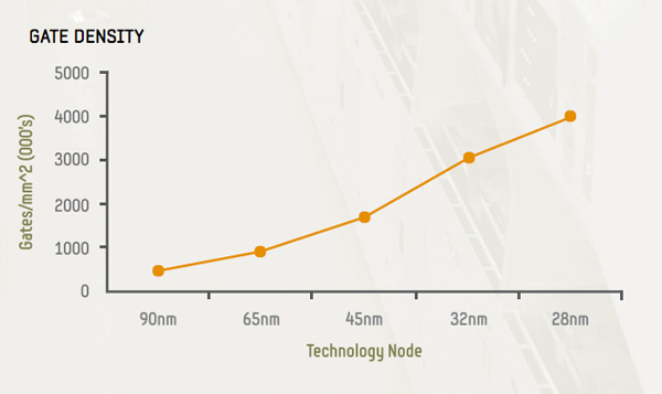
Gate density vs. process node at Samsung

There's another motivation for Apple however. Just as with any good microprocessor company, its best to introduce a new process technology on a known architecture. It's also a good idea to introduce a new process technology on lower volume products. The combination of both of these minimize risk. Should there be something wrong with the new process, introducing a new architecture on it just means you now have two very complex things to debug - the process technology and the chip's architecture. Should the new process not yield very well initially, you'd be similarly screwed if you were depending on it for your highest volume parts.
32nm A5 in iPad 2,4 (Source: Chipworks)


Apple decided to try out Samsung's 32nm HK+MG process on the A5 used in the 3rd generation Apple TV and some of the new iPad 2s. The former is a relatively low volume product for Apple, while the latter still moves in significant quantities. To deal with that fact, Apple is continuing to ship the original 45nm iPad 2,1 alongside the new 32nm iPad 2,4. Any hiccups in Samsung's production of the A5 and there are still more than enough iPad 2,1s to go around. The risk of moving to 32nm is effectively mitigated, while the learnings Apple gains from building the 32nm A5 will pay off later this year as Apple ramps up production of a 32nm SoC for use in the next iPhone. It's a very smart strategy, one you would expect from an experienced chip company - not a device vendor. When you consider that Apple employs chip architects who have worked on everything from the Athlon 64 to the Cortex A15, Apple's behavior is no longer that surprising.


Apple gets two benefits from the iPad 2,4: lower manufacturing costs, and experience with Samsung's 32nm HK+MG process which it will later use in much greater volumes. What about customers who end up with an iPad 2,4? Better battery life and cooler operation, of course.


Impact of HK+MG at Samsung


Remember the basics of Samsung's 32nm HK+MG process: a 40% performance improvement at the same leakage, or a 10x reduction in leakage at the same switching speed. As the iPad 2,4 retains the same clocks as the initial iPad 2, the benefit realized is a significant reduction in leakage current. This translates to tangibly better battery life.


Significant Battery Life Improvements details at http://www.anandtech.com/show/5789/the-ipad-24-review-32nm-a5-tested/2
.....

Final Words

If Apple's A5 is any indication, Samsung's 32nm HK+MG process is extremely capable. Assuming Apple didn't change any fundamentals of its microarchitecture, the iPad 2,4's gains in battery life can be attributed directly to the process. The gains themselves are significant. We measured a 15% increase in our web browsing battery life, a nearly 30% increase in gaming battery life and an 18% increase in video playback battery life. Although Apple hasn't revised its battery life specs, the iPad 2,4 definitely lasts longer on a single charge than the original iPad 2.


If you're in the market for an iPad 2, the 2,4 is clearly the one to get - if you can find one that is. Unfortunately there's no sure fire way to tell that you're getting a 2,4 without opening the box and turning on the tablet, and I suspect most stores will get a bit irate if you're constantly buying and returning iPad 2s in search for a 32nm model. Presumably over time more of the available inventory will shift to 2,4 models, but based on our experiences in trying to find a 2,4 it's still pretty tough.


I would like to applaud Apple's 32nm migration plan. By starting with lower volume products and even then, only on a portion of the iPad 2s available on the market, Apple maintains a low profile and gets great experience with Samsung's 32nm HK+MG process. It's very clear that this is all in preparation for the next iPhone, which will almost certainly use Samsung's 32nm process and require it in significant volumes. It's obvious that Apple employs some very smart chip heads in Cupertino.


What I'd really like to see is a 32nm version of the A5X used in the new iPad. I don't know that there's much reason for that this year, especially when the 4th generation iPad will likely ship in the first half of 2013 with yet another new SoC (dual-core A15 + Rogue anyone?), but it'd still be nice to have. The power efficiency improvements are substantial and the 3rd gen iPad could definitely use them. Those of you who are waiting for the next iPhone should also be pretty happy about these results. Apple could easily deliver a higher clocked version of the A5 for the next iPhone while keeping power consumption equal to if not lower than where it's at today. The move to 32nm is going to be good all around it seems, and Samsung appears to be a very capable foundry partner for Apple. Despite all of the rumors of a rift in the relationship, the foundry side of things is working out well.