Showing posts with label dielectric. Show all posts

Monday, April 6, 2015

3D Semi. Manufacturing Will Benefit LAM, Applied and Other Semiconductor Equipment Vendors

3D semiconductor chip process demand will have a very large impact on semiconductor equipment vendors over the next several years. Initially it is being implemented only on NAND flash

3D chip manufacturing will be implemented by many other types of semiconductor chips such as DRAM memories and other high density ICs.

Historically chip size has been shrinking by using stringent photolithography processes. 3D chip manufacturing enables shrinking chip size while using more relaxed photolithography processes,

3D chip manufacturing relaxes photolithography, but it adds stringent demands on other semiconductor manufacturing processes such as layers deposition and etch. This will increase the demand for equipment vendors such as Applied Materials and LAM as is discussed in the article below.

More about 3D semiconductor from November 2012 is in-  3D NAND flash is coming


More about the processing difficulties is in Applied Materials talks about 3D NAND flash production .

A 2009 patent application by Samsung for this technology is - US20100155810


Ron
Insightful, timely, and accurate semiconductor consulting.
Semiconductor information and news at - http://www.maltiel-consulting.com/


By Tiernan Ray
Credit Suisse’s chip equipment analyst Farhan Ahmad and chip analyst John Pitzer today write that equipment vendors Lam Research (LRCX) and Applied Materials (AMAT) could both see multiplication of their sales as a result of newer three-dimensional NAND flash memory chips, known as “3-D NAND,” that are becoming more prevalent.
Why are the chips important? 3-D NAND chips have 35% more bits per square millimeter, the authors write, at least in the parts produced by Samsung Electronics (005930KS). With increasing “layers,” that can rise to more than double and perhaps triple the bit density.
As a result of density rising faster than costs, “As the density growth is significantly higher from 2D to 3D, than the CapEx increase from 15nm to 3D, we believe that 3D NAND roadmap can potentially provide a 20%/yr cost reductions for next two years.”
While 3-D NAND has been talked about for some time, the key is that the prices of the products are declining rapidly in the marketplace, as evidenced by Samsung’ ssolid-state drives using the chips, the authors write:
We would note the following recent data points (i) Samsung 3D NAND SSD pricing is now at parity with Planar SSDs. Retail pricing indicates that Samsung’s 3D NAND SSDs have declined 20-25% qtd and are now on price parity with leading planar SSDs. Note that 3D NAND SSD are known to have better reliability relative to 2D NAND SSDs, which makes 3D NAND SSD as better choice at same price points. We believe that recent price reductions are a sign that Samsung is trying to accelerate the adoption of 3D NAND and this could prompt other NAND companies to accelerate adoption of 3D NAND. (ii) SanDisk and Micron 3D NAND announcements are indication that 3D NAND progress is not just limited to Samsung, and there is greater evidence that 3D NAND can significantly reduce cost on NAND (our analysis suggests that 48/64 layer 3D NAND could offer >20% cost reduction over planar). Note that once 3D NAND becomes more economical relative to planar, transition to 3D could accelerate as NAND Companies try to compete on costs. (iii) We are seeing more signs of product wins for 3D NAND. Earlier today Korea Times reported that Samsung’s 3D NAND SSD had secured design wins at GOOG and AMZN data centers. Earlier this month Korea times had also reported that Samsung’s 3D NAND had won the Apple’s MacBook business for next year.
For Lam and Applied, they write,
Our analysis suggests that 3D NAND transition could potentially increase NAND WFE to $9-12bn /year for 2016-2018 versus $5-6bn over last 2 years (assuming 40% bit growth per year). We believe that NAND revenues for LRCX could potentially increase by 3x (or $1.5 bn per year) as 3D NAND accelerates. We also expect AMAT to benefit from the 3D NAND transition but estimate that NAND revenues for ASML will decline by > 50% as litho intensive CapEx for planar NAND is replaced by non litho intensive CapEx for 3D NAND.

Monday, March 24, 2014

Apple 64 bits,Mobile DRAM Market, and Masking Lithography


"mass producing what the company said is the most advanced 4Gb DDR3 memory based on a new 20 nanometer process technology using immersion ArF lithography...

key element of the new design and manufacturing technology is a modified double patterning and atomic layer deposition that allows for continued scaling. The new approach to double patterning enables 20nm DDR3 production using current photolithography equipment, Kadivar said. “We have found the most efficient way to manufacture high density DDR3 technology, in this case 4Gb.” Samsung has also created ultrathin dielectric layers of cell capacitors with a very high level of uniformity, which is an important contributor to higher cell performance."

While in the ecosystem of mobile DRAM products sale and marketing -

 “After the 64bit AP was first applied to the iPhone 5S by Apple last year, it was expected to become the basic performance of premium smartphones. However, companies in the Android camp cannot bring themselves to use the 64bit AP. The 64bit AP is not compatible with the Google Android OS yet…

Qualcomm has already unveiled the 64bit Snapdragon, and SEC is known to have almost developed the 64bit AP. If the OS problem is solved, it appears that Android smartphones will not have much difficulty adopting the 64bit AP.

The delayed commercialization of the 64bit mobile AP impacted on the DRAM market. 1~2GB mobile DRAMs are used in 32bit AP smartphones, but 64bit AP smartphones come with 3GB or bigger DRAMs. Memory semiconductor makers established the mobile DRAM production plan for this year in consideration of the demands for the 64bit AP. As demands are not picking up, the Q2 contract prices of mobile DRAMs are expected to go down. (http://english.etnews.com/device/2933349_1304.html)


Ron
Insightful, timely, and accurate semiconductor consulting.
Semiconductor information and news at - http://www.maltiel-consulting.com/


Korea's DRAM Market Suffers as Google Delays Android 64-bit


Apple introduced the first smartphone in the world to run on a 64 bit architecture last September. The iPhone 5S lead the way. Thereafter it was simply expected to become the basic performance of premium smartphones. However, Android OEMs can't match Apple's offering because Android isn't 64bit compatible at the moment even though Qualcomm has a 64bit processor ready to ship. While Samsung is hoping to be the first Android OEM to deliver a 64bit based smartphone this fall, industry Insiders aren't so sure it'll be ready in time. In fact they believe that will be pushed into sometime in 2015.


Those in the DRAM market have suffered a direct blow due to Google's inability to deliver a 64bit version of Android. 

Friday, May 3, 2013

Samsung NAND 1xnm Manufacturing TLC (Triple Level)

The article below discuss leading edge process and cell technology of 20 nm flash NAND cell.

"Samsung's 21 nm NAND flash device is fabricated using a triple metal, double poly, 21-nm CMOS process. The single transistor flash cell measures approximately 42 nm by 46 nm for a physical cell area of 0.0019 µm2.  Its  competitors  in  process technology include  a 19-nm, 32-Gbit  MLC  NAND  flash from Toshiba and   a  20 nm 32 Gbit MLC NAND Flash from Intel-Micron."

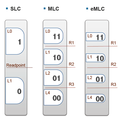
SLC, MLC & eMLCSee Intel 20nm process  technology from March 2012 Micron/ Intel 20-nm 64G MLC NAND Flash Memory Reverse Engineered

3D is likely to be a strong contender for scaling leading edge NAND flash.

See Samsung Advances Memory Storage eMMC to 1x-nm Process regarding what 10 nm really is.

Ron
Insightful, timely, and accurate semiconductor consulting.Semiconductor information and news at - www.maltiel-consulting.com


Samsung hits triple-level-cell NAND flash milestone

Arabinda Das, 5/1/2013 1:32 PM EDT

http://www.eetimes.com/design/memory-design/4413213/Samsung-hits-triple-level-cell-NAND-flash-milestone?pageNumber=0&goback=%2Egde_1803012_member_237577215


Samsung announced recently that it started production of advanced NAND flash devices with 128Gbit, triple-level cell (TLC) NAND memory using 10-nm class process technology.

Similarly, Micron also announced in February that it would come to market with NAND flash devices with a memory capacity of 128 Gbit that also use TLC design. It was only last fall that Samsung introduced a 64 Gbit NAND flash using TLC and 21-nm process technology.

Clearly, the industry is moving toward TLC cell design even for demanding SSD applications. The concept of a multi-bit per cell technology was first introduced by Toshiba and for the last five years, all flash device makers have products using the 2-bit per cell design. (Download TechInsights' flash NAND technology roadmap here).

A multi-bit cell device has a high density and a low cost per bit, but usually has a reduced endurance. In a conventional single bit flash device the number of electrons placed on the floating gate affects the threshold voltage (Vt) of the cell. This effect is used to set the state of the cell to either high or low.

In a multi-bit cell the threshold is set to several different values. The difference in voltage between these levels is small, which puts an additional constraint of placing the charge precisely on the floating gate and of sensing it correctly. In a 2 bit per cell memory, the cell is put in four states. In a 3-bit per cell there are eight states (states = 2n), which imposes a colossal task for flash device manufactures to have a tight cell threshold voltage distribution and a precise sensing of cell data.

According to several papers, the number of electrons stored on a floating gate for the 30-nm node class is slightly less than 100. So, in a 21-nm node with the TLC design, the circuitry for placing and sensing charge on the floating gate is dealing with only a few tens of electrons in each state.

Therefore, Samsung’s 21-nm, 64 Gbit TLC NAND flash can be considered an industry milestone. It is the first commercial SSD product using the TLC design in 21 nm node. TechInsights has done a structural analysis of the 21-nm, 64 Gbit TLC NAND flash and is also following up with a waveform analysis.

The K9CFGY8U5A-CCK0  21-nm flash memory  is one of the industry’s leading flash memory devices, packing 64G bits into a single 102.87 mm2 die, using conventional floating-gate flash memory technology. This NAND flash was found in Samsung’s latest SSD drive, the SSD840 (256GB). The basic teardown of the SSD drive is shown in figure 1.

Samsung's 21 nm NAND flash device is fabricated using a triple metal, double poly, 21-nm CMOS process. The single transistor flash cell measures approximately 42 nm by 46 nm for a physical cell area of 0.0019 µm2.  Its  competitors  in  process technology include  a 19-nm, 32-Gbit  MLC  NAND  flash from Toshiba and   a  20 nm 32 Gbit MLC NAND Flash from Intel-Micron.

Floating gate technology.
All NAND flash memories continue to evolve the floating gate technology. But the basic cell structure has remained unchanged throughout several process generations. The self-aligned floating gate poly (SAP) process is still used by the three major manufactures.

Intra-gate poly to poly contacts are adopted by all manufacturers. In fact, two of the major manufacturers are still using the control gate (CG) and inter-poly dielectric (IPD) wrap around the floating gate (FG) configuration. Managing to keep most of the processes steps the same as the previous node is a great advantage for manufacturing because all the accumulated experience in process development is utilized to produce the new generation of devices. And yet every new node is a technological feat.

With every new technology node, the memory density (Mbits/mm2) increases and the process technology becomes more complex because all features on the die shrink but do not shrink proportionately with the same ratio.

Figure 2, shows a compound picture where the top image is the SEM cross-section along the Bitline direction of Samsung 21-nm TLC NAND flash and the bottom image is the corresponding topographical image at poly Wordline level. Figure 2 shows that the NAND string is consisting of 64 active Wordlines, two dummy Wordlines two select transistors at both end of the Wordlines and two contacts (Sourceline and Bitline).


Figure 2: Correlating SEM cross-section in Bitline direction with topographical image at poly-Wordline level. The topographical image shows the staggered Bitline contact layout.

The ratio of the length of the active Wordlines to the NAND string length is the overhead factor. Table 1 recapitulates some of the important features of last three Samsung NAND flash devices. This table puts in evidence the fact that the active cells are shrinking more than the string-select and ground select transistors and as a consequence the NAND string overhead has been increasing for the last three generations. As the active cells shrink the close distance between adjacent floating gates leads to parasitic capacitance which may  result in a Vt shift. Samsung has done a major process change in 21-nm NAND flash devices to counter the parasitic capacitance issue as elaborated in Figure 3.


Table 1: Compiling some of the NAND cell features of last three Samsung NAND flashdevices. TLC designs make a huge impact on the memory density. As the technology scales down, the overhead seems to increase.Figure 1: Basic teardown, from SSD 840 drive to single NAND flash die.

Tungsten metal gate.
This 21-nm NAND flash has abandoned the silicide process and opted for tungsten metal gate. This transition is not new; it has already been done in many DRAM products. However, depositing tungsten on poly is not a straightforward process; several interface treatments have to be done, which are described in the report.

Tungsten metal gates leads to controllable air gaps, which mitigate the parasitic capacitance. Other challenges including choosing a suitable inter-poly-dielectric (IPD) layer. The IPD thickness affects program/erase speed and magnitude of read current and the quality of the dielectric layers has a direct impact on the endurance of the flash device. 

A thinner of IPD layer will increase the capacitive coupling between the control gate (CG) and the floating gate (FG) and generate a higher read current and a faster program erase mechanism but can also compromise the retention capability. So a tradeoff has to be made.

The IPD layer composition in 21-nm NAND flash is still the same as the previous generation but the individual layer thicknesses are modified. Also, in the Wordline direction, the aspect ratio for poly 2 gap-fill is greater than five. Here, too, Samsung has come up with new process techniques. Samsung’s 21-nm 64 Gbit TLC NAND flash technology has a process flow similar to its previous generation but with an enhanced process capability. It remains to be seen if the next generation 10-nm class 128-Gbits TLC NAND flash will manage to prolong the existing process flow or will take the next big step of fabricating 3-D NAND stacks.

Interested in NAND flash technology? You can check out TechInsights' technology roadmap for NAND flash here.

Arabinda Das is a senior process analyst at TechInsights.

Wednesday, January 30, 2013

Where is DRAM Innovation?


The article, Hynix 30 nm DRAM layout, process integration adapt to change ,  discusses advances in DRAM memory at Hynix. DRAM memory has not been able to shrink the memory cell as quickly as flash memory. Leading edge flash memory products with dimensions around 20nm or less are being introduced to production, while DRAM memory is still above 30nm (see figure 4 in the article below).


While flash memory has a key advantage of keeping the information even without power, there is still a place for DRAM memory. Many of the process technology advances are being implemented at a slower rate in DRAM production. However major memory cell and circuit improvements are not being pursued. For example, storing multiple bites in one physical flash memory cell has been done for several years. There are 3-bit-per-cell (TLC) NAND and 2-bit-per-cell (MLC) flash available in the market, but there is no DRAM product with multiple bits in the same cell.

Ron

Insightful, timely, and accurate semiconductor consulting.
Semiconductor information and news at - http://www.maltiel-consulting.com/


Tuesday, January 22, 2013

MLC Flash Memory New Future

A new development by Macronix has the potential of extending flash NAND memory technology for several additional generations.


In 2012 IEDM conference Macronix engineers presented a paper on radically improving flash memory program /erase cycling endurance to more than 100 million cycles by localized heat treatment .  Currently, most advance flash NAND products are limited to less than 100,000 cycles. The larger memory devices, called MLC flash, can store 2 or 3 bits in each memory cell. However, their cycling endurance is limited to less than 10,000 cycles. The new heating method will increase the cycling endurance of MLC flash. An improved cycling endurance would enable development of higher density MLC flash cells with larger numbers of bits per cell.

Macronix's new heat treatment that heals the memory cell can impact other layers in the memory cell. For example, it can change electromigration properties of metal lines nearby. It can also produce mechanical stress around the heat spots. The impact of the heat treatment has to be optimized, since the potential of creating larger flash memory looks promising. Already Macronix will present a flash memory chip with 6 bits per cell at the 2013 ISSCC.


Ron

Insightful, timely, and accurate semiconductor consulting.
Semiconductor information and news at - http://www.maltiel-consulting.com/


Monday, January 7, 2013

3D Flash Memory Marching Forward

3-D Flash starts to appear in the market. Hynix version is based on VSAT technology.


See more about VSAT at http://www.maltiel-consulting.com/3D_Charge_Trapping-CT_NAND_Flash.pdf .


The dramatic iincrease in flash memory cycling endurance (mentioned in IEDM 2012) is likely to extend the life of the basic flash NAND technology.


Ron
Insightful, timely, and accurate semiconductor consulting.
Semiconductor information and news at - http://www.maltiel-consulting.com/


Hynix to start sampling 3D flash memory chips

04 Jan 2013

South Korean memory semiconductor supplier SK Hynix said earlier this week that it would begin mass production and sampling of 3D flash memory chips that utilises vertical-stacked-array-transistor (VSAT) technology, according to a report by the Korea Times.

Flash chip, which is a type of non-volatile memory that can be erased and reprogrammed, is ideal for data-intensive devices that constantly connect to the Internet. It has a simple cell structure that allows for higher memory capacity, density and durability.
"As far as I know, all major semiconductor companies are investing more in the development of 3D flash memory chips. SK Hynix is trying hard to mass produce them as early as possible," said CTO Park Sung-wook. Samsung Electronics is reportedly planning to produce 3D flash memory chips in its plant in Xi'an, China upon completion of the facility.

Wednesday, March 28, 2012

Micron/ Intel 20-nm 64G MLC NAND Flash Memory Reverse Engineered

Intel and Micron’s joint venture for process development, IM Flash Technologies (IMFT), has successfully developed and manufactured high density multi-level NAND flash memories with a 20-nm design rule for the first time. IMFT also revealed a fully planar floating gate cell design.


IMFT has introduced a cell planarization integrating with high-k/metal gate (HKMG) stack.For a new cell structure, oxide-nitride-oxide (ONO) inter-gate dielectric layer is replaced by a stack of high-k dielectrics to restore the FG to CG coupling ratio. Thinner polysilicon floating gate technology is likely adopted to lower the cell-to-cell interference.


An air gap isolation process is adopted to reduce capacitance coupling between cells (more below).


Ron Maltiel


Delving deep into Micron and Intel’s 20-nm 64-Gbit MLC NAND flash memory

http://www.eetimes.com/electronics-blogs/other/4369862/Delving-deep-into-Micron-and-Intel-s-20-nm-64-Gbit-MLC-NAND-flash-memory?pageNumber=0
Young-Min Kwon,                                                                      3/26/2012 7:38 PM EDT

UBM TechInsights recently analyzed IMFT's 20-nm, 64-Gbit MLC NAND to get a better understanding of the advanced process technologies and innovative cell architecture. The success of NAND flash memory in the semiconductor market is mainly driven by continuous and tremendous growth in the mobile phone and tablet PC markets, and the growth of adoption of high performance solid state drives (SSDs) as a replacement for hard drives in computers. As Intel and Micron jointly announced last year, a NAND flash product with a terabit capacity, comprising a simple stack of several dice, can be realized with the advent of 20-nm manufacturing technology in conjunction with a break-through concept in cell architecture.

During the past years, NAND flash has enjoyed the highest density among the commercial memories due to its excellent physical scalability and multi-level cell (MLC) approach with two or three bits per cell. However, the recent demand spike for NAND flash memories in portable electronics has resulted in a much drastic scaling down of the device structure of NAND to obtain higher density, faster speed and lower bit cost devices. The aggressive scaling of a cell size in NAND flash memory is expected to face severe barriers in sub-20-nm floating gate-based flash cell with conventional architecture.

In response to the challenges mentioned, Intel and Micron’s joint venture for process development, IM Flash Technologies (IMFT), aggressively pursued a NAND cell shrink, and, as a result, has successfully developed and manufactured high density multi-level NAND flash memories with a 20-nm design rule for the first time. IMFT also revealed an innovative memory structure with the introduction of a fully planar floating gate cell design. IMFT, often considered a leader in the NAND flash manufacturing process, has introduced a cell planarization integrating with high-k/metal gate (HKMG) stack that would considerably overcome many of the physical and electrical scaling challenges brought on by moving to the 20-nm node or further beyond.

UBM TechInsights recently analyzed IMFT's 20-nm 64Gbit MLC NAND to get a better understanding of the advanced process technologies and innovative cell architecture.

By introducing the 20-nm process technology in the production of their 64-Gbit MLCNAND flash memory, IMFT establishes itself as the leader in new process node implementation. Measuring in with a die size of just 117 mm2, this NAND device features an area size that is approximately a 30 percent reduction over the IMFT’s existing 25-nm 64-Gbit NAND flash. IMFT’s 64-Gbit NAND flash is fabricated in a single poly, metal gate and triple metal levels and is distributed in a 48-pin lead-free TSOP package. The 64-Gbit of single flash memory die is divided into four banks with one-sided bond pad arrangement and memory area efficiency is 52% which is comparable to previous 25-nm 64-Gbit NAND device having the die size of 162 mm2.


In a conventional NAND floating gate cell, the control gate (CG) and inter-poly dielectric wrap around the floating gate (FG) and coupling factor greatly relies on the floating gate sidewalls as shown in the figure below.


Conventional floating gate NAND (IMFT’s 25 nm NAND flash)


Delving deeper

For the 20-nm and below technology node, the cell spacing is already too narrow to allow a control gate plug between the floating gates. As a result, the NAND flash memory will have to adopt a planar cell configuration by eliminating the control gate-floating gate wraparound.

Charge trapping-based flash (CTF) memory had been considered as an alternative, with CTF having a planar cell structure, but unfortunately we have yet to see a successful debut in NAND production quite yet. With all these factors at play, metal as control gate in combination with a stack of high-k inter-gate dielectrics (IGD) above thinner floating gate would be the potential solution to continue the scaling of NAND flash beyond the 20-nm node with existing floating gate-based NAND flash technology.


Planar floating gate NAND (IMFT’s 20-nm NAND flash)

Key technologies in the process and new flash cell structure

IMFT's 20-nm technology with a fully planar cell structure and key process advances have overcome several critical problems of conventional floating gate cell architectures in such a small flash device:

• Control gate (CG) poly-Si filling to narrower space between adjacent floating gates

• Cell-to-cell interference

• Scaling limitation of inter-poly dielectric (IPD) and smaller CG to FG coupling ratio.

In order to manufacture a 20-nm NAND cell, advanced cell pitch reduction techniques (such as double patterning technology) are used for critical lithographic steps. To pattern below the 20-nm design rule, quad patterning technology will also have to be implemented to overcome the limitation of 193 nm ArF immersion double patterning. This, however, could be still a ways away as the extreme ultraviolet lithography (EUV) tool required to address this patterning issue is still too expensive for flash memory production. For this NAND component, a single flash cell measures around 40-nm in both the wordline and the bitline direction yielding a physical cell area of 0.0017 µm2. That makes this cell most likely the smallest cell in NAND production. A planar floating gate structure has been implemented in this NAND device, in conjunction with thin polysilicon floating gate, a stack of high-k inter-gate dielectrics (IGD), and metal control gate.

For a new cell structure, oxide-nitride-oxide (ONO) inter-gate dielectric layer is replaced by a stack of high-k dielectrics to restore the FG to CG coupling ratio which should be reduced in planar cell structure. Thinner polysilicon floating gate technology is likely adopted to lower the cell-to-cell interference. A metal gate-based wordline is defined by etching the multiple gate stacks using the hard mask layer. As the cell pitch is aggressively scaled, the increased capacitance coupling between cells is a severe issue, since increased cell-to-cell interference leads to cell performance degradation and reliability problem. In order to overcome these problems, an air gap isolation process is adopted for both cell gates and metal 1 bitlines. An air gap structure has been reported to act as a low dielectric constant gap filling materials. The bitline contacts are formed as a staggered layout to obtain better lithographic margin, and a NAND string has 68 wordlines.

New cell architecture combined with key integration technologies observed from IMFT’s 20-nm MLC NAND flash is very promising to further extend the life span of conventional floating gate flash memory with more aggressive cell scaling. However, with a further reduced geometry of floating gate, the electrons captured will be drastically decreased, which could result in the need to manage less than 20 electrons in 1x-nm MLC NAND flash. That’s why novel device concepts or alternative memory solutions, such as those found in IMFT’s latest NAND flash device, reveal a preparedness to replace NAND flash memory in near future since scaling demand and reliability challenges will be much higher in dominant mobile applications. For example, the CTF seen in this NAND coupled with 3-D configuration could be seen as a viable near-term alternative to current planar NAND flash technology while a large variety of new memory concepts are emerging and competing for the replacement of NAND flash memory. Floating gate NAND flash will eventually arrive at its scaling limit but it’s not quite hitting the wall just yet. It will be very interesting to see what changes IMFT, and other flash manufacturers, incorporate to overcome these scaling limitations in the future.

Thursday, March 15, 2012

Is Resistive RAM (RRAM) The Future Flash Memory?


Below is an overview of Resistive RAM (RRAM) by Bogdan Govoreanu, from IMEC . This new flash memory technolgy is worth watching.


Eli Harrari, Sandisk founder, CEO, and Chairman from its founding until January 2011 in his ISSCC Plenary talk stated that 3D-RRAM " has a real shot at becoming the next big game-changer in the second half of this decade".

Eli Harrari foresaw upcoming changes in non volatile memory. He converted Sandisk from supporting both NOR and NAND flash to only NAND long before other companies saw the upcoming accelerating growth in NAND.

Ron Maltiel


Resistive RAM for next-generation nonvolatile memory
Bogdan Govoreanu, imec Leuven                                               3/12/2012 1:25 PM EDT


Since its introduction in 1988 by Toshiba1, NAND flash nonvolatile memory has undergone an unprecedented growth, becoming one of today’s technology drivers. Although NAND flash memory has scaled to 1x-nm feature sizes, shrinking cell sizes reduce the number of electrons stored on the floating gate. Resistive RAM (RRAM) provides an alternative. In this article, we review the main performance figures of hafnium-oxide (HfO2)-based RRAM cells4 from a scalability perspective, outlining their strengths as well as the main challenges ahead.

A NAND flash nonvolatile memory cell, usually a floating gate transistor, implements the memory function by charge stored on the floating gate. With a charge transfer mechanism onto/from the storage medium that relies on tunneling and a serial (string) architecture, NAND memory features high operating voltages (with associated chip area consumption for the on-chip voltage generation), rather long cell program/erase (P/E) times, and slow read-access times. These drawbacks are, however, compensated for by the very compact array architecture and extremely low energy-consumption-per-bit operation, which eventually enabled fabrication of high-density memory arrays, at low cost and with a chip storage capacity increasing impressively.
During its extraordinary evolution, NAND flash has often met seemingly insurmountable barriers. Technological, architectural, and design innovations complemented each other, however, enabling continued scaling. Nowadays, NAND flash memory seems to have found the way toward the realm of 1x-nm feature size, with major players fighting for each nanometer of cell shrinkage, not to mention for supremacy. Nevertheless, the scaling of cell size leads to gradual reduction of the number of electrons stored on the floating gate, with a projected number of less than 30 electrons for memorizing a (multilevel) cell state, for an assumed 15-nm feature size2.

Resistive RAM (RRAM), just like phase-change memory (PCM), is emerging as a disruptive memory technology, implementing memory function in a resistance (rather than stored charge), the value of which can be changed by switching between a low and a high level. Although the phenomenon of reversible resistance switching has been since the 1960s, recent extensive research in the field has led to the proposition of several concepts and mechanisms through which this reversible change of the resistance state is possible. The distinctive feature of most RRAM concepts3 consists of the localized, filamentary nature of a conductive path formed in an insulating material separating two electrodes (a metal-insulator-metal (MIM) structure), corresponding to the on-, low-resistance state. This attribute was immediately associated with a high scalability potential, beyond the limits currently predicted for flash memory.

Resistive memory structures

Even if many materials reported to date exhibit good resistive switching properties, the success of a future RRAM technology is critically dependent on the ability to integrate these materials/switching structures into a conventional, supporting baseline technology, with cost as a key success factor. Not surprisingly, fab-friendly and accessible materials such as HfO2, zirconium dioxide, titanium dioxide, tantalum dioxide/ditantalum pentoxide, etc, which showed resistive switching behavior, have received the highest attention.

A thin HfO2 dielectric film sandwiched between two metal electrodes was shown to have resistive switching properties, either uni- or bipolar, depending on the materials used as electrodes and on the method to deposit the active (oxide) film. The bipolar operation of HfO2, requiring voltages of opposite polarity to switch on/off the cell, is believed to be due to the formation of conductive paths (filaments) associated with presence of oxygen vacancies (VO), which can be ruptured/restored through oxygen/VO migration under electric field and/or locally enhanced diffusion. The bipolar operation of HfO2 is preferred for its increased immunity to disturbs and over reset. The formation of the filament (forming, or electroforming) is believed to take place along pre-existing weak spots in the oxide, for instance along the grain boundaries in case of a polycrystalline HfO2, which presumably have larger amount of defects and also a higher oxygen diffusivity compared to the bulk of the material.5,6

An alternative approach is to use a metal/oxide material system7 with a reactive (capping) metal, capable of chemically reducing the HfO2. Although a Hf/HfO2 system may seem an obvious choice, selection of hafnium as a cap layer is supported by thermodynamic considerations that indicate a low oxide formation energy, when reducing HfO2. A similar property is found for the titanium/HfO2 case. In the Hf/HfO2 system, hafnium acts as an oxygen buffer layer that allows, under electrical stimuli, the production of oxygen-deficient off-stoichiometric oxide, thus favoring formation of the switching filament. Furthermore, conventional physical vapor deposition (PVD) titanium nitride was used to define the bottom and top electrodes (BE/TE) in a crossbar-patterned configuration.

To achieve best flexibility and controllability of RRAM device operation, the resistive memory structure was connected serially with an nMOS transistor, which acts as a cell selector. Figure 1a shows a top view scanning-electron-microscopy (SEM) picture of a test structure, while high-resolution transmission-electron-microscopy (TEM) cross-sections of the structure along the main directions, visualizing the BE/TE are shown in figure 1b and figure 1c. The smallest fully functional working structures processed4, feature an effective area of around 10 x 10 nm2, defined by the BE width and by the width of the TE/Hf-cap tip resulting after the crossbar patterning.


Figure 1: Top SEM-view of a crossbar resistive element (a) and high-resolution TEM cross-sections of the bottom- (b) and top-electrode (c).


The oxide thickness is the main parameter determining the value of the forming voltage (VF), which is typically the highest voltage and needed only once, to get the RRAM cells ready for operation. In contrast, the Set (on-switching) and Reset (off-switching) voltages are lower and, in a common situation, do not depend on oxide thickness. This difference makes it possible that VF can be then reduced by thinning the oxide layer, without interfering with normal cell operation. Furthermore, aggressive oxide thinning may eventually lead to forming-free operation.

The Set/Reset (S/R) voltages, as well as the levels of the on/off states, turn out to be essentially independent not only of oxide thickness, but also of cell size. Although operating the cell in extreme conditions (i.e. with very deep Reset or strong Set switching) may turn these characteristics invalid, the common situation is consistent with the filamentary nature of the conductive path; furthermore, it supports the model of a partial rupture and restoration of the filament during device operation. Eventually, the oxide thickness corresponding to forming-free operation, confirmed experimentally to be in the range of 2 to 2.5 nm, is indicative of the extent of the ruptured portion of the conductive filament.


Electrical performance and reliability

Given the structure asymmetry induced by the presence of the hafnium layer, the RRAM cells are best operated in bipolar mode with positive polarity on TE for the Set and forming operations and with negative polarity on TE for the Reset operation. In this section, we will discuss the most important performance and reliability figures of the HfO2-based RRAM cells.


Switching speed

To measure switching speed, we used a pulsed operation mode, exemplified here for a Reset switching. Thus, stimuli were applied on the sourceline (SL) and wordline (WL) of the serial 1T1R (1-transistor, 1-resistor) test vehicle, while the response was monitored with a digital oscilloscope on a small series resistance attached to the cell bitline (BL; see figure 2a) . The switching was time-confined to a maximum duration given by the width of the SL pulse, i.e. 10 ns. We carefully designed the experimental setup to minimize the impact of the parasitic elements (e.g. capacitances), having a reasonably short system time constant. The resistive element, initially in the on-state, switches to the off-state quickly, leading to a decrease of the signal within just 3 to 4 ns (see figure 2b). When taking into account the impact of the testing environment on the collected waveform, the observed transition time duration gives a higher margin for the intrinsic switching time, which can be shorter.


Figure 2: Schematics of the device under test (DUT), with applied stimuli and collected response (a) and waveforms corresponding to a Reset switching (b), sampled with a LeCroy WavePro 740Zi 4GHz oscilloscope. The 10-ns SL pulse (blue color), which enables switching, in contained in the longer WL pulse (red color) used to open up the transistor’s channel. The Reset switching is confirmed by the read-out (RO) of the cell current, which changes from high value (on-state) before the SL applied pulse to low value (off-state) after the pulse.


On/off window & operating voltages

The on/off window easily exceeds a factor of 10, with modest (<1 V) voltages applied for both S/R operations. Using higher amplitude pulses and switching verification will improve the on/off window by at least two orders of magnitude, as well as enhancing the uniformity of the switching operations (see figure 3a), which may open up paths for multilevel operation.


Figure 3: Typical on/off window (expressed in read-out cell current) achievable with sub-3-V pulsed operation, with verify (a) and Reset pulse amplitude-duration voltage-time trade-off, showing no significant degradation when scaling cell size from 1 um2 down to 10 x 10 nm2 (b). Data are for an oxide film thickness of 10 nm. The dashed lines are guide for the eye. Similar conclusions hold for Set switching (not shown).


The voltage-time dilemma is a popular term used to express the limited ability of RRAM to display nonlinearity. This is however not specific to RRAM, but present in virtually all memory structures, which ideally need to on one hand allow for indefinitely long stability under no or low-electrical stimuli (for retention, read-out and disturbs immunity), while on the other hand providing fast change of state under operating stimuli (for P/E or S/R).

The S/R voltages required to operate these cells thus display the usual trade-off with time. Nevertheless, the pulse amplitude-time dependence shows that the cells can still be operated with voltages well below 3 V, even for pulses as short as 10 ns. Furthermore, in a comparison of large area cells (in the order of 1 um2) with smallest-size cells (of 10 x 10 nm2), the voltage-time characteristics maintain similarity (see figure 3b), which shows that we should expect no considerable performance degradation when considering aggressively scaled structures. Compared to NAND flash, RRAM has the benefits of low-operating voltages.


Reliability: retention & endurance

The usual 10 year requirement for NVM retention is met by most of the RRAM cells, with a median cell reaching this limit at an extrapolated temperature of around 100°C. As expected, retention turns out to be most critical for the on-state, where retention loss is attributed to filament dissolution. Retention improvement is possible through material optimization and careful sealing of the active region with oxygen-free layers.

Endurance tests performed on unoptimized samples showed cycling of at least 10 Mcycles in a single shot. The failure at the end of the tests was, however, recoverable with a stronger stimulus to “unlock” them from the stuck state, and cycled again with adjusted slightly stronger conditions. These facts suggest that careful balancing of the S/R test conditions, next to process improvement, may allow superior reliability and extended device lifetime, which can well exceed billion cycles, even on the smallest device sizes. This figure is far above the conventional requirement for flash memory, pinpointed to 100 kcycles, although reference value for data storage flash is commonly lowered down 10 kcycles, on arguments of practical, as well as economical nature associated with a commodity product.

Scalability, energy consumption, and cell array considerations

The data discussed so far provide evidence of RRAM operation on an effective area of nearly 10-x-10-nm2 without compromising any of the major performance or reliability figures. This size is the smallest reported to date, for HfO2-based RRAM cells and demonstrate cell scalability in the nanometer range, which is beyond scaling limits of NAND flash. Filament formation has been observed experimentally, for instance on TEM pictures, for metallic filaments, such as those formed in nitrous oxide RRAM.


Figure 4: Extracted filament size for 10-x-10-nm2 cells, operated with 10-ns pulse duration. The filament was asssumed cylindrical, with a saturated sub-stochiometric hafnia resistivity.8


In the cells under discussion here, conductive paths presumably formed by oxygen vacancies corresponding to locally lower fractions of oxygen content in the active oxide layer are hard to detect, due to resolution limits of the physical characterization methods. Oxygen-deficient HfO2, however, has a resistivity that correlates with the amount of oxygen-deficiency, but eventually saturates for highly deficient stable sub-oxides, at a value still significantly higher than that of metallic Hf.8 When combined with experimental electrical data corresponding to on-state (measured on the smallest 10 x 10 nm2 HfO2-based RRAM cells), this property allowed extracting the radius of an assumed-cylindrical filament, with a median value of nearly 1 nm. Although an estimate, this result suggests intrinsic scalability of the resistive memory element in the few-nanometer range.

One of the key features of NAND flash technology is the extremely low power required to write/erase a single cell, as it only involves very low (Fowler-Nordheim) tunneling currents. This translates, in spite of the need to use high P/E voltages, into a low energy used to operate a cell, even with the long specific cell P/E times, thus enabling a high throughput in NAND flash. RRAM, by contrast, works at much lower voltages and on/off switching is several orders of magnitude faster than for NAND cells. The current is, however, significantly larger and even if RRAM scores well in comparison with MRAM9 and PCM technologies10,11 there are concerns about the circuit level implications.


Figure 5: Benchmarking of HfO2-based RRAM in relation with existing (NAND flash) and other emerging technologies (MRAM, PCM). An improvement direction implying use of shorter pulses is identified experimentally.4

When we consider the switching energy per bit operation, RRAM is approaching the performance of NAND flash, given the actual peak current levels during switching as high as a few tens of microamps. Crossing below a 10-fJ-NAND flash border would require nanosecond switching speeds, or sub-microamp switching currents; paths to meeting these requirements are currently pursued.

RRAM has device-level characteristics that meet most of the nonvolatile memory requirements. It furthermore shows scalability potential in an area that is thought to be inaccessible to NAND flash. To be able to exploit these strengths at circuit/system level, RRAM must overcome cell read-out interference12 that may cause in erroneous read out of the (HRS) cell state, due to so-called sneak-current paths. Alleviation of this issue requires a bidirectional selector device. The control transistor in a 1T1R structure provides this functionality and it is, in fact, a potential solution for memory arrays in which density is not the main concern. For data storage applications, however, achieving highest memory density should aim at a cell footprint of around 4F2 (with F being the feature size), implementation of which will, most likely, require the use of a two-terminal selector device13 or a rectification function built into the memory element itself (self-rectifying resistive memory). Research achievements in this direction, complemented by consideration of practical possibilities to increase effective density by using 3D architectures14 for meeting cost effectiveness, will eventually determine the success of RRAM as the future nonvolatile memory of choice.

In summary, HfO2-based RRAM shows great promise for future generation nonvolatile memory, offering a fab-friendly option, with performance characteristics that qualify it for a fast, low-voltage, low-energy-consumption memory, with a good and perfectible reliability, as demonstrated for fully-functional 10-nm-size devices and with inferred intrinsic scalability down to a few-nanometer size. Further improvement in reliability and additional “in-the-footprint” or built-in selection functionality set important milestones ahead on the road to becoming tomorrow’s nonvolatile memory.


Note: This article is based on the work reported at IEDM 2011 by the Emerging Memory Devices Program team of imec Leuven.4


References

1. M. Momodomi et al, IEDM Tech. Dig, pp. 412-415, 1988.

2. K. Prall, Proc. NVSMW, pp. 5-10, 2007.

3. R. Waser, IEDM Tech. Dig, pp. 289-292, 2008.

4. B. Govoreanu et al, IEDM Tech. Dig, pp. 729-732, 2011.

5. G. Bersuker et al, IEDM Tech. Dig, pp. 456-459, 2010.

6. U. Brossmann et al, J.Appl.Phys, 85(11): 7646-7654, 1999.

7. B. Govoreanu et al, Ext. Abstr. SSDM, pp. 1005-1006, 2011.

8. E. Hildebrandt et al, Appl.Phys.Lett, 99: 112902, 2011.

9. K. Tsukida et al, ISSCC Dig, pp. 258-259, 2010.

10. R. Annunziata et al, IEDM Tech. Dig, pp. 97-100, 2010.

11. S.H. Lee et al, IEDM Tech. Dig, pp. 47-50, 2011.

12. M-J. Lee et al, IEDM Tech. Dig, pp. 771-774, 2007.

13. K. Gopalakhrishnan, VLSI Tech. Symp, pp. 205-206.

14. I.-G. Baek, IEDM Tech. Dig, pp. 737-740, 2011.


About the author

Bogdan Govoreanu is currently appointed as a principal scientist with imec Leuven and a staff member of the Memory Device Design Group, Process Technology Unit, carrying out research in the field of emerging memory devices with focus on resistive switching memory. He received his Ph.D.in Applied Sciences in 2004 from the University of Leuven (Katholieke Universiteit Leuven). During his career, Govoreanu has authored or co-authored over 80 research papers and holds/has filed six US and European patents/patent applications. He is also an IEEE Senior Member.