Showing posts with label expert witness. Show all posts

Friday, September 25, 2015

iPhone 6s Teardown: A9, M9 Processors Secret Sauce

The new iPhone is a fast phone. The iPhone tear-down detailed below reveals that the processor A9 is packaged together with the mobility processor M9. "A9 package itself appears bigger—roughly 14.5 x 15 mm, up from 13.5 x 14.5 mm on the A8. That could represent a smaller die plus the addition of the embedded M9"

Placing both processors in close proximity in one package reduces the delay in operations that use both processors. For example operations using the new 3D touch technology. 

In addition, increasing the DRAM size to 2GB  LPDDR4 DRAM , also increase the speed of the phone by providing additional storage enabling more operations to occur at the same time in parallel.

It is also interesting that the battery "1715 mAh. It's a small but notable decrease from the 1810 mAh battery in last year's iPhone 6 "  is smaller. Using one package for A9 and M9 processors, and a larger LPDDR4 DRAM help to reduce power consumption.

Ron
Insightful, timely, and accurate semiconductor consulting.
Semiconductor information and news at - http://www.maltiel-consulting.com/


iPhone 6s Teardown


Step 1 — iPhone 6s Teardown 

  • The 6s may look the same as last year's iPhone, but there are plenty of new features in this phone:
    • Apple A9 processor with embedded M9 motion coprocessor
    • 16, 64, or 128 GB of storage
    • 4.7-inch 1334 × 750 pixels (326 ppi) Retina HD display with 3D Touch
    • 12 MP iSight camera supporting 4K video recording with 1.22 ยต pixels, and a 5 MP FaceTime HD camera
    • 7000 Series aluminum enclosure and Ion-X Glass
    • 802.11a/b/g/n/ac Wi‑Fi with MIMO + Bluetooth 4.2 + NFC + 23-band LTE
    • Taptic Engine
    • ......
    • Step 14 

      • It turns out the rumors were true—battery capacity is down a bit, likely in order to make room for new features like the Taptic Engine and slightly thicker display.
      • The Lithium-ion pack comes in at 3.8 V, 6.55 Whr, and 1715 mAh. It's a small but notable decrease from the 1810 mAh battery in last year's iPhone 6.
      • This iPhone's battery still has the same identity issues as last year's. It seems to think it's from Apple South Asia (Thailand) Limited, Apple Japan, and is made in Changsu, China.
      • Nevertheless, Apple says battery life holds steady at up to 14 hours of 3G talk time and 10 days of standby—the same as in the iPhone 6. ...
      • ...
    • Step 17 

      • And now, for the moment we've all been waiting for... It's time to reveal some ICs on the front of the logic board:
        • Apple A9 APL0898 SoC + Samsung 2 GB LPDDR4 RAM (as denoted by the markings K3RG1G10BM-BGCH)
        • Qualcomm MDM9635M LTE Cat. 6 Modem (vs. the MDM9625M found in the iPhone 6)
        • InvenSense MP67B 6-axis Gyroscope and Accelerometer Combo (also found in iPhone 6)
        • Bosch Sensortec 3P7 LA 3-axis Accelerometer (likely BMA280)
        • TriQuint TQF6405 Power Amplifier Module
        • Skyworks SKY77812 Power Amplifier Module
        • Avago AFEM-8030 Power Amplifier Module
      Image 1/2: 57A6CVI

      EditStep 18 

      • Two more ICs on the front of the logic board:
        • 57A6CVI
        • Qualcomm QFE1100 Envelope Tracking IC
      • Based on alleged schematics leaked last month, the rumor mill had the A9 pegged at a 15% smaller die size from the A8. We can't confirm the die size, but the A9 package itself appears bigger—roughly 14.5 x 15 mm, up from 13.5 x 14.5 mm on the A8. That could represent a smaller die plus the addition of the embedded M9 and other functions.
      Image 1/1: Toshiba THGBX5G7D2KLFXG 16 GB 19 nm NAND Flash

      6 EditStep 19 

      • But wait, there's more! We'll double your order of chips absolutely free!
        • Toshiba THGBX5G7D2KLFXG 16 GB 19 nm NAND Flash
        • Universal Scientific Industrial 339S00043 Wi-Fi Module
        • NXP 66V10 NFC Controller (vs. 65V10 found in iPhone 6)
        • Apple/Dialog 338S00120 Power Management IC
        • Apple/Cirrus Logic 338S00105 Audio IC
        • Qualcomm PMD9635 Power Management IC
        • Skyworks SKY77357 Power Amplifier Module (likely an iteration of theSKY77354)
      Image 1/1: Murata 240 Front-End Module

      1 EditStep 20 

      • More ICs on the back of the logic board:
        • Murata 240 Front-End Module
        • Possibly a Bosch Sensortec barometric pressure sensor BMP280
        • RF Micro Devices RF5150 Antenna Switch
        • NXP 1610A3 (likely an iteration of the1610A1 found in the iPhone 5s and 5c)
        • Apple/Cirrus Logic 338S1285 Audio IC (likely an iteration of the 338S1202 audio codec found in the iPhone 5s)
        • Texas Instruments 65730AOP Power Management IC
        • Qualcomm WTR3925 Radio Frequency Transceiver

Thursday, December 4, 2014

3D Flash Race:Intel vs Samsung

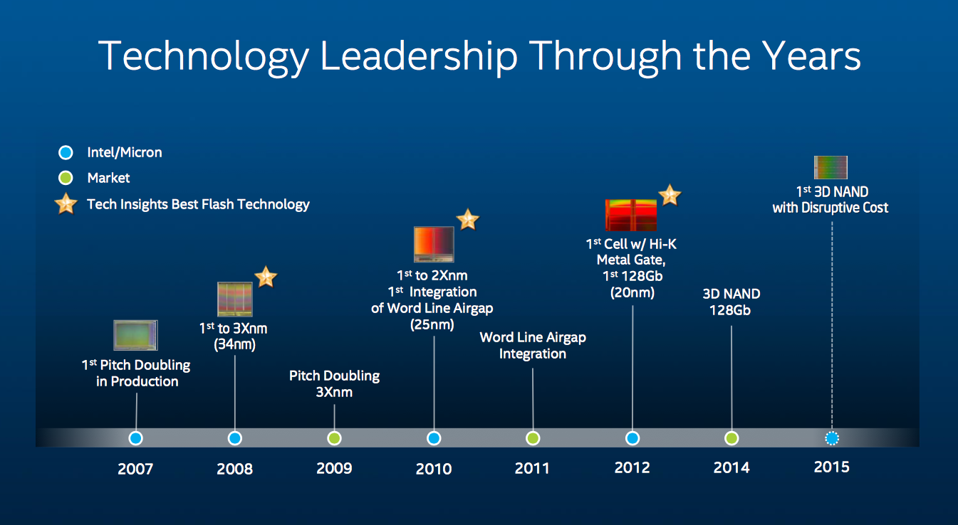
Following Samsung development of V- NAND Intel introduce their version of 3D NAND (see below). One of the benefits of 3D flash memories is the capability of using larger design rules such as 30-40 nm instead of scaling the design rules to smaller than 20nm.

One of the key problem of shrinking to smaller design rules than 20nm is the cost and complexity of multi-patterning photolithography and EUV lithography difficulties (ASML: Next-gen chipmaking tool ready forproduction in 2016 ). In addition, the reliability of the flash memory degrades when the memory cells become too close to each other.

"Samsung consciously went from a 24-layer 128Gbit MLC die to a 32-layer 86Gbit MLC die. In other words, Samsung could have upped the die capacity to ~170Gbit by just adding the extra layers, but the company chose to go with a smaller die instead. Smaller capacity dies have advantages in performance (higher parallelism) and applicability because eMMC/microSD devices have very strict die size constraints, "

Samsung only use 24 layers in fabricating the chips in order to increase the yield, which reduces the cost of working dies on each wafer. Adding layers that has to be manufactured with precise alignment and low defect density lengthen the learning curve of fabricating working dies. Intel is trying to catch up with Samsung which is already making the second generation of 3D NAND (Samsung 3D Process Pioneers Next Gen Semiconductor Devices ).


Ron
Insightful, timely, and accurate semiconductor consulting.
Semiconductor information and news at - http://www.maltiel-consulting.com/


Intel's 3D NAND to Ship in H2'15: 256Gbit Die

 & 32 Layers

by Kristian Vรคttรถ on November 25, 2014 5:20 AM EST
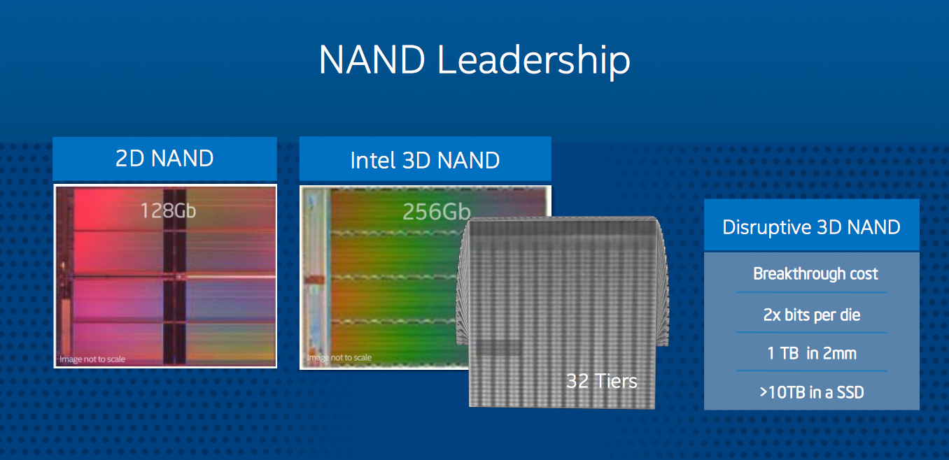
Last Thursday in its annual Investor Meeting Intel revealed the first details of its 3D NAND technology and announced that it will begin the shipments of 3D NAND in the second half of 2015. While Intel's investment in 3D NAND hasn't been a secret, the company has been relatively quiet about any specifics and the vital specs such as the number of layers and die capacity have remained unknown. In Thursday's webcast, Rob Crooke, Senior VP and General Manager of Intel's non-volatile memory group, disclosed that Intel's first generation 3D MLC NAND die will be 256Gbit (32GB) in capacity and will consist of 32 layers. The technology also enables a 384Gbit (48GB) TLC (3-bit-per-cell) die as we have learned over the years.
Intel claims that its 3D NAND is the most cost effective on the market and bases this on the fact that its die is 256Gbit whereas Samsung's is only up to 128Gbit at the moment. I'm not sure if I buy Intel's claim because while it's true that a higher capacity die results in higher array efficiency (i.e. peripheral circuitry takes less area), Samsung consciously went from a 24-layer 128Gbit MLC die to a 32-layer 86Gbit MLC die. In other words, Samsung could have upped the die capacity to ~170Gbit by just adding the extra layers, but the company chose to go with a smaller die instead. Smaller capacity dies have advantages in performance (higher parallelism) and applicability because eMMC/microSD devices have very strict die size constraints, so that might be a part of the reason why Samsung's strategy is so different from Intel's and Micron's. 
NAND Die Size
As the graph above shows, Intel's/Micron's NAND dies have historically been larger than the competitors', so the die capacity alone isn't enough to dictate whether Intel's 3D NAND is more cost efficient than Samsung, especially because both have 32 layers. Unlike Samsung, Intel didn't reveal the lithography that is used to manufacture the 3D NAND, but I would say it's safe to assume that the lithography is in the order of 30nm or 40nm because the whole idea of 3D NAND is to move away from multi-patterning to cut costs and with today's technology the smallest pitch of single-patterning is somewhere between 30nm and 40nm. Either way, it will be very interesting to see how Intel's 3D NAND stacks up against Samsung's because there are also some structural differences that affect the production cost as well as performance and endurance, but I'll save the structural analysis for a future article.
Intel said that 3D NAND technology will enable +10TB SSDs in the 'next couple of years', but it wasn't clear whether that is with first generation 3D NAND or some later generation with more layers and higher die capacity. Currently Intel's lineup tops out at 2TB (P3700 & P3600) with a 128Gbit die, so the 256Gbit die alone isn't enough to bring the capacities above 10TB. With effective controller development it should certainly be possible to build a 10TB SSD with a 256Gbit die, although I'm still inclined to believe that Mr. Crooke was referring to second or third generation 3D NAND with his statement. 
Similar to Intel's previous NAND efforts, 3D NAND has been jointly developed with Micron and will most likely be manufactured in the co-owned Utah plant as Intel sold its share in other fabs a couple of years ago. Interestingly enough, Mr. Crooke said that they also have the ability to bring 3D NAND production to an Intel fab, although to me that sounded more like a statement of technological possibility rather than a hint of future strategy. I wouldn't rule it out, though, but like Mr. Crooke said in the Q&A, Intel needs to have significant competitive advantage for it to make sense. In the past Intel's NAND technologies have generally been slightly ahead of the rest of the industry, but at least as of now Intel doesn't seem to have any substantial advantage in 3D NAND technology as Samsung is already shipping a 32-layer die and will likely ship a 48-layer die before Intel ships its 32-layer product.
All in all, we'll likely get more crumbs of information as the second half of 2015 gets closer. Given Intel's recent SSD strategy, I expect 3D NAND to first find its way to enterprise-class SSDs, but we'll see soon enough.

Wednesday, August 6, 2014

Top Semiconductor (1st Qtr 2014) Vendors

IC Insights have a new report about the top semiconductor ranking (see below).

"The ranking by IC Insights include three pure-play foundries (TSMC, GlobalFoundries, and UMC) and six fabless companies. It is interesting to note that the top four semiconductor suppliers all have different business models. Intel is essentially a pure-play IDM, Samsung a vertically integrated IC supplier, TSMC a pure-play foundry, and Qualcomm a fabless company, as observed by IC Insights."


As mentioned previously ( Top 25 2011 Semiconductor Sales Ranking) NAND market growth is not well document here. It is important to note that the semiconductor sales and growth rankings do not include SanDisk's $5.66B sales in 2011 and more than $6 Billion in 2013.


Ron
Insightful, timely, and accurate semiconductor consulting.
Semiconductor information and news at - 
http://www.maltiel-consulting.com/


Top 20 semiconductor vendors in 1Q2014


Date: 03/08/2014
The top-20 semiconductor ranking in Q1 2014 is quite a mix of companies with different product focus. The ranking by IC Insights include three pure-play foundries (TSMC, GlobalFoundries, and UMC) and six fabless companies. It is interesting to note that the top four semiconductor suppliers all have different business models. Intel is essentially a pure-play IDM, Samsung a vertically integrated IC supplier, TSMC a pure-play foundry, and Qualcomm a fabless company, as observed by IC Insights.

The further finding shared by IC Insights include:

IC foundries are included in the top 20 ranking because IC Insights has always viewed the ranking as a top supplier list, not as a market share ranking, and realizes that in some cases semiconductor sales are double counted. With many of our clients being vendors to the semiconductor industry (supplying equipment, chemicals, gases, etc.), excluding large IC manufacturers like the foundries would leave significant “holes” in the list of top semiconductor suppliers. Foundries and fabless companies are clearly identified in Figure 1. In the April Update to The McClean Report, market share rankings of IC suppliers by product type were presented and foundries were excluded from these listings.

It should be noted that not all foundry sales should be excluded when attempting to create marketshare data. For example, although Samsung had a large amount of foundry sales in the first quarter, most of its sales were to Apple. Apple does not re-sell these devices, so counting these foundry sales as Samsung semiconductor sales does not introduce double counting.

Overall, the list shown in Figure 1 is provided as a guideline to identify which companies are the leading semiconductor suppliers, whether they are IDMs, fabless companies, or foundries.


top semiconductor 20 2014

Figure 1

Outside of the top five spots, there were numerous changes within the 1Q14 top-20 semiconductor supplier ranking. As shown, MediaTek jumped up four positions in 1Q14 as compared to 1Q13 into 12th place. MediaTek continues to experience extremely strong demand for its devices in the booming low-end smartphone business in China and other Asia-Pacific locations. Moreover, MediaTek and MStar finalized their merger on February 1, 2014. Annual post-merger sales for MediaTek are expected to be well over $6 billion.

After Avago’s purchase of LSI Corp. on May 6, 2014, the combined annual semiconductor sales run-rate of the two companies is likely to be over $5 billion. Also, last year’s Micron/Elpida merger essentially created a new “giant” semiconductor company with Micron’s sales expected to be over $17 billion this year!

It should be noted that the sales of Micron and Elpida (merged on July 1, 2013), MediaTek and MStar, and Avago and LSI use the combined sales of the two companies for both 1Q13 and 1Q14, regardless of when the merger actually occurred. This was done in an attempt to make the company’s 1Q14/1Q13 sales growth rates more directly comparable and give a clearer picture of the merged company’s sizes going forward.

Another potential merger to keep a watch for in the future is Fujitsu and Panasonic. In February of this year, the two Japan-based companies signed a memorandum of understanding to combine the two companies’ system LSI businesses and form a new fabless semiconductor company. IC Insights estimates that the combined 1Q14 semiconductor sales of these two companies was about $1.25 billion (down from $1.44 billion in 1Q13), which would have ranked the “merged” company as the sixteenth largest semiconductor company in the first quarter of this year.

In total, the top 20 semiconductor companies’ sales increased by 9% in 1Q14 as compared to 1Q13, which was two points higher than IC Insights’ current 7% forecast for total worldwide semiconductor market growth this year. As shown, it took total semiconductor sales of just over $1.0 billion to make the 1Q14 top 20 ranking.

Figure 2 shows that there was a 58-percentage-point range of year-over-year growth rates among the 1Q14 worldwide top 20 semiconductor suppliers—from +48% for MediaTek/MStar to -10% for ST (it should be noted that excluding the legacy ST-Ericsson products, ST’s 1Q14/1Q13 sales increased 1%).

top semiconductor 20 2014

Figure 2

The success of the fabless and fab-lite business models and the continued strong growth of the memory market are evident when examining the top 20 semiconductor suppliers that logged double-digit growth in 1Q14. As shown, 10 of the top 11 1Q14 performers were either memory suppliers (SK Hynix, Micron, and Samsung) or fabless/fab-lite companies (MediaTek, AMD, Infineon, Freescale, Avago/LSI, NXP, and Nvidia). 

Monday, March 3, 2014

Flash NAND, NOR, eMMC Market Growth

NAND market continues to grow while NOR continue to shrink (see article below). 

The reason for NAND dominance were explained on my May 2007 article on Long Term Trends in the NOR and NAND Markets .


Highlights from review of the IHS report in the article below:
"NAND product known as embedded multimedia card (eMMC) enjoyed record shipments in 2013 of more than 1 billion units, up a hefty 49 percent from 687 million in 2012. NAND revenue rose 28 percent to US$25.8 billion.
In comparison, NOR shipments last year fell 10 percent to 606 million units, with revenue down 15 percent to approximately US$3.0 billion....
The evolution of eMMC, in particular, has been rapid, with nearly annual enhancements to performance. As an economical choice for greater flash-memory densities, eMMC has become viable in high-end markets like smartphones and tablets, in which high-density storage capacity is required along with low-power consumption and a small footprint.
Embedded NAND’s utility has also now carried over from smartphones in its early use, to tablets. Last year, eMMC was the standard memory configuration for a vast majority of tablets, the only exception being the Surface Pro from Microsoft, which employs a SATA-interface solid-state drive.
The billion-unit shipment level of eMMC last year is a milestone, Yang remarked, and the product shows the way forward for managed NAND solutions by its deft handling of error correction and enhanced reliability at the solution level."
Ron
Insightful, timely, and accurate semiconductor consulting.
Semiconductor information and news at - http://www.maltiel-consulting.com/


NAND eMMC hits a record year, while NOR Flash shrinks further

 
NAND eMMC hits a record year, while NOR Flash shrinks further
Source: IHS Technology, February 2014

The global memory market presented a vivid picture of contrast last year given the wildly divergent fortunes of its two main segments, with spritely NAND offset by the sobering continued downturn of beleaguered NOR flash, according to a new report from IHS Technology.
On the one hand, the NAND product known as embedded multimedia card (eMMC) enjoyed record shipments in 2013 of more than 1 billion units, up a hefty 49 percent from 687 million in 2012. NAND revenue rose 28 percent to US$25.8 billion.
In comparison, NOR shipments last year fell 10 percent to 606 million units, with revenue down 15 percent to approximately US$3.0 billion.
The overall flash market in 2013 was worth US$28.8 billion, up from US$23.7 billion a year earlier, as shown in the attached figure.
“The key driver to NAND lies in its proliferating use for mobile consumer electronics, exemplified by the memory’s increasingly widespread application in devices like smartphones, tablets and notebook PCs,” said Michael Yang, senior principal analyst for memory & storage at IHS.
“Meanwhile, NOR’s once-broad portfolio of applications in low-end mobile handsets and desktop PCs has mostly matured, and its next killer market has yet to manifest.”
These findings are contained in the report, “Mobile & Embedded Memory Tracker – Q4 2013,” from the Semiconductors & Components service of IHS.
NAND memory, in the form of either raw NAND or eMMC, is now the standard memory used for most smartphones. The only exception is Apple’s iPhone, which uses its own managed NAND memory product.
The evolution of eMMC, in particular, has been rapid, with nearly annual enhancements to performance. As an economical choice for greater flash-memory densities, eMMC has become viable in high-end markets like smartphones and tablets, in which high-density storage capacity is required along with low-power consumption and a small footprint.
Embedded NAND’s utility has also now carried over from smartphones in its early use, to tablets. Last year, eMMC was the standard memory configuration for a vast majority of tablets, the only exception being the Surface Pro from Microsoft, which employs a SATA-interface solid-state drive.
The billion-unit shipment level of eMMC last year is a milestone, Yang remarked, and the product shows the way forward for managed NAND solutions by its deft handling of error correction and enhanced reliability at the solution level.
The rise of eMMC has also bred a new cast of suppliers. While Samsung remains dominant, players like SK Hynix, SanDisk and Toshiba are fiercely competitive and poised to gain ground.
The eMMC space, however, could see challenges this year. With growth slowing in the smartphone and tablet markets, there could be a possible oversupply of the memory type, in the process also leading to a possible large drop in eMMC average selling prices.
The steady decline of the NOR flash market began in 2007 and hasn’t stopped since. At its peak, the NOR market exceeded US$9 billion a year and last hit US$8 billion back in 2006—a far cry from its current numbers.
The NOR picture is also complicated by the contrasting outlook for its two sub-segments.
Parallel NOR, long used in computers for boot-code execution or serving as a storage medium for entry-level cellphones, will see its run in wireless devices come to an end sometime next year.
Parallel NOR will continue to be used in high-level industrial, medical, networking and military applications, but its exit from wireless will be a blow.
Meanwhile, serial peripheral interface (SPI) NOR, rival to parallel NOR, will go on to wider use in both wireless and consumer devices.
SPI NOR’s relative simplicity in design and low manufacturing cost will prove appealing, and the memory will be especially attractive to manufacturers of low-cost cellphones that need to keep a lid on expenses.
The shift from parallel to SPI NOR has also impacted their respective suppliers. Micron Technology and Spansion, the foremost producers of parallel NOR, now also have SPI offerings.
However, both companies have been at pains to differentiate their SPI product from the rest of the pack, in order to stave off the aggressive penetration of other SPI NOR suppliers such as Macronix, Winbond Electronics and GigaDevice.
The ongoing growth of SPI NOR will help offset a shrinking parallel NOR market, but the industry would be healthier if consolidation took place and reduced the number of players to four, IHS believes.
There are five suppliers at present that command 75 percent of the market, along with a spattering of smaller producers that make up the rest of the market.
Even so, there are no quick fixes, with the largest NOR applications disappearing or on their way out, and new deployments like automotive NOR still facing an uphill climb.