Showing posts with label storage. Show all posts

Thursday, June 16, 2016

Cavium Buys QLogic (Storage, Networking Merger)

Another semiconductor merger

"Cavium Inc. will take on Broadcom, Intel and Mellanox in storage and networking with its billion-dollar acquisition of Qlogic Corp. The deal teams one of the semiconductor’s fastest growing companies with one just starting to emerge from a decline.

The acquisition adds Qlogic’s Fibre Channel and Ethernet controllers and boards to Cavium’s line up of communications, security and general-purpose processors, positioning Cavium as more of a full-line supplier to data centers. "

Other developments in networking chips-  Stanford Professor’s Startup Plans Novel Networking Chips.

Additional information on recent semiconductor mergers and acquisitions and China efforts- Update:China 2015/2016 Semiconductor Mergers, Acquisitions


Ron
Insightful, timely, and accurate semiconductor consulting.
Semiconductor information and news at - http://www.maltiel-consulting.com/


Cavium Buys QLogic for $1B

Deal expands vendor of data center chips
6/15/2016 07:15 PM EDT 

Thursday, May 12, 2016

3D Semiconductor Evolution

http://www.3dincites.com/2016/01/2015-retrospective-outlook-2016-3d-nand-flash-one-upmanship/
Semiconductor companies have been building 3D devices (which are  vertical circuits above the silicon die edge surface) for the last couple years. They have been going in the vertical direction due to the complexity of shrinking the devices (see 2012  Moore's Law Slowwwing ). Samsung has been making 3D V-NAND since 2013 (see Samsung’s 1Tb SSD: 3D Vertical NAND ). Samsung is now using its vertical layer manufacturing know-how to increase its market share in V-NAND and DRAM. More about Samsung's progress below.

Ron
Insightful, timely, and accurate semiconductor consulting.
Semiconductor information and news at - http://www.maltiel-consulting.com/


As tide turns against chip industry, Samsung forges ahead of rivals


By Se Young Lee
Apr. 26, 2016, 7:02 PM Thomson Reuters

SEOUL (Reuters) - Gloom may be settling over much of the world's semiconductor industry but Samsung Electronics Co Ltd is expected to cope better than most due to its strong technological edge, enabling it to boost market share for some key products and possibly even lift revenue.
A plunge in PC sales and slower growth for smartphones globally has hit the sector hard, prompting Intel Corp to say this month it would cut up to 12,000 jobs.
Qualcomm has said fiscal third-quarter chip shipments could fall as much as 22 percent, while SK Hynix Inc on Tuesday reported a 65 percent slide in quarterly operating income - its weakest result in three years.
Samsung, which reports its first-quarter earnings on Thursday, is also hurting. Chip profits - which accounted for just under half of its overall 2015 operating income - are widely expected to fall, with some analysts predicting a drop of more than 10 percent in January-March from a year earlier.
But if its rivals are getting pummeled, the South Korean tech giant is merely bruised and is in many ways benefiting as clients shift towards premium power-conserving DRAM chips for smartphones, as well as solid-state drives for data storage using 3D NAND chips.
"The technological gap between Samsung and its competitors in fields such as DRAM and NAND has been widening lately, which helps the company avoid the rate of profit decline seen at other firms," said Song Myung-sub, an analyst at HI Investment & Securities.
Even with a first-quarter drop of around 10 percent, Samsung's chip operating profit is expected to be nearly five times that of SK Hynix.
The world's No. 2 chipmaker also happens to run the world's biggest smartphone business, giving it a captive customer for its chips that none of its rivals have.
"This is a safehouse they can go to," said Avril Wu, an analyst at research firm Trendforce.
Healthy initial sales for Samsung's new flagship Galaxy S7 smartphones are expected to be the main driver of first-quarter operating profit, which the firm has said likely rose 10.4 percent from a year earlier to 6.6 trillion won ($5.8 billion).

DOMINANT POSITION
Of its key products, analysts are most upbeat about Samsung's NAND chip prospects. Samsung was the first to mass produce NAND flash chips using a technology called 3D NAND, helping it assume a dominant position in higher-margin products such as solid-state hard drives for computers and servers.
BNP Paribas expects the South Korean firm's NAND revenue to climb 16 percent and NAND operating profit to jump 69 percent this year. Shipments will also likely outpace the industry average, allowing Samsung to seize more market share, it said in a report.
The technology is already contributing to Samsung's profits, analysts say, adding that this is not the case for main NAND rivals Toshiba Corp, SK Hynix and Micron Technology Inc which are estimated to be as much as three years behind.
Investors and analysts also point to Samsung's superior production technology for DRAM chips, saying the firm is ahead of its closest rivals by at least a year. It can mass produce smaller chips than rivals, which boosts performance and conserves power as well as increasing the number that can be made from a single wafer.
Samsung commanded 58 percent of the mobile DRAM market as of the fourth quarter of 2015, according to TrendForce. Mobile DRAM revenue also accounted for more than half of Samsung's overall DRAM sales for October-March, TrendForce's data shows.

(Reporting by Se Young Lee; Editing by Edwina Gibbs)

Thursday, March 3, 2016

Semiconductor Startup Acquisition in 2016

Not only large semiconductor companies merge ( Update: China 2015/2016 Semiconductor Mergers, Acquisitions), startups are also acquired. Cisco acquisition of  Leaba semiconductor (see below) would help Cisco to lock up the network through their own chips. 

This purchase is similar to Apple snapping up semiconductor companies several years ago to strengthen future growth while See September 2013 blog - How Apple Leverages its R&D


Ron
Insightful, timely, and accurate semiconductor consulting.
Semiconductor information and news at - http://www.maltiel-consulting.com/


Cisco to acquire Leaba Semiconductor for $320 million as buying spree continues


By Ron Miller on March 2, 2016


Cisco continued its buying spree today as it announced its intention to acquire Israeli chip designer Leaba Semiconductor for $320 million.Cisco sees this acquisition as a way to bolster its hardware catalog with highly advanced chip technology.

“By combining Leaba’s semiconductor expertise with the Cisco engineering team, we will accelerate our plans for Cisco’s next generation product portfolio and bring new capabilities to the market faster,” Rob Salvagno, head of Cisco’s M&A and venture investing team wrote in a blog post announcing the purchase.

When the deal closes, the Leaba team will report to Core Hardware Group, led by Cisco senior vice president, Ravi Cherukuri, according to the blog post.

The company actually doesn’t even have a shipping product yet, R Ray Wang, founder at Constellation Research told TechCrunch. “They haven’t even finished their prototype. This is an acqui-hire for next generation semi-conductor [technology]. Think networking at the chip level,” he said.

This is not the first time the Leaba founding team has launched and sold a cutting edge chip production company, according to report in Globes, an Israeli business publication. The founding team, which consists of CEO Eyal Dagan and CTO Ofer Eini sold Dune Networks to Broadcom for $178 million in 2009.

Today’s news comes just the day after the company announced it was buying CliQr, a cloud hybrid services management platform for $260 million and just about a month after it bought Jasper Technologies for $1.4 billion.

Cisco is walking a fine transformational line here. On one hand, the purchase pattern suggests that the company is trying to pivot from its networking hardware roots to a business centered around services as the CliQr and Jasper Technologies would suggest.

Much like IBM, Cisco is looking to the future and trying to use its cash hoard to make strategic purchases to help speed up that transition.
At the same time, it’s not quite ready to give up completely on its hardware roots and purchasing a leading-edge semiconductor company suggests that it is still looking to a future where it can continue to lead in the networking hardware space.

Wednesday, November 12, 2014

Samsung 3D Process Pioneers Next Gen Semiconductor Devices

Samsung is leading the semiconductor industry with a two year leads in development of 3D NAND (see the article below).


The basic 3D process could be applied to other technologies beside flash such as DRAM memory or logic. It enable increasing the number of the transistors on each dies without the need to shrink the design rules below 20nm.

It is a key advantages since you do not need to develop the very difficult EUV photolitography.

More about 3D NAND in August 2013 blog - Samsung’s 1Tb SSD: 3D Vertical NAND

It make sense for Samsung to apply 3D Flash first to enterprise SSD, where the growth rate is +40%.

See also Applied Materials development work on advance patterning  - Applied Materials Develops Advanced Patterning Solution for Memory Devices


Ron
Insightful, timely, and accurate semiconductor consulting.
Semiconductor information and news at - http://www.maltiel-consulting.com/


samsung_hwaseong_2optimized.jpg

An aerial view of Samsung's Hwaseong plant.
10 NOVEMBER 2014
Samsung Electronics is working to strengthen its position in the SSD market by increasing the profitability of its semiconductor memory business.
According to industry sources on Nov. 9, Samsung established a strategy to choose 3-bit V-NAND-based SSD as a new growth engine of its semiconductor memory business.
Since the productivity of 3-bit V-NAND is twice as high as 10 nm class planar NAND flash, the V-NAND is superior in price competitiveness, data processing speed, durability, and power efficiency. Thus, if the 3-bit V-NAND is featured in SSDs, it will increase the performance and price competitiveness of SSDs.
After its success in having a system to mass produce 3-bit V-NAND at the company's semiconductor plant in Hwaseong City near Seoul early last month, the Korean chip maker started to prepare for mass production at its 3D V-NAND production facility in Xian, China.
Considering that it normally takes six months to expand a mass production system to other plants, the industry anticipates that 3-bit V-NAND will be mass produced starting in May or April of next year.
The semiconductor plant in Hwaseong City produces mainly planar NAND flash for mobile devices, and thus it manufactures less than 100,000 V-NAND 300 mm wafers per month.
In contrast, the 3D V-NAND production facility in Xian, which commenced full operations in May, manufactures 300,000 to 400,000 sheets each month. However, the facility is considered to have capacity to produce more than 700,000 sheets.
Samsung aims to strengthen its dominant position in the market by increasing its share in the SSD market through the use of 3-bit V-NAND in SSDs.
The Korean company revealed that it will feature 3-bit V-NAND in SSDs starting next year at a conference call, following its announcement of results for the third quarter at the end of October.
Samsung's decision can be interpreted to mean that it intends to widen the gap with its rival companies in the global market by featuring 3-bit V-NAND in SSDs used in a data center environment and SSDs for PCs.
Market research firm IHS Technology recently reported that the world's largest memory chip maker will record US$3.277 billion in sales from SSDs in 2014, a 60 percent year-on-year gain. Its market share is expected to increase from 26 percent to 29 percent this year, which will put the firm in the top spot, followed by Sandisk with a 19 percent share, Intel (18 percent), Toshiba (9 percent), and Micron Technology (8 percent).
Currently, Samsung is the only company in the world that produces 3D V-NAND flash memory chips. The gap with rival companies in technology is generally acknowledged to be more than two years.
- See more at: http://www.businesskorea.co.kr/article/7217/focusing-ssds-samsung-mass-produce-3-bit-3d-nand-flash-ssd#sthash.vOPJFbm8.dpuf

Tuesday, August 26, 2014

Die Size, NAND, DRAM 3D Roadmaps

Die sizes of various NAND chips shown below is a good indication of potential cost advantage. However, if the smaller die is made on a more expensive fab manufacturing process, its die would not be cheaper. Only when the fab new process advance enough along the learning curve would the smaller die be cheaper .


The project roadmap for the transition to 3D manufacturing is at NAND, DRAM 3D-Transition Roadmaps


Ron
Insightful, timely, and accurate semiconductor consulting.
Semiconductor information and news at - 
http://www.maltiel-consulting.com/


Measuring Toshiba's 15nm 128Gbit MLC NAND Die Size

by Kristian Vättö on August 22, 2014 12:42 PM EST
At Flash Memory Summit, Toshiba was showcasing their latest 15nm 128Gbit MLC NAND wafer that has been developed in partnership with SanDisk. I simply could not resist to calculate the die size as Toshiba/SanDisk has not published it and die size is always the basis of any semiconductor cost analysis. 
Die Size
To estimate the die size, I used the same method as with Samsung's second generation V-NAND. Basically I just calculated the amount of dies in both X and Y axes of the wafer as that gives as an approximation of the die size since we know that the diameter of the wafer is 300mm. 
Bit Density
The 15nm node from Toshiba/SanDisk is extremely competitive. Its bit density is essentially equivalent to Samsung's V-NAND, so it is no wonder that Toshiba and SanDisk are betting heavily on their 15nm node before moving to 3D in early 2016. Compared to other 2D NAND dies, the 15nm node is a clear winner from bit density standpoint as Micron's 16nm MLC does not even come close.
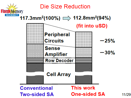
Toshiba's and SanDisk's secret lies in two-sided sense amp and all bit line (ABL) architecture, which reduce the size of the peripheral circuits and sense amplifier, resulting in higher memory array efficiency. Based on my estimation, the array efficiency (i.e. how big portion of the die is dedicated to memory cells) is about 80%, which is typical for a 128Gbit capacity. Higher capacities tend to yield better array efficiency since the peripheral circuitry does not scale as well as the memory cells do, so increasing the die capacity is one of the key solutions in lowering the cost per gigabyte.
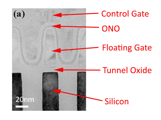
Since nobody has yet taken a cross-section of the 15nm die, it is hard to say for sure what Toshiba and SanDisk are doing to shrink the dimensions. There is no mention of high-K dielectrics, so that seems unlikely and if history is any guidance, then Toshiba/SanDisk is simply increasing the aspect ratio by making the floating gate taller to compensate for the smaller feature size and keep the overall floating gate volume similar. That also helps to maintain the gate coupling ratio because the control gate is still wrapped around the floating gate and with a taller floating gate the capacitance between the gates should remain sufficient despite the increasing proximity of the floating gates. 
The production of Toshiba/SanDisk 15nm NAND node is currently ramping up and SSDs based on the new node are expected in Q4'14.

Monday, June 16, 2014

SSD Market Share/ SanDisk buys Fusion-io

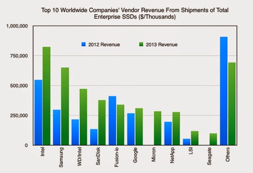
A recent survey by Gartner (see below) shows Intel and Samsung leading in shipment of SSD storage for enterprise.


Ron
Insightful, timely, and accurate semiconductor consulting.
Semiconductor information and news at - http://www.maltiel-consulting.com/


 IBM officially biggest all-flash array shipper - analyst

Gartner AFA data hits the street
By Chris Mellor13 Jun 2014 

No, it isn’t the greatly anticipated all-flash array magic quadrant, but it's great Gartner analysis nonetheless. The number-crunchers at Gartner HWQ have produced a Market Share Analysis: SSDs and Solid-State Arrays, Worldwide, 2013. Yummy. Let’s see what’s inside.
The doc, available as a download from Pure Storage (guess who's done well in the analysis) after registering a few details. It looks at both SSDs and all-flash arrays, which Gartner calls Solid State Arrays (SSAs) and IBM comes out as the leading SSA shipper – with Pure Storage second.
SSAs are defined carefully: ”SSAs are scalable, dedicated, solutions based solely on solid-state semiconductor technology for data storage that cannot be configured with HDD technology at any time. As distinct from SSD-only racks within ECB storage arrays, an SSA must be a stand-alone product denoted with a specific name and model number, which typically (but not always) includes an operating system and data management software optimised for solid-state technology.”
To cut a long story short, Dell and HDS all-flash array products are excluded, as are all-flash versions of – for example – EMC VMAX and VNX, and NetApp FAS arrays.
The SSD category embraces PCIe flash cards and also includes “self-contained solid-state NAND dual in-line memory modules (DIMMs), which must be used in dedicated slots in servers. Mainstream PC SSDs being used in servers are counted in this category due to end consumption.”
We’ll graph the information here, and you can read the detailed numbers by downloading the doc. The SSD info starts with worldwide vendor revenues:
Click chart for larger version
Total SSD revenues in 2012 were $7.2 billion, and in 2013 had risen to $10.99 billion, a 53.1 per cent increase.
Samsung as top dog got most of that with Intel, growing less, at number 2. Look at Sandisk’s rocketing growth up into the no 3 slot, closely followed by Micron. Toshiba held its fifth place but didn’t grow much. WD grew, Fusion-io declined and now we’re in the tail-enders.
Now let’s look at the enterprise SSD market:


Intel is top dog, not second-placed Samsung. WD, with its HGST/Intel SSDs is in third place followed by SanDisk successfully exhibiting its enterprise supplier credentials. Then there’s Fusion-io, which declined 2012 - 2013, Google with its internal use - amazing - Micron is a, we think, in a disappointing sixth place, NetApp a, for it, strong seventh then LSI and Seagate. EMC does not appear at all.
Now for the SSA numbers.
Here are the vendor revenue market share numbers:

Click chart to make it larger.
And here the actual SSA revenues by vendor:

Click chart to make it larger
IBM has had a wildly successful 2013 year, solidly overtaking Violin Memory to claim a dominating number 1 slot. Pure Storage has rocketed to the number 2 position in 2013 while Violin Memory slumped from first place in 2013 to third in 2013, illustrating the new management team’s uphill task. EMC has sprung into fourth place from a standing start and NetApp is not far behind in the fifth slot. Then there’s Nimbus Data and tail-ender Cisco - a dismal showing for the networking behemoth in our view, with startup SolidFire very close behind.
The SSA market was sized by Gartner at $236.5m in 2012, and 182.1 per cent higher at $667.3m in 2013. IBM’s SSA revenues grew at 278.1 per cent, Pure's at a magnificent 642.3 per cent and no other vendor outpaced the market, meaning they lost share.
Now this is artificial, as EMC, Kaminario, SolidFire and HP had no presence in Gartner’s numbers in 2013, but we can assert that Violin Memory, NetApp, Nimbus and Cisco all lost share from 2012 to 2013. With EMC, Kaminario, SolidFire and HP now in the SAA market we might expect these losses to continue in 2014.
The Gartner analysis contains more data, segment metrics and so forth. It’s worth a download and read if you’re interested.
Main takeaway? Big Blue really is big in SSAs, Pure Storage is living up to its hype, and the SSA market is growing at a fast lick. NAND the story goes on


Wednesday, May 14, 2014

3D NAND Race is On

[Image Source: Nikkei Electronics
Since Samsung announced their development of 3D NAND on August 2013 Samsung 3D Stacked NAND Flash has Engineering Samples . The other flash manufacturers have been trying to catch up while transitioning from planar NAND to 3D NAND. See below SunDisk and Toshiba announcement of their transitions plans (more information at 3D NAND Transition: 15nm Process Technology Takes Shape ).

Some background about 3D NAND and at 3D NAND flash is coming .  Also there is an interesting discussion regarding 3D flash from 2009 between Samsung and Toshiba 3D Cells Make Terabit NAND Flash Possible .


Ron
Insightful, timely, and accurate semiconductor consulting.
Semiconductor information and news at - http://www.maltiel-consulting.com/


 NAND Flash War

Toshiba, Sandisk Partnership to Mount Serious Challenge to Samsung

14 MAY 2014
Many computer memory chipmakers worldwide are said to be working to enlarge plants that produce NAND flash memory chips.  
According to the San Kei Shimbun on May 12, Toshiba, the world’s second-largest NAND flash memory chipmaker, decided to make an investment in a 3D V-NAND flash memory production facility in partnership with US-based semiconductor company SanDisk. Both companies are going to equally share the cost of the investment and inject 700 billion yen (7.419 trillion won, US$6.843 billion) for three years at the Yokkaichi Operation plant, the company’s memory production facility in Mie prefecture, Japan. At first, they estimated the amount at 400 billion yen. However, it nearly doubled after the two firms agreed to invest in the construction of a new facility and the replacement of the existing one.  
An increase in investment can be interpreted as Toshiba’s willingness to not lag behind its rival companies like Samsung Electronics, SK Hynix, and Micron. Given that Samsung completed the construction of its 3D V-NAND production facility in Xian, China on May 9, competition between Korean and Japanese firms to dominate the next-gen semiconductor memory market is expected to heat up again. 
Samsung began to mass-produce 3D V-NAND flash memory chips in its plant in Xian. 3D V-NAND flash memory where 40nm-class NAND flash memory is stacked up in 24 layers are twice as fast and last 10 times longer than 20nm-class planar NAND flash memory. The world’s largest computer memory chipmaker is planning to dominate the market by developing 3D V-NAND flash memory chips in a 36-layer stack soon.   
SK Hynix, the world's fourth-largest manufacturer of computer memory chips, is focusing on investing in NAND flash memory. For example, the firm converted its Cheongju M12 Plant that produced both DRAM and NAND flash memory chips into a NAND flash line last year in order to restructure the company whose focus was on DRAM. The chip-maker plans to mass-produce 3D V-NAND at the end of this year. Micron, which is in the third spot, recently changed its DRAM factory in Singapore into a NAND flash plant. 
Unlike its rivals, Toshiba only manufacturers NAND flash memory. Therefore, if competitors outperform the Japanese firm in the global NAND flash memory market, it will be fatal. Industry analysts are saying that Toshiba's lawsuit filed in March against SK Hynix for technology leakage despite its patent cross-licensing deal with the Korean firm was aimed at checking the Korean chip-maker's influence.  
According to the findings of market research firm IHS Technology, sales of NAND flash memory worldwide is estimated at US$25.8 billion last year, and the market continues to grow rapidly. In 2013, Samsung was the world's number one seller of computer memory chips with a 34.7 market share, followed by Toshiba (a 32.2 market share).

Friday, November 22, 2013

Facebook: Flash Storage in Database

Facebook continue to propel flash NAND memory usage in server and storage through open source implementations. See below more details on Flash Based Database.
“With the advent of flash storage, we are starting to see newer applications that can access data quickly by managing their own dataset on flash instead of accessing data over a network. These new applications are using what we call an embedded database.
“… When database requests are frequently served from memory or from very fast flash storage, network latency can slow the query response time. Accessing the network within a data center can take about 50 microseconds, as can fast-flash access latency. This means that accessing data over a network could potentially be twice as slow as an application accessing data locally. “
Additional technical details at Under the Hood: Building and open-sourcing RocksDB


More about Facebook Propels SSD Flash Storage


Ron
Insightful, timely, and accurate semiconductor consulting.
Semiconductor information and news at - http://www.maltiel-consulting.com/


Facebook’s latest open source effort: a flash-powereddatabase called RocksDB

by Derrick Harris


SUMMARY:

Facebook has open sourced a new embedded database called RocksDB that’s meant to take advantage of all the performance flash has to offer, from right on the application server. It might be a sign of best practices to come.

Facebook is on an open source roll lately, and on Thursday announced its latest open source project — an embedded key-value store called RocksDB. The company uses it to power certain user-facing applications that would suffer too much from having to access an external database over the network and to eliminate the certain problems relating to non-fully utilized IO performance on flash storage devices.

Facebook database engineer Dhruba Borthakur describes the design of and rationale behind RocksDB in some detail in a blog post, but the biggest factor leading to its creation might be the emergence of relatively inexpensive flash storage cards for servers (or, in Facebook’s case, custom-built servers packed entirely with flash).

“With the advent of flash storage, we are starting to see newer applications that can access data quickly by managing their own dataset on flash instead of accessing data over a network. These new applications are using what we call an embedded database.

“… When database requests are frequently served from memory or from very fast flash storage, network latency can slow the query response time. Accessing the network within a data center can take about 50 microseconds, as can fast-flash access latency. This means that accessing data over a network could potentially be twice as slow as an application accessing data locally. “

RocksDB was designed with these new hardware realities in mind, so it can take full advantage of the IOPS potential of flash memory as well as the computing power of many-core servers, Borthakur explains. Facebook has posted the results of a benchmark test running on a Fusion-io-powered server on the RocksDB GitHub page, and claims it’s significantly faster than Google’s LevelDB embedded key-value store.

From a broader IT perspective, RocksDB signals that the shifts in storage and computing economics that made the big data movement possible are now making their way into web application development, albeit using a storage media most organizations would consider using for storing “big data.” Facebook is performance hungry, but it’s also cost-sensitive, and it wouldn’t be storing “close to a petabyte of data across different applications,” as Borthakur writes, if the cost to do so was out of control.


He offered a handful of application types an embedded database like RocksDB is suitable for, including:

1. A user-facing application that stores the viewing history and state of users of a website.

2. A spam-detection application that needs fast access.

3. A graph-search query that needs to scan a data set in realtime.

4. RocksDB can be used to cache data from Hadoop, thereby allowing an app to query Hadoop data in realtime.

5. A message-queue that supports a high number of inserts and deletes.

In fact, Facebook has been finding all sorts of new ways to utilize flash as stepping stone between slow disks on one hand and expensive-but-fast RAM on the other.

Facebook is no doubt an early adopter of flash-heavy application architectures, but it’s also probably serving as a guiding light for other companies and their developers who want to achieve Facebook-like performance. As flash prices continue to drop — and now that Amazon Web Services is offering a whole suite of flash-backed instances on EC2 (the prices of which should also drop) — it’s conceivable we’re approaching an era of ever-better web and mobile applications that communicate with the network and the hard drive as little as possible.

Thursday, October 10, 2013

Facebook Propels SSD Flash Storage

Facebook continues to advance the frontier of flash NAND SSD in servers and data centers. The article bellow discusses  Flashcache and other open source projects.

"internally developed caching software, called Flashcache, to more efficiently use the thousands of solid-state drives (SSDs) that the social networking giant deploys to store frequently consulted data.
The newly released Flashcache 3.0 is able to make better decisions about what data to cache, while reducing the amount of wear and tear on expensive flash disks."
Earlier in the year Facebook asked for the cheapest and slowest flash memory
and Seven Questions for Facebook Infrastructure Guru Frank Frankovsky


Ron
Insightful, timely, and accurate semiconductor consulting.
Semiconductor information and news at -
http://www.maltiel-consulting.com/


Facebook open-source cache squeezes more from flash disks

Facebook continues to push the boundaries of storage and server technology in order to more quickly serve its billion users, and the results are being offered as open-source technology that can also benefit other companies.
Recently, Facebook updated its internally developed caching software, called Flashcache, to more efficiently use the thousands of solid-state drives (SSDs) that the social networking giant deploys to store frequently consulted data.
The newly released Flashcache 3.0 is able to make better decisions about what data to cache, while reducing the amount of wear and tear on expensive flash disks.
“With these improvements, Flashcache has become a building block in the Facebook stack,” wrote Domas Mituzas, a Facebook database engineer who authored a blog post explaining the updates to the open-source software.
The work aims to improve overall Facebook performance without unduly driving up operating costs.
“While the cost per GB for flash is coming down, it’s still not where it needs to be,” Mituzas wrote. Given the premium prices commanded for SSDs, Facebook doesn’t want to wear out these disks too quickly. “SSDs have limited write cycles, so we have to make sure that we’re not writing too much.”

Other open-source projects

Flashcache is one of a number of software projects that Facebook originally developed in house that the company has also released as open source. Earlier this year, for instance, the company also released a virtual machine, called HipHop, that speeds the processing of PHP code.
The company hopes that other organizations could reuse such programs as HipHop and Flashcache and eventually contribute to their further development. Like other open-source caching software such as memcache and Redis, Flashcache can be used to speed the responsiveness of a heavily visited website or popular Web application.
Facebook originally created Flashcache to boost the responsiveness of the MySQL databases that store user data. The software can be loaded onto the Linux kernel as a module without making any changes to the kernel itself.
The idea behind Flashcache is to use SSDs to hold the material that is most requested by users. SSDs tend to be faster than traditional rotating platter hard drives, though they are also more expensive by the GB when compared to hard drives. So it would not be cost-effective for Facebook to store all of its data on SSDs, especially if the vast majority of Facebook user data is rarely consulted.

FACEBOOK
Facebook found hotspots in its cache, where frequently consulted data could cluster in small areas, causing bottlenecks.
Although designed to work with MySQL and the MySQL InnoDB database storage engine, Flashcache can be used as a general caching mechanism for Linux systems.

Flashcache can also speed times it takes to write data to disk, from the user’s perspective, by saving newly updated data on SSD first and then writing it to the hard drives later.
The updated Flashcache module improves performance in read-write distribution, cache eviction and write efficiency.
Analyzing Flashcache performance, Facebook had found that most of its caches have a small subset of data that is read much more frequently than most of the other data.
With the previous version of Flashcache, 50 percent of a cache’s contents accounted for 80 percent of disk operations. Such a concentration of frequently consulted material could cause performance bottlenecks.
To improve Flashcache’s read-write distribution, the engineers developed a number of techniques to automatically position the data so that cache reads are distributed more evenly across the SSD. Now 50 percent of the cache accounts for 50 percent of the disk operations.
To improve the process of determining which data to move off the cache, a process called cache eviction, Flashcache switched from using the FIFO (first in first out) algorithm—in which the oldest data in the cache is removed first to make room for new data—to a LRU (least recently used) algorithm, which discards the data that hasn’t been requested for the longest period of time.
Improvements were also made in write efficiency.
Previously the software would write to disk only when it had a certain amount of data that was ready to be written. This resulted in uneven performance across different caches, however. So, Facebook engineers developed an approach that would write the cached data to disk whenever a copy of that data was requested by a user, which resulted in a smoother flow of write operations.
Thanks to these improvements, the updated caching mechanism has an average hit rate—or information that is requested by users that resides in cache—of 80 percent, up from 60 percent in the previous version. This means more data is served more quickly.
Updating the software has also slashed server I/O (input/output) required to read data by 40 percent, and reduced the I/O required to write data by 75 percent. For a company that is running thousands of servers, such a reduction in traffic can help make more efficient use of servers and keep hardware costs manageable.