Showing posts with label process expert. Show all posts

Monday, June 13, 2016

Semiconductor Fabrication Growth for 2016 and 2017

Estimates by SEMI.org for 2016 and 2017 fab growth are in the article below. 

However Intel/ Micron's XPoint memory introduction in 2016 and developments of other type of 3D processing will impact fab lines capacity and the growth of semiconductor processing equipment.

Some key points from the article:
"Fab equipment spending- ....activity in the 3D NAND, 10nm Logic, and Foundry segments is expected to push equipment spending up to $36 billion in 2016, 1.5% over 2015, and to $40.7 billion in 2017, up 13%."

"leading-edge technologies...also in 3D technologies....more conversions of older fabs may take place, but also additional new fabs and lines may begin construction."


3D process demand for etch and deposition is already impacting Applied Materials; see their recent quarterly results - Orders for the second quarter were $3.45 billion, up 37% from ayear earlier


Ron
Insightful, timely, and accurate semiconductor consulting.
Semiconductor information and news at - http://www.maltiel-consulting.com/


By David Manners  10th June 2016

Nineteen new fabs and lines are forecasted to begin construction in 2016 and 2017, according to SEMI.
While semiconductor fab equipment spending is off to a slow start in 2016, it is expected to gain momentum through the end of the year. For 2016, 1.5% growth over 2015 is expected while 13% growth is forecast in 2017.
Fab equipment spending – including new, secondary, and in-house – was down 2% in 2015. However, activity in the 3D NAND, 10nm Logic, and Foundry segments is expected to push equipment spending up to $36 billion in 2016, 1.5% over 2015, and to $40.7 billion in 2017, up 13%.
Equipment will be purchased for existing fabs, lines that are being converted to leading-edge technology, as well as equipment going into new fabs and lines that began construction in the prior year.
Table 1 shows the regions where new fabs and lines are expected to be built in 2016 and 2017. These projects have a probability of 60% or higher, according to SEMI’s data. While some projects are already underway, others may be subject to delays or pushed into the following year.
Breaking down the 19 projects by wafer size, 12 of the fabs and lines are for 300mm (12-inch), four for 200mm, and three LED fabs (150mm, 100mm, and 50mm). Not including LEDs, the potential installed capacity of all these fabs and lines is estimated at almost 210,000 wafer starts per month (in 300mm equivalents) for fabs beginning construction in 2016 and 330,000 wafer starts per month (in 300mm equivalents) for fabs beginning construction in 2017.
In addition, the transition to leading-edge technologies (as we can see in planar technologies, but also in 3D technologies) creates a reduction in installed capacity within an existing fab. To compensate for this reduction, more conversions of older fabs may take place, but also additional new fabs and lines may begin construction.


Thursday, May 12, 2016

3D Semiconductor Evolution

http://www.3dincites.com/2016/01/2015-retrospective-outlook-2016-3d-nand-flash-one-upmanship/
Semiconductor companies have been building 3D devices (which are  vertical circuits above the silicon die edge surface) for the last couple years. They have been going in the vertical direction due to the complexity of shrinking the devices (see 2012  Moore's Law Slowwwing ). Samsung has been making 3D V-NAND since 2013 (see Samsung’s 1Tb SSD: 3D Vertical NAND ). Samsung is now using its vertical layer manufacturing know-how to increase its market share in V-NAND and DRAM. More about Samsung's progress below.

Ron
Insightful, timely, and accurate semiconductor consulting.
Semiconductor information and news at - http://www.maltiel-consulting.com/


As tide turns against chip industry, Samsung forges ahead of rivals


By Se Young Lee
Apr. 26, 2016, 7:02 PM Thomson Reuters

SEOUL (Reuters) - Gloom may be settling over much of the world's semiconductor industry but Samsung Electronics Co Ltd is expected to cope better than most due to its strong technological edge, enabling it to boost market share for some key products and possibly even lift revenue.
A plunge in PC sales and slower growth for smartphones globally has hit the sector hard, prompting Intel Corp to say this month it would cut up to 12,000 jobs.
Qualcomm has said fiscal third-quarter chip shipments could fall as much as 22 percent, while SK Hynix Inc on Tuesday reported a 65 percent slide in quarterly operating income - its weakest result in three years.
Samsung, which reports its first-quarter earnings on Thursday, is also hurting. Chip profits - which accounted for just under half of its overall 2015 operating income - are widely expected to fall, with some analysts predicting a drop of more than 10 percent in January-March from a year earlier.
But if its rivals are getting pummeled, the South Korean tech giant is merely bruised and is in many ways benefiting as clients shift towards premium power-conserving DRAM chips for smartphones, as well as solid-state drives for data storage using 3D NAND chips.
"The technological gap between Samsung and its competitors in fields such as DRAM and NAND has been widening lately, which helps the company avoid the rate of profit decline seen at other firms," said Song Myung-sub, an analyst at HI Investment & Securities.
Even with a first-quarter drop of around 10 percent, Samsung's chip operating profit is expected to be nearly five times that of SK Hynix.
The world's No. 2 chipmaker also happens to run the world's biggest smartphone business, giving it a captive customer for its chips that none of its rivals have.
"This is a safehouse they can go to," said Avril Wu, an analyst at research firm Trendforce.
Healthy initial sales for Samsung's new flagship Galaxy S7 smartphones are expected to be the main driver of first-quarter operating profit, which the firm has said likely rose 10.4 percent from a year earlier to 6.6 trillion won ($5.8 billion).

DOMINANT POSITION
Of its key products, analysts are most upbeat about Samsung's NAND chip prospects. Samsung was the first to mass produce NAND flash chips using a technology called 3D NAND, helping it assume a dominant position in higher-margin products such as solid-state hard drives for computers and servers.
BNP Paribas expects the South Korean firm's NAND revenue to climb 16 percent and NAND operating profit to jump 69 percent this year. Shipments will also likely outpace the industry average, allowing Samsung to seize more market share, it said in a report.
The technology is already contributing to Samsung's profits, analysts say, adding that this is not the case for main NAND rivals Toshiba Corp, SK Hynix and Micron Technology Inc which are estimated to be as much as three years behind.
Investors and analysts also point to Samsung's superior production technology for DRAM chips, saying the firm is ahead of its closest rivals by at least a year. It can mass produce smaller chips than rivals, which boosts performance and conserves power as well as increasing the number that can be made from a single wafer.
Samsung commanded 58 percent of the mobile DRAM market as of the fourth quarter of 2015, according to TrendForce. Mobile DRAM revenue also accounted for more than half of Samsung's overall DRAM sales for October-March, TrendForce's data shows.

(Reporting by Se Young Lee; Editing by Edwina Gibbs)

Tuesday, September 29, 2015

Surprise, Samsung's A9 Processor is 9% Smaller than TSMC''s in iPhone 6s


Chipworks reversed engineered Samsung's and TSMC's A9
Apple is using both Samsung and TSMC to fabricate the microprocessor for the new iPhone 6 and 6s (see the article below). A second source is typically used to cut down the risk of depending on only one fab for key component.  It is very interesting that the die size of Samsung is 96 mm2 while TSMC die size is 8.85% larger at 104.5 mm2.

Apple improved the approach of using a second source. It implemented two versions at the same time. When you develop new complex products such as A9 with an embedding mobile processor inside A9 , there are risks that the new processor would not work. By using one design at TSMC, and a shrunk version at Samsung, Apple got ahead on the learning curve. It gave Apple a chance to implement improvement while shrinking the die. In addition, the shrunk die at Samsung reduces the cost of the A9 die.

It will be interesting to know if there are some performance differences between Samsung and TSMC versions.


Ron
Insightful, timely, and accurate semiconductor consulting.
Semiconductor information and news at - http://www.maltiel-consulting.com/


Chipworks: Both Samsung and TSMC are making the A9 chip for Apple

And the Samsung version is smaller than the TSMC version.


The only thing that most people will need to know about Apple's A9 is that it's a whole lot faster than last year's A8. But for those of you who are more interested in chip design, Chipworks has unearthed an interesting tidbit: there are two different versions of the A9 chip, one manufactured by Samsung and another by Taiwan Semiconductor (TSMC). Most interestingly, Samsung's version (the APL0898) has a slightly smaller footprint than the TSMC version (APL1022).
There have long been rumors that Apple was dual-sourcing the A8 from Samsung and TSMC, but this is the first visual proof that we've seen of the practice. iPhone and iPad processors up to and including the A7 were all made by Samsung.
Apple buys other parts from multiple sources including NAND flash and RAM, but the SoC is a major component with bigger implications for performance and power. Chipworks promises a more in-depth look at how the two processors are different, but for now, all we know is that they differ in size.
We have no way to confirm whether the chips in our review samples were made by Samsung or TSMC. iFixit's teardowns found the Samsung version of the A9 in the iPhone 6S and TSMC's version in the iPhone 6S Plus, which makes sense—a larger phone has more room to spare for a larger chip—but that doesn't necessarily mean that all of the phones are being put together this way. In our testing, both the iPhone 6S and 6S Plus benchmarked nearly identically, and both behaved well during Geekbench's thermal throttling test.

Monday, December 15, 2014

Samsung's 3D NAND Teardown, Patent

Andrew Walker at 3dincites.com analyzes Samsung 3D V-NAND below.

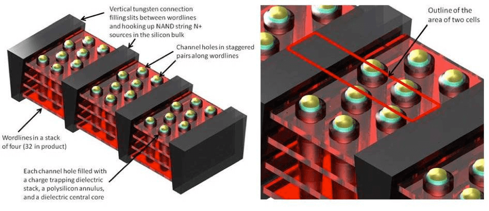
Andrew Walker's  vertical channel 3D NAND based on Chipworks’ cross section of Samsung’s 86 Gbit 32-layer 2nd generation V-NAND


The article below calculate cell size based on Techinsights teardown and wonders about benefits of this technology. However, there are key benefits for Samsung due to the difference in yield and cost of increasing the number of CVD layers vs reducing photolithography layers and masks cost and the associate increase in yield.

More from November 2012 -  3D NAND flash is coming


A 2009 patent application by Samsung for this technology is - US20100155810


Ron
Insightful, timely, and accurate semiconductor consulting.
Semiconductor information and news at - http://www.maltiel-consulting.com/


Samsung’s 3D V-NAND Flash Product: Ceaselessly Marching

What a feast of information Techinsights has given us on Samsung’s 32-layer 3D V-NAND product! By adding dimensions to the cross sections and including the orthogonal direction, we can now add to what we discerned last time and see how Samsung has built this engineering wonder. As a reminder, Figure 1 shows what I thought was a reasonable guess based on Chipworks analysis.
Figure 1: Generic vertical channel 3D NAND based on Chipworks’ cross section of Samsung’s 86 Gbit 32-layer 2nd generation V-NAND.
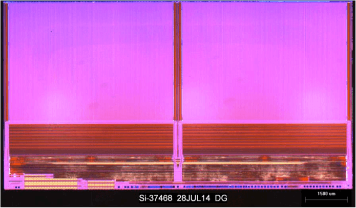
Notice that I couldn’t add real dimensions at the time. Now we can. But let’s first look at what Techinsights has provided. Figure 2 shows the die with a measurement bar allowing us to come out with the following: die size = 87.4 mm²; array efficiency = 66%.
FIGURE 2 – Die photo of Samsung’s 86 Gbit 32-layer 2nd generation V-NAND (courtesy Techinsights).
Figure 2: Die photo of Samsung’s 86 Gbit 32-layer 2nd generation V-NAND (courtesy Techinsights).
Figure 3 shows how the wordlines are connected in a staircase fashion. A space of about 20µm is needed.
Figure 3: How Samsung connects to the wordlines in the array (courtesy Techinsights).
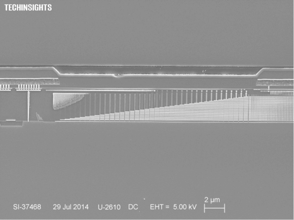
Figure 4 shows a SEM cross section made at the top of the array stack. This is similar to the one from Chipworks but now with the all-important measurement bar. With this, the long edge of the outline rectangle for two cells given in Figure 1 above is about 725nm. Also, the channel hole pitch in the same direction between the vertical tungsten slits is about 240nm. Don’t worry about remembering these numbers – we’ll summarize at the end in a figure.
Figure 4: Cross section of Samsung’s 86 Gbit 32-layer 2nd generation V-NAND at the top of the stack (courtesy Techinsights).
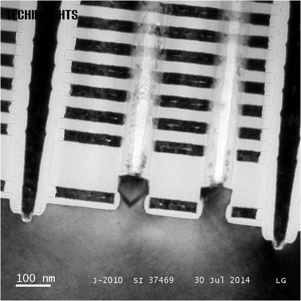
Figure 5 shows a beautiful cross section TEM image taken at the bottom of the stack and shows how the whole 3D memory array connects up to the wafer substrate.There are some interesting points to be highlighted from this, namely:
  1. The gate all-around access device at the bottom of the stack has a crystalline channel that looks like it has been epitaxially grown from the substrate. If you look carefully, you can make out where the epitaxial growth started which would have been the bottom of the channel hole etched into the wafer substrate.
  2. The polysilicon channel material rests on this pedestal of epitaxial silicon at the bottom of the hole.
  3. The vertical tungsten slits reach through to the silicon substrate which is probably where the NAND N+ doped sources are.
  4. The vertical tungsten slits are laterally isolated from the gate all-around tungsten wordlines.
  5. Vertical tungsten slit-to-slit space (the long edge of the outline rectangle for two cells given in Figure 1) is 730nm.
  6. Hole-to-hole pitch lying between the vertical tungsten slits is 245nm.
Figure 5; Cross-section TEM of Samsung’s 86 Gbit 32-layer 2nd generation V-NAND at the bottom of the stack (courtesy Techinsights).
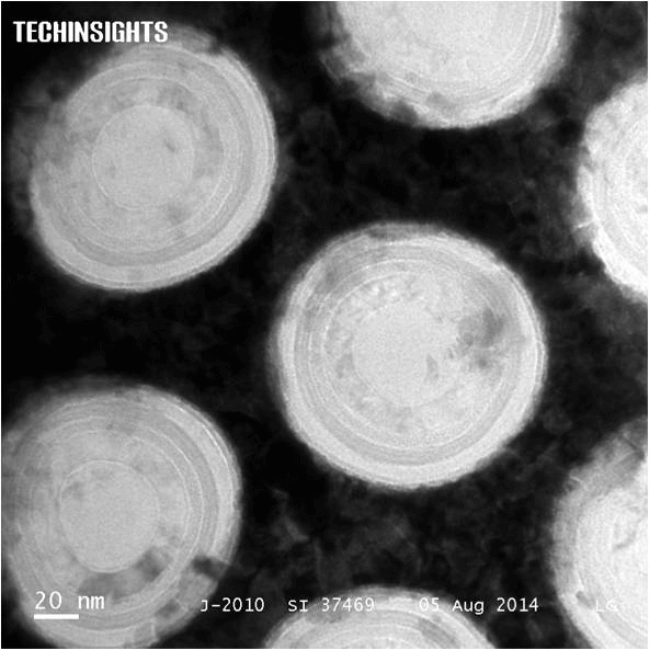
Figure 6 shows another beautiful TEM image of the channel holes taken staring down the holes. This one surely wins the prize! It looks like the picture’s y-axis aligns with the direction of the wordlines and the x-axis with the bitlines. In other words, the y-axis is orthogonal to the plane of Figures 4 and 5 above.
Figure 6: – TEM of Samsung’s 86 Gbit 32-layer 2nd generation V-NAND looking down the channel holes (courtesy Techinsights).
Figure 6 allows us to derive the following information:
  1. Hole-to-hole pitch to make it equivalent to the sectioned holes in the plane of Figures 4 and 5 (bottom left channel hole to bottom right channel hole in Figure 6) = 260 nm.
  2. Hole-to hole-pitch in the orthogonal direction (distance between a horizontal line in Figure 6 through a hole and another horizontal line through the hole that is placed offset to the first hole) = 80 nm.
  3. Diameter of channel hole (before ONO, polysilicon and dielectric core have been deposited) = 120nm.
  4. ONO thickness = 22 nm.
  5. Channel polysilicon thickness = 11 nm.
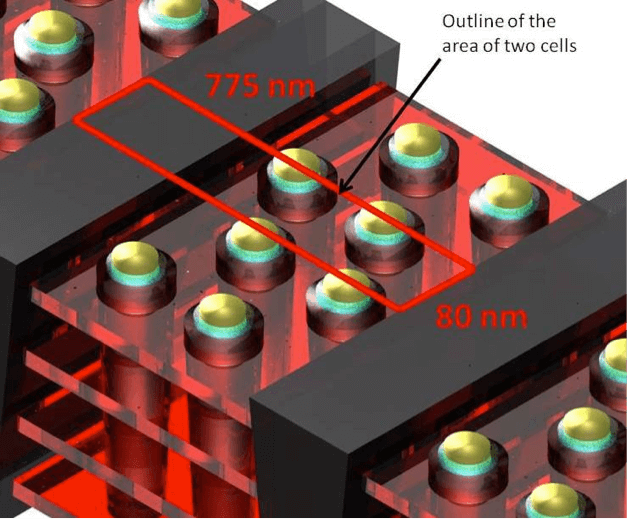
By taking the critical dimensions from the highest resolution TEM photo (Figure 6) since this will probably be more accurate than the other photos, we can redraw Figure 1 with the dimensions needed to calculate cell size. Note that the vertical tungsten slit to slit dimension has been scaled up slightly from that found in Figure 5 based on the hole to hole dimension calculated in Figure 6.
The final result shown in Figure 7 has two cells in a box of 775nm x 80nm. Therefore, the physical cell size on each layer is around 31000 nm². This is certainly more aggressive than what I had calculated previously but is still around 20F2 where F is 40 nm and remains around 24 times the area of Micron’s 16nm 2D cell.
Figure 7: – Final dimensional result for a box containing two physical cells in each layer. The effective physical cell size is 31000 nm².

Wednesday, November 12, 2014

Samsung 3D Process Pioneers Next Gen Semiconductor Devices

Samsung is leading the semiconductor industry with a two year leads in development of 3D NAND (see the article below).


The basic 3D process could be applied to other technologies beside flash such as DRAM memory or logic. It enable increasing the number of the transistors on each dies without the need to shrink the design rules below 20nm.

It is a key advantages since you do not need to develop the very difficult EUV photolitography.

More about 3D NAND in August 2013 blog - Samsung’s 1Tb SSD: 3D Vertical NAND

It make sense for Samsung to apply 3D Flash first to enterprise SSD, where the growth rate is +40%.

See also Applied Materials development work on advance patterning  - Applied Materials Develops Advanced Patterning Solution for Memory Devices


Ron
Insightful, timely, and accurate semiconductor consulting.
Semiconductor information and news at - http://www.maltiel-consulting.com/


samsung_hwaseong_2optimized.jpg

An aerial view of Samsung's Hwaseong plant.
10 NOVEMBER 2014
Samsung Electronics is working to strengthen its position in the SSD market by increasing the profitability of its semiconductor memory business.
According to industry sources on Nov. 9, Samsung established a strategy to choose 3-bit V-NAND-based SSD as a new growth engine of its semiconductor memory business.
Since the productivity of 3-bit V-NAND is twice as high as 10 nm class planar NAND flash, the V-NAND is superior in price competitiveness, data processing speed, durability, and power efficiency. Thus, if the 3-bit V-NAND is featured in SSDs, it will increase the performance and price competitiveness of SSDs.
After its success in having a system to mass produce 3-bit V-NAND at the company's semiconductor plant in Hwaseong City near Seoul early last month, the Korean chip maker started to prepare for mass production at its 3D V-NAND production facility in Xian, China.
Considering that it normally takes six months to expand a mass production system to other plants, the industry anticipates that 3-bit V-NAND will be mass produced starting in May or April of next year.
The semiconductor plant in Hwaseong City produces mainly planar NAND flash for mobile devices, and thus it manufactures less than 100,000 V-NAND 300 mm wafers per month.
In contrast, the 3D V-NAND production facility in Xian, which commenced full operations in May, manufactures 300,000 to 400,000 sheets each month. However, the facility is considered to have capacity to produce more than 700,000 sheets.
Samsung aims to strengthen its dominant position in the market by increasing its share in the SSD market through the use of 3-bit V-NAND in SSDs.
The Korean company revealed that it will feature 3-bit V-NAND in SSDs starting next year at a conference call, following its announcement of results for the third quarter at the end of October.
Samsung's decision can be interpreted to mean that it intends to widen the gap with its rival companies in the global market by featuring 3-bit V-NAND in SSDs used in a data center environment and SSDs for PCs.
Market research firm IHS Technology recently reported that the world's largest memory chip maker will record US$3.277 billion in sales from SSDs in 2014, a 60 percent year-on-year gain. Its market share is expected to increase from 26 percent to 29 percent this year, which will put the firm in the top spot, followed by Sandisk with a 19 percent share, Intel (18 percent), Toshiba (9 percent), and Micron Technology (8 percent).
Currently, Samsung is the only company in the world that produces 3D V-NAND flash memory chips. The gap with rival companies in technology is generally acknowledged to be more than two years.
- See more at: http://www.businesskorea.co.kr/article/7217/focusing-ssds-samsung-mass-produce-3-bit-3d-nand-flash-ssd#sthash.vOPJFbm8.dpuf

Wednesday, October 22, 2014

14nm FinFETs Technolgy

In the upcoming IEDM Intel will talk more about their 3D transistors using FinFET for the 14nm generation (see below). 


"Intel will reveal its processing secrets including its doping technique to prevent current leakage under the fins and to maintain very low doped fins, resulting in mitigation of variation, its use of two levels of air-gap-insulated interconnects at 80-and-160nm minimum pitches, yielding a 17% reduction in capacitance delays; eight layers of 52nm pitch interconnects embedded in low-k dielectrics"

Also IBM will discuss at IEDM adding SOI to FinFETs, which reduce their capacitance. SOI has been used by IBM for other processes, however it complicate designing circuits on the chips.


See more about FinFETs from May 2011 at - Tutorial: Intel 22nm 3D Tri-Gate FinFETs Transistors  

Ron
Insightful, timely, and accurate semiconductor consulting.
Semiconductor information and news at - http://www.maltiel-consultin


Intel, IBM Dueling 14nm FinFETS

IEDM reveals diametrically opposed approaches
10/21/2014 06:26 PM EDT 

Thursday, November 21, 2013

Hynix DRAM (Wuxi) Production


Hynix DRAM production was mentioned in an announcement of introduction of the 64Gb (gigabit) multi-level cell (MLC) NAND FLASH using the 16-nanometer micro fabrication process technology.
“The equipment, not directly damaged by the fire, requires a lot of work before it can be used again in the production line,” said an industry official. “It will not be as easy to normalize the Wuxi plant as originally thought.”

Fab equipment has to be meticulously cleaned before it can be put back in production. You have to make sure running the equipment would not produce particles. In addition every piece of equipment impacted by the fire need to be recalibrated.

Hynix also mentioned:
"SK Hynix raised the production capacity of the Icheon DRAM plant by 30% after the fire in the Wuxi plant in China. Early next year the company is considering making additional investments to extend the Icheon plant."

I am not clear how they can raise production 30% very quickly. They can shrink product masks set, improve production process, or buy new equipment. Each one will take several months to implement.


Ron

Insightful, timely, and accurate semiconductor consulting.
Semiconductor information and news at - http://www.maltiel-consulting.com/


SK Hynix concentrates investment in the microfabrication process…in a bid to chase ‘two hares’ at a time

2013/11/21 By Lee Hyeong-soo

SK Hynix (CEO Park Seong-wook) announced on November 20 that it began to produce the 64Gb (gigabit) multi-level cell (MLC) NAND FLASH using the 16-nanometer microfabrication process technology. 

It also completed the development of the 128Gb (16GB) package. It is the largest single 16-nanometer 64Gb MLC NAND FLASH chip. SK Hynix is planning to begin mass production of this product early next year. 
In general, as the microfabrication process intensifies, the interference between memory cells takes place. SK Hynix overcame the inter-cell interference during the 16-nanometer microfabrication process by applying the air gap technology, which fills the space between circuits with air, not an insulating material. 

SK Hynix is planning to convert the DRAM microfabrication process from upper 20-nanometer to lower 20-nanometer. Its strategy is to increase the global market share while raising the DRAM production capacity at the same time through the microfabrication process conversion. It is also reinforcing its product portfolio by concentrating on development of the triple-level cell (TLC) and 3D NAND FLASH. 

“We became the first in the world to commercialize the 16-nanometer microfabrication process technology, and completed the development of the 128Gb MLC product,” said Kim Jin-woong, head of the SK Hynix Flash Tech Innovation Division. “We can secure powerful competiveness in the NAND FLASH market.” 

SK Hynix seems to be concentrating on microfabrication process conversion because it intends to keep growing stably rather than impractical technology conversion. The top management, including CEO Park Seong-wook, is confident that it will not be behind Samsung Electronics as far as the microfabrication process technology is concerned. 

The recent fire in the Wuxi plant in China greatly influenced next year’s business strategy. SK Hynix believes that it is unreasonable to seek rapid changes, such as production of 3D semiconductors, when one of its global production bases, i.e. the Wuxi plant, is unstable. 

SK Hynix raised the production capacity of the Icheon DRAM plant by 30% after the fire in the Wuxi plant in China. Early next year the company is considering making additional investments to extend the Icheon plant. The Wuxi plant was expected to be normalized sometime this month, but there is a possibility of delay. 

SK Hynix is focused on recovering the production capacity while concentrating on investing in the Icheon DRAM line for the time being. If the microfabrication process conversion is successful, it will be able to achieve 7~8%ish growth next year without any additional investment in equipment. As the DRAM price skyrocketed, the fire of the Wuxi plant did not cause much financial damage, but if it does not defend the market share to a certain extent, it may boomerang in the future. DRAM also looks attractive in terms of profits. As the short supply continues, the DRAM price is continuously rising. 

“The equipment, not directly damaged by the fire, requires a lot of work before it can be used again in the production line,” said an industry official. “It will not be as easy to normalize the Wuxi plant as originally thought.” 

Lee Hyeong-soo | goldlion2@etnews.com