Showing posts with label 15nm. Show all posts

Tuesday, August 26, 2014

Die Size, NAND, DRAM 3D Roadmaps

Die sizes of various NAND chips shown below is a good indication of potential cost advantage. However, if the smaller die is made on a more expensive fab manufacturing process, its die would not be cheaper. Only when the fab new process advance enough along the learning curve would the smaller die be cheaper .


The project roadmap for the transition to 3D manufacturing is at NAND, DRAM 3D-Transition Roadmaps


Ron
Insightful, timely, and accurate semiconductor consulting.
Semiconductor information and news at - 
http://www.maltiel-consulting.com/


Measuring Toshiba's 15nm 128Gbit MLC NAND Die Size

by Kristian Vättö on August 22, 2014 12:42 PM EST
At Flash Memory Summit, Toshiba was showcasing their latest 15nm 128Gbit MLC NAND wafer that has been developed in partnership with SanDisk. I simply could not resist to calculate the die size as Toshiba/SanDisk has not published it and die size is always the basis of any semiconductor cost analysis. 
Die Size
To estimate the die size, I used the same method as with Samsung's second generation V-NAND. Basically I just calculated the amount of dies in both X and Y axes of the wafer as that gives as an approximation of the die size since we know that the diameter of the wafer is 300mm. 
Bit Density
The 15nm node from Toshiba/SanDisk is extremely competitive. Its bit density is essentially equivalent to Samsung's V-NAND, so it is no wonder that Toshiba and SanDisk are betting heavily on their 15nm node before moving to 3D in early 2016. Compared to other 2D NAND dies, the 15nm node is a clear winner from bit density standpoint as Micron's 16nm MLC does not even come close.
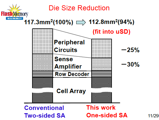
Toshiba's and SanDisk's secret lies in two-sided sense amp and all bit line (ABL) architecture, which reduce the size of the peripheral circuits and sense amplifier, resulting in higher memory array efficiency. Based on my estimation, the array efficiency (i.e. how big portion of the die is dedicated to memory cells) is about 80%, which is typical for a 128Gbit capacity. Higher capacities tend to yield better array efficiency since the peripheral circuitry does not scale as well as the memory cells do, so increasing the die capacity is one of the key solutions in lowering the cost per gigabyte.
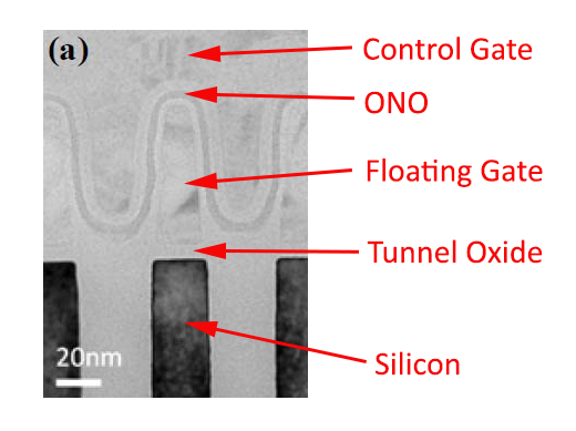
Since nobody has yet taken a cross-section of the 15nm die, it is hard to say for sure what Toshiba and SanDisk are doing to shrink the dimensions. There is no mention of high-K dielectrics, so that seems unlikely and if history is any guidance, then Toshiba/SanDisk is simply increasing the aspect ratio by making the floating gate taller to compensate for the smaller feature size and keep the overall floating gate volume similar. That also helps to maintain the gate coupling ratio because the control gate is still wrapped around the floating gate and with a taller floating gate the capacitance between the gates should remain sufficient despite the increasing proximity of the floating gates. 
The production of Toshiba/SanDisk 15nm NAND node is currently ramping up and SSDs based on the new node are expected in Q4'14.

Wednesday, May 14, 2014

3D NAND Race is On

[Image Source: Nikkei Electronics
Since Samsung announced their development of 3D NAND on August 2013 Samsung 3D Stacked NAND Flash has Engineering Samples . The other flash manufacturers have been trying to catch up while transitioning from planar NAND to 3D NAND. See below SunDisk and Toshiba announcement of their transitions plans (more information at 3D NAND Transition: 15nm Process Technology Takes Shape ).

Some background about 3D NAND and at 3D NAND flash is coming .  Also there is an interesting discussion regarding 3D flash from 2009 between Samsung and Toshiba 3D Cells Make Terabit NAND Flash Possible .


Ron
Insightful, timely, and accurate semiconductor consulting.
Semiconductor information and news at - http://www.maltiel-consulting.com/


 NAND Flash War

Toshiba, Sandisk Partnership to Mount Serious Challenge to Samsung

14 MAY 2014
Many computer memory chipmakers worldwide are said to be working to enlarge plants that produce NAND flash memory chips.  
According to the San Kei Shimbun on May 12, Toshiba, the world’s second-largest NAND flash memory chipmaker, decided to make an investment in a 3D V-NAND flash memory production facility in partnership with US-based semiconductor company SanDisk. Both companies are going to equally share the cost of the investment and inject 700 billion yen (7.419 trillion won, US$6.843 billion) for three years at the Yokkaichi Operation plant, the company’s memory production facility in Mie prefecture, Japan. At first, they estimated the amount at 400 billion yen. However, it nearly doubled after the two firms agreed to invest in the construction of a new facility and the replacement of the existing one.  
An increase in investment can be interpreted as Toshiba’s willingness to not lag behind its rival companies like Samsung Electronics, SK Hynix, and Micron. Given that Samsung completed the construction of its 3D V-NAND production facility in Xian, China on May 9, competition between Korean and Japanese firms to dominate the next-gen semiconductor memory market is expected to heat up again. 
Samsung began to mass-produce 3D V-NAND flash memory chips in its plant in Xian. 3D V-NAND flash memory where 40nm-class NAND flash memory is stacked up in 24 layers are twice as fast and last 10 times longer than 20nm-class planar NAND flash memory. The world’s largest computer memory chipmaker is planning to dominate the market by developing 3D V-NAND flash memory chips in a 36-layer stack soon.   
SK Hynix, the world's fourth-largest manufacturer of computer memory chips, is focusing on investing in NAND flash memory. For example, the firm converted its Cheongju M12 Plant that produced both DRAM and NAND flash memory chips into a NAND flash line last year in order to restructure the company whose focus was on DRAM. The chip-maker plans to mass-produce 3D V-NAND at the end of this year. Micron, which is in the third spot, recently changed its DRAM factory in Singapore into a NAND flash plant. 
Unlike its rivals, Toshiba only manufacturers NAND flash memory. Therefore, if competitors outperform the Japanese firm in the global NAND flash memory market, it will be fatal. Industry analysts are saying that Toshiba's lawsuit filed in March against SK Hynix for technology leakage despite its patent cross-licensing deal with the Korean firm was aimed at checking the Korean chip-maker's influence.  
According to the findings of market research firm IHS Technology, sales of NAND flash memory worldwide is estimated at US$25.8 billion last year, and the market continues to grow rapidly. In 2013, Samsung was the world's number one seller of computer memory chips with a 34.7 market share, followed by Toshiba (a 32.2 market share).

Wednesday, April 23, 2014

Toshiba, SanDisk 15nm MLC/TLC NAND

Partners Toshiba and SanDisk have developed 15-nanometer process technology for NAND flash memory...will replace the second-generation 19-nm process technology when production begins at Toshiba’s plant in Yokkaichi, Japan, Toshiba said
More below.

Ron

Insightful, timely, and accurate semiconductor consulting.
Semiconductor information and news at - http://www.maltiel-consulting.com/


Toshiba, SanDisk start mass production of 15nm NAND memory

Anton Shilov

Toshiba Corp. and SanDisk Corp. on Wednesday said that they would start to produce multi-level cell (MLC) NAND flash memory using 15nm fabrication process later in April. The new manufacturing technology allows Toshiba to make world’s smallest and potentially cost-efficient 128Gb NAND flash memory.
Initially, Toshiba and SanDisk will produce 128Gb MLC (two-bits-per-cell) MLC NAND flash memory using the 15nm process technology at Fab 5 phase one, where the fabrication tech will replace the companies’ second-gen 19nm manufacturing process. The phase stage of Fab 5 is currently under construction, and the new technology will also be deployed there.
The new 128Gb MLC NAND flash chips achieve the same write speed as chips formed with second generation 19nm process technology, but boost the data transfer rate to 533Mb/s, 30 per cent faster, by employing a higher speed interface.
Toshiba claims that it had achieved the world’s smallest class chip size with the 15nm process and improved peripheral circuitry technology.

According to SanDisk, the 15nm technology uses numerous progressive process innovations and cell-design solutions to scale the chips along both axes. SanDisk’s All-Bit-Line (ABL) architecture, which contains proprietary programming algorithms and multi-level data storage management schemes, has been implemented in the 1Z technology to deliver NAND flash solutions with no sacrifice in memory performance or reliability. SanDisk’s 1Z technology will be utilized across its broad range of solutions, from removable cards to enterprise SSDs.
Separately, Toshiba announced that it would use the 15nm fabrication process to produce triple-level-cell (TLC, three-bits-per-cell, 3bpc) NAND flash memory. Such memory, provided that the yields are sufficient, will be the world’s most cost-efficient NAND flash. The company aims to start mass production of TLC NAND using 15nm process in June, 2014.
The company intends to develop controllers for 3bpc embedded NAND flash memory in parallel and introduce TLC NAND products for smartphones and tablets. Eventually Toshiba will use 15nm TLC NAND with special controllers for solid-state drives.
Toshiba and SanDisk run joint NAND flash manufacturing operations in Japan.

KitGuru Says: If Toshiba and SanDisk manage to sustain 3000 write/erase cycles with 15nm MLC NAND (typical amount of cycles sustained by modern MLC), then the new memory type will enable lower-cost SSDs already this year. In case the new type of memory (like 15nm TLC NAND) requires new controllers, then its adoption will take time.