Showing posts with label dies. Show all posts

Thursday, December 4, 2014

3D Flash Race:Intel vs Samsung

Following Samsung development of V- NAND Intel introduce their version of 3D NAND (see below). One of the benefits of 3D flash memories is the capability of using larger design rules such as 30-40 nm instead of scaling the design rules to smaller than 20nm.

One of the key problem of shrinking to smaller design rules than 20nm is the cost and complexity of multi-patterning photolithography and EUV lithography difficulties (ASML: Next-gen chipmaking tool ready forproduction in 2016 ). In addition, the reliability of the flash memory degrades when the memory cells become too close to each other.

"Samsung consciously went from a 24-layer 128Gbit MLC die to a 32-layer 86Gbit MLC die. In other words, Samsung could have upped the die capacity to ~170Gbit by just adding the extra layers, but the company chose to go with a smaller die instead. Smaller capacity dies have advantages in performance (higher parallelism) and applicability because eMMC/microSD devices have very strict die size constraints, "

Samsung only use 24 layers in fabricating the chips in order to increase the yield, which reduces the cost of working dies on each wafer. Adding layers that has to be manufactured with precise alignment and low defect density lengthen the learning curve of fabricating working dies. Intel is trying to catch up with Samsung which is already making the second generation of 3D NAND (Samsung 3D Process Pioneers Next Gen Semiconductor Devices ).


Ron
Insightful, timely, and accurate semiconductor consulting.
Semiconductor information and news at - http://www.maltiel-consulting.com/


Intel's 3D NAND to Ship in H2'15: 256Gbit Die

 & 32 Layers

by Kristian Vättö on November 25, 2014 5:20 AM EST
Last Thursday in its annual Investor Meeting Intel revealed the first details of its 3D NAND technology and announced that it will begin the shipments of 3D NAND in the second half of 2015. While Intel's investment in 3D NAND hasn't been a secret, the company has been relatively quiet about any specifics and the vital specs such as the number of layers and die capacity have remained unknown. In Thursday's webcast, Rob Crooke, Senior VP and General Manager of Intel's non-volatile memory group, disclosed that Intel's first generation 3D MLC NAND die will be 256Gbit (32GB) in capacity and will consist of 32 layers. The technology also enables a 384Gbit (48GB) TLC (3-bit-per-cell) die as we have learned over the years.
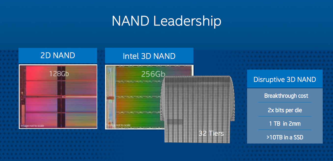
Intel claims that its 3D NAND is the most cost effective on the market and bases this on the fact that its die is 256Gbit whereas Samsung's is only up to 128Gbit at the moment. I'm not sure if I buy Intel's claim because while it's true that a higher capacity die results in higher array efficiency (i.e. peripheral circuitry takes less area), Samsung consciously went from a 24-layer 128Gbit MLC die to a 32-layer 86Gbit MLC die. In other words, Samsung could have upped the die capacity to ~170Gbit by just adding the extra layers, but the company chose to go with a smaller die instead. Smaller capacity dies have advantages in performance (higher parallelism) and applicability because eMMC/microSD devices have very strict die size constraints, so that might be a part of the reason why Samsung's strategy is so different from Intel's and Micron's. 
NAND Die Size
As the graph above shows, Intel's/Micron's NAND dies have historically been larger than the competitors', so the die capacity alone isn't enough to dictate whether Intel's 3D NAND is more cost efficient than Samsung, especially because both have 32 layers. Unlike Samsung, Intel didn't reveal the lithography that is used to manufacture the 3D NAND, but I would say it's safe to assume that the lithography is in the order of 30nm or 40nm because the whole idea of 3D NAND is to move away from multi-patterning to cut costs and with today's technology the smallest pitch of single-patterning is somewhere between 30nm and 40nm. Either way, it will be very interesting to see how Intel's 3D NAND stacks up against Samsung's because there are also some structural differences that affect the production cost as well as performance and endurance, but I'll save the structural analysis for a future article.
Intel said that 3D NAND technology will enable +10TB SSDs in the 'next couple of years', but it wasn't clear whether that is with first generation 3D NAND or some later generation with more layers and higher die capacity. Currently Intel's lineup tops out at 2TB (P3700 & P3600) with a 128Gbit die, so the 256Gbit die alone isn't enough to bring the capacities above 10TB. With effective controller development it should certainly be possible to build a 10TB SSD with a 256Gbit die, although I'm still inclined to believe that Mr. Crooke was referring to second or third generation 3D NAND with his statement. 
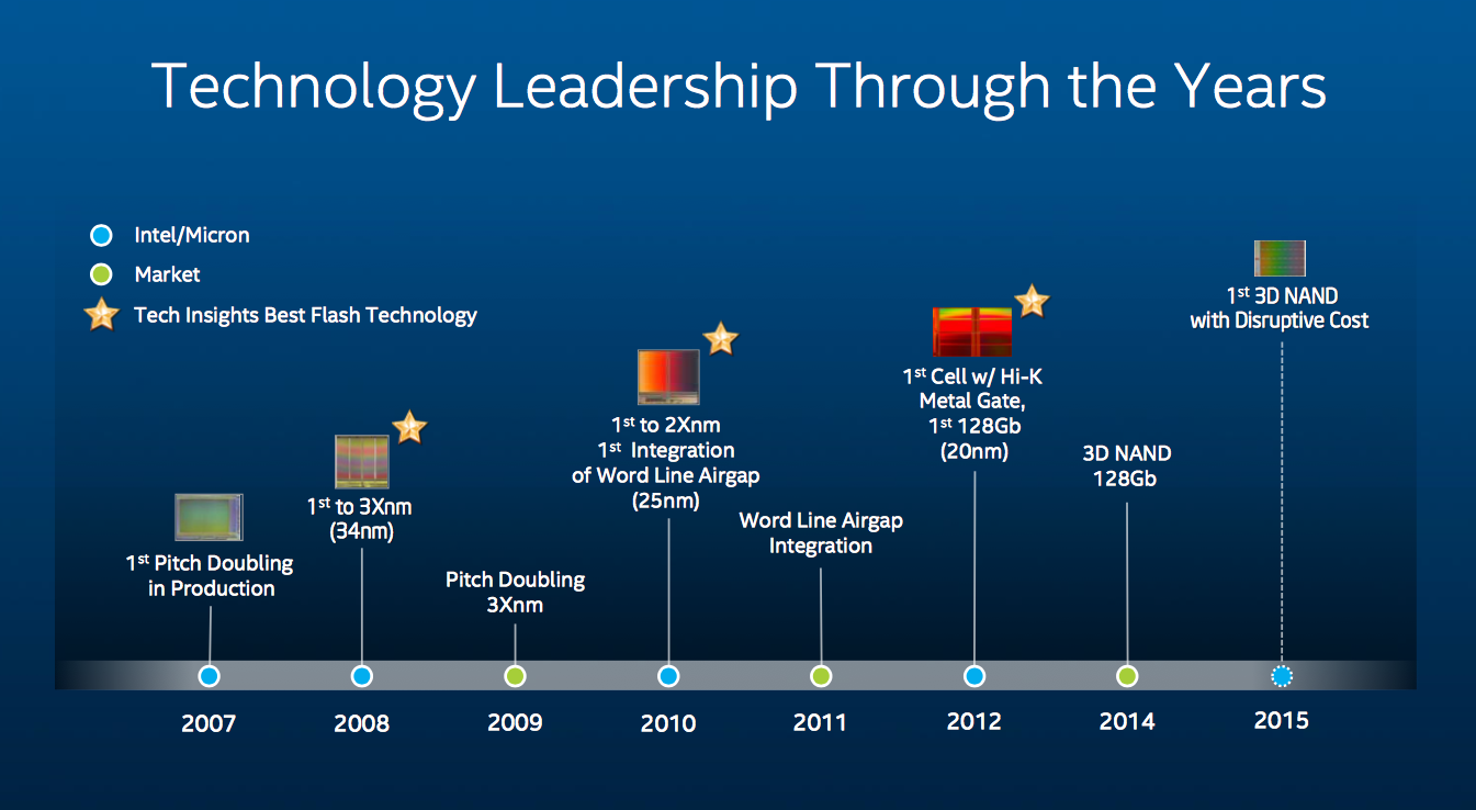
Similar to Intel's previous NAND efforts, 3D NAND has been jointly developed with Micron and will most likely be manufactured in the co-owned Utah plant as Intel sold its share in other fabs a couple of years ago. Interestingly enough, Mr. Crooke said that they also have the ability to bring 3D NAND production to an Intel fab, although to me that sounded more like a statement of technological possibility rather than a hint of future strategy. I wouldn't rule it out, though, but like Mr. Crooke said in the Q&A, Intel needs to have significant competitive advantage for it to make sense. In the past Intel's NAND technologies have generally been slightly ahead of the rest of the industry, but at least as of now Intel doesn't seem to have any substantial advantage in 3D NAND technology as Samsung is already shipping a 32-layer die and will likely ship a 48-layer die before Intel ships its 32-layer product.
All in all, we'll likely get more crumbs of information as the second half of 2015 gets closer. Given Intel's recent SSD strategy, I expect 3D NAND to first find its way to enterprise-class SSDs, but we'll see soon enough.

Friday, July 13, 2012

450-mm Fabs Ramp in 2017


The article below tries to project when the semiconductor industry will start building 450 mm wafer Fabs. A key point in the article is
"Gartner estimates that the total R&D cost of 450-mm tool development will cost about $17 billion cumulatively.... He noted that other estimates for the development cost differ widely, from about $10 billion at the low end to as much as $25 billion to $40 billion at the high end. "

The large size and range of the $10 to $40 billion cost  for tools development indicates that development will be slower than expected.

It will be interesting to see how Intel will use it to increase its lead in process technology (see Intel, ASML: Higher Performance/ Lower Cost Edge )


The high cost range for 450 mm tools development further confirms my points in the March blogs Moore's Law Slowwwing , and  Moore's Law End? (Next semiconductors gen. cost $10 billion)


Some interesting comments and summary of  IEEE Semiconductor Wafer Test Workshop 2012  by Ira Feldman

" By increasing the diameter of the wafer by 50% from 300 to 450 mm, the area will increase by 2.25x. And if the incremental cost for processing the larger wafer can be held to 12.5%, which may be achievable, the cost per area for the 450 mm wafer will be half that of the 300 mm. " ....

"The “elephant in the room” is how the semiconductor equipment manufacturers will recover their investment to develop the new equipment required to move to 450 mm. At this year’s SEMI Industry Strategy Symposium (ISS), Mike Splinter chairman and CEO of Applied Materials pointed out that the 300 mm wafer equipment had a total industry investment of $12 B which took fourteen years to recover. The current estimate is $15 to 20 B for the development of 450 mm equipment with an unknown time to recover. Obviously a topic of much “discussion” and “negotiation” between equipment suppliers and semiconductor fab operators – integrated device manufacturers (IDMs) and foundries alike."


Ron


First 450-mm fabs to ramp in 2017, says analyst

http://www.eetimes.com/electronics-news/4389918/First-450-mm-fabs-to-ramp-in-2017--says-analyst
Dylan McGrath

7/10/2012 12:59 AM EDT

SAN FRANCISCO—The first production semiconductor fabs to use 450-mm wafers are projected to commence operation in 2017, according to Christian Dieseldorff, a senior analyst with the fab tool vendor trade group SEMI's industry research and statistics group.


In a presentation at the Semicon West tradeshow here Monday (July 9), Dieseldorff predicted that three 450-mm fabs would commence operation in 2017. By that time, the total number of IC production fabs will have declined to 441, down from 464 this year, according to Dieseldorf.


Number of fabs beginning operation or in production in 2007 and estimates for 2017.


Several industry development projects are now focused on developing tools for 450-mm wafers, which leading edge chip makers want to transition to in order to increase the number of die per wafer, and thus profitability. Among these projects is the Global 450 Consortium, a $4.8 billion collaboration housed at the Albany NanoTech complex in New York and backed by semiconductor industry heavyweights Intel Corp., IBM Corp., Globalfoundries Inc., Samsung Electronics Co. Ltd. and Taiwan Semiconductor Manufacturing Co. Ltd. (TSMC).


Although the leading chip makers seem bent on moving to 450-mm wafers as quickly as possible, uncertainty remains about when development work will be completed and how many other chip vendors will follow their lead to larger wafers.


At the same event where Dieseldorff spoke Monday, Bob Johnson, research vice president for semiconductor manufacturing at Gartner Inc., said widespread adoption of 450-mm wafers would not occur until 2018 at the earliest, but more likely in 2019 or 2020.


Johnson predicted that the first alpha 450-mm development tools would be available late this year or early next year, with the first production tools not expected until 2016 or 2017. Johnson said there are a lot of predictions within the semiconductor industry about how difficult or easy the transition to 450-mm wafers will be, but that until people begin using 450-mm tools to process wafers, it is not possible to accurately predict how the larger wafers will react to the rigors of semiconductor manufacturing or how smoothly the transition will occur.


"You just don't know these things until you try them," Johnson said.


Johnson said that if the transition to 300-mm wafers in the early 2000s is any guide, chip makers would first construct large 450-mm fab shells but equip them sparsely while they "debugged" the process.


R&D investment estimates vary


Gartner estimates that the total R&D cost of 450-mm tool development will cost about $17 billion cumulatively, about $2 billion of which is being spent this year, Johnson said. He noted that other estimates for the development cost differ widely, from about $10 billion at the low end to as much as $25 billion to $40 billion at the high end.


"We aren't going to know what the [real] numbers are until we start getting some of these tools together and start putting them in production," Johnson said.


Johnson added that he believes the transition to 450-mm wafers is inevitable and predicted that the top 10 wafer fab equipment suppliers would contribute 80 percent of the R&D required to support the transition.


On Monday, Intel Corp. announced it planned to purchase a roughly 15 percent stake in leading lithography tool vendor ASML Holding NV as part of a $4.1 billion equity and R&D funding investment intended to accelerate the development of 450-mm capable tools and extreme ultraviolet (EUV) lithography. Also Monday, the Flemish Minister of Innovation, Ingrid Lieten, announced a commitment to invest in the building of clean room facilities for 450-mm diameter wafer processing at the IMEC research institute's pilot wafer fab in Leuven, Belgium.


Dieseldorff said SEMI estimates that total spending on front end chip fabs in 2012—including both fab construction and cost of equipment—will be between $59 billion and $60 billion, roughly flat with 2011. SEMI expects spending on front end fabs to grow 2 percent to 5 percent in 2013 to between $61 billion and $63 billion, he said.


SEMI estimates that total fab equipment spending, including discrete IC fabs, will total about $38.9 billion in 2012, roughly flat with 2011, Dieseldorff said. The trade group estimates that fab equipment spending will increase 20 percent in 2013 to $46.8 billion, he said.


Meanwhile, the estimated amount of spending on fab construction is expected to be slightly more than $6 billion in both 2012 and 2013, down from about $6.25 billion in 2011, Dieseldorff said. He added that the expectations for fab construction investment have increased in recent months with new projects announced by the likes of TSMC, Samsung, United Microelectronics Corp. (UMC), Semiconductor Manufacturing International Corp. (SMIC) and others. "The outlook for construction spending has improved dramatically" from previous estimates of double-digit declines, he said.


Despite pressure on the Japanese semiconductor industry in recent years, Japan continues to have more chip fabs than any other region, Dieseldorff said. By 2017, the total number of chips fabs in Japan is projected to decline to 105, down from 152 in 2007, Dieseldorff said. The number of fabs located in the Americas, which has the second highest number of fabs of all regions, is forecast to fall to 95 in 2017, down from 123 in 2007, he said.