A teardown of a new iPad reveals a shrunk SoC die (see below). In second half of 2011 an iPad's processor was made in the 45nm manufacturing process, while the current iPad seems to use a 32nm process.
The new 32nm A5 has a chip die area of only 69mm2 while in the 45nm process it was more than 120mm2 . I predicted that Apple will shift soon to 32nm process to improve battery life on March 22 in my blog post
New iPad-Teardown: Why Apple's A5X uses 45nm
This shrink will substantially reduce the cost of the A5 for Apple as Samsung improve the die yield of its 32nm high-k + metal gate LP manufacturing process.
Ron Maltiel
The iPad 2,4 Review: 32nm Brings Better Battery Life
by Anand Lal Shimpi on 5/4/2012 12:50:00 AM
http://www.anandtech.com/show/5789/the-ipad-24-review-32nm-a5-tested
When Apple launched the 3rd generation iPad (as the new iPad), it also dropped the price of the entry-level 16GB WiFi iPad 2 to $399. Apple's products tend to hold their values exceptionally well, so this two-tablet strategy made sense. Apple also proved the success of discount-the-previous-gen strategy with its iPhone line, where you can now buy current, n-1 and n-2 generations of iPhones at prices separated by $100.
What's different with the $399 iPad 2 is that Apple used it as a vehicle to introduce a new hardware platform, or more specifically, a new SoC.
When Apple launched the 3rd generation iPad (as the new iPad), it also dropped the price of the entry-level 16GB WiFi iPad 2 to $399. Apple's products tend to hold their values exceptionally well, so this two-tablet strategy made sense. Apple also proved the success of discount-the-previous-gen strategy with its iPhone line, where you can now buy current, n-1 and n-2 generations of iPhones at prices separated by $100.
What's different with the $399 iPad 2 is that Apple used it as a vehicle to introduce a new hardware platform, or more specifically, a new SoC.
The 32nm HK+MG Apple A5 SoC
Prior to the new iPad announcement there were three versions of the iPad 2:
iPad 2,1 iPad 2,2 iPad 2,3 iPad 2,4
A5 SoC 45nm LP 45nm LP 45nm LP 32nm LP
Connectivity WiFi WiFi + GSM WiFi + CDMA WiFi
Connectivity WiFi WiFi + GSM WiFi + CDMA WiFi
The 2,1 was WiFi-only, the 2,2 was GSM and the 2,3 was CDMA. The new addition to the family is the iPad 2,4. The 2,4 replaces the original iPad 2,1. It's also only available in a single capacity.
There's no known way to tell whether you're getting an iPad 2,4 vs. the older iPad 2,1 without opening the box. The 2,4 unit I ended up with was made in China, ruling out manufacturing region as a way of telling. The external box looks identical, as does the device itself.
The newer iPad 2,4 units should come with iOS 5.1 preloaded, while any older iPad 2,1 stock may have 5.0.1 or older. But the most accurate way to tell is by looking at what a utility like Geekbench will tell you about the hardware:
This particular iPad 2,4 sample came from Best Buy, and several attempts to find one elsewhere came up short. All indications seem to point to the iPad 2,4 being relatively rare, which makes sense considering what's inside it.
Although the iPad 2,1 and its 3G brethren all used a 45nm Apple A5 SoC, the iPad 2,4 uses a die-shrunk 32nm version. The performance remains the same, but the die is much smaller. This isn't however just a normal die shrink, as Apple is using Samsung's 32nm high-k + metal gate LP transistors for this new A5 die. Intel was first to make the HK+MG transition back at 45nm in 2007 and correctly predicted that no one else would make the move until 32nm at the earliest.
Transistors are amazingly complex to fully understand, but at a high level they're quite simple. Imagine a transistor as a silicon based switch. When on, current flows, and when off, current stops flowing. The smaller you make a transistor, the more likely it is to misbehave. If current flows while the transistor is off, you waste power. This is known as leakage current and can come from a number of sources.
One such source is the gate oxide/gate dielectric, a particularly thin part of modern day transistors - on the order of a handful of atoms thick. Thinning the gate dielectric is desirable up to a certain point, after which the dielectric simply leaks too much power. Switching to a different material here, specifically one with a higher dielectric constant (a higher k-value), can significantly reduce leakage current and mitigate this issue. This is exactly what the first part of Samsung's 32nm high-k + metal gate process does.
The second half of the new process is the introduction of a metal gate electrode. Switching from a polysilicon to a metal gate electrode results in higher drive current by elimination of a region of depleted conducting carriers between the gate electrode and gate dielectric.
The combination of these two innovations results in less wasted current and more efficient current delivery, which in turn can give us a more power efficient chip. It's a net win. It makes manufacturing more complex, and there's definitely a learning curve to implementing it, but after you get over that hurdle it becomes just another part of the process.
The More Cost Effective Die
Traditionally the move to a smaller process node brings about an increase in transistor density. As transistors get smaller, you can fit more of them into the same space (or the same number into a smaller space). It's this basic principle that makes Moore's Law work. If you can keep shrinking transistor size by about 50% every two years, you'll theoretically be able to double transistor count at the same cost every two years (or cut cost in half every two years). In practice it doesn't work this well. Newer processes are always more expensive than their predecessors initially and logic scaling is never perfect.
It's rare these days that we actually see a pure die shrink anymore. With Intel's tick-tock model we almost always see increases in functionality to accompany each process node shift. In the case of Ivy Bridge, we actually saw a significant increase in transistor count thanks to an improved GPU. With Apple's 32nm A5 however, we truly end up with a die shrunk version of the 45nm A5 SoC. About the only part of the computing world where we see these pure shrinks is in the console space where performance doesn't have to go up within a generation, but cost must go down.
 |
45nm A5 (left) vs. 32nm A5 (right) - Source: Chipworks
|
The original 45nm A5's die measured approximately 122mm^2. The new 32nm A5 has a surface area of only 69mm^2. That's actually amazingly good scaling at 57% of the old die size, as perfect scaling from 45nm to 32nm would be around 50.5%.
 |
| Die size comparison |
Assuming Apple could make full use of a 300mm wafer (which it can't, wafers are round, chips are rectangular at best so there are some unusable chips), Samsung could deliver 579 45nm A5 die to Apple. The move to 32nm would give Apple 75% more die per wafer at 1015 chips. Again both of these numbers are over estimates as they assume full usage of the surface area of a wafer as well as 100% yields, but you can see the benefit of a smaller die. As long as wafer costs increase by a factor less than the 75% increase in number of die per wafer, Apple can effectively reduce SoC cost by going this route.
These ARM based SoCs are already fairly cheap - all selling well below $30 (many around $15) - so there's not a whole lot of cost savings here. On a product like the $399 iPad 2, where Apple needs to do its best to maintain margins while holding onto (and growing) market share, every last dollar matters.
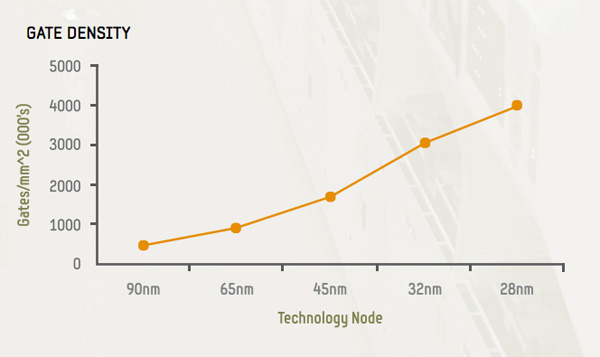 |
| Gate density vs. process node at Samsung |
There's another motivation for Apple however. Just as with any good microprocessor company, its best to introduce a new process technology on a known architecture. It's also a good idea to introduce a new process technology on lower volume products. The combination of both of these minimize risk. Should there be something wrong with the new process, introducing a new architecture on it just means you now have two very complex things to debug - the process technology and the chip's architecture. Should the new process not yield very well initially, you'd be similarly screwed if you were depending on it for your highest volume parts.
 |
32nm A5 in iPad 2,4 (Source: Chipworks)
|
Apple decided to try out Samsung's 32nm HK+MG process on the A5 used in the 3rd generation Apple TV and some of the new iPad 2s. The former is a relatively low volume product for Apple, while the latter still moves in significant quantities. To deal with that fact, Apple is continuing to ship the original 45nm iPad 2,1 alongside the new 32nm iPad 2,4. Any hiccups in Samsung's production of the A5 and there are still more than enough iPad 2,1s to go around. The risk of moving to 32nm is effectively mitigated, while the learnings Apple gains from building the 32nm A5 will pay off later this year as Apple ramps up production of a 32nm SoC for use in the next iPhone. It's a very smart strategy, one you would expect from an experienced chip company - not a device vendor. When you consider that Apple employs chip architects who have worked on everything from the Athlon 64 to the Cortex A15, Apple's behavior is no longer that surprising.
Apple gets two benefits from the iPad 2,4: lower manufacturing costs, and experience with Samsung's 32nm HK+MG process which it will later use in much greater volumes. What about customers who end up with an iPad 2,4? Better battery life and cooler operation, of course.
 |
| Impact of HK+MG at Samsung |
Remember the basics of Samsung's 32nm HK+MG process: a 40% performance improvement at the same leakage, or a 10x reduction in leakage at the same switching speed. As the iPad 2,4 retains the same clocks as the initial iPad 2, the benefit realized is a significant reduction in leakage current. This translates to tangibly better battery life.
Significant Battery Life Improvements details at
http://www.anandtech.com/show/5789/the-ipad-24-review-32nm-a5-tested/2
.....
Final Words
If Apple's A5 is any indication, Samsung's 32nm HK+MG process is extremely capable. Assuming Apple didn't change any fundamentals of its microarchitecture, the iPad 2,4's gains in battery life can be attributed directly to the process. The gains themselves are significant. We measured a 15% increase in our web browsing battery life, a nearly 30% increase in gaming battery life and an 18% increase in video playback battery life. Although Apple hasn't revised its battery life specs, the iPad 2,4 definitely lasts longer on a single charge than the original iPad 2.
If you're in the market for an iPad 2, the 2,4 is clearly the one to get - if you can find one that is. Unfortunately there's no sure fire way to tell that you're getting a 2,4 without opening the box and turning on the tablet, and I suspect most stores will get a bit irate if you're constantly buying and returning iPad 2s in search for a 32nm model. Presumably over time more of the available inventory will shift to 2,4 models, but based on our experiences in trying to find a 2,4 it's still pretty tough.
I would like to applaud Apple's 32nm migration plan. By starting with lower volume products and even then, only on a portion of the iPad 2s available on the market, Apple maintains a low profile and gets great experience with Samsung's 32nm HK+MG process. It's very clear that this is all in preparation for the next iPhone, which will almost certainly use Samsung's 32nm process and require it in significant volumes. It's obvious that Apple employs some very smart chip heads in Cupertino.
What I'd really like to see is a 32nm version of the A5X used in the new iPad. I don't know that there's much reason for that this year, especially when the 4th generation iPad will likely ship in the first half of 2013 with yet another new SoC (dual-core A15 + Rogue anyone?), but it'd still be nice to have. The power efficiency improvements are substantial and the 3rd gen iPad could definitely use them. Those of you who are waiting for the next iPhone should also be pretty happy about these results. Apple could easily deliver a higher clocked version of the A5 for the next iPhone while keeping power consumption equal to if not lower than where it's at today. The move to 32nm is going to be good all around it seems, and Samsung appears to be a very capable foundry partner for Apple. Despite all of the rumors of a rift in the relationship, the foundry side of things is working out well.
 Apple watch battery life is a key factor in how useful this new computer interface will be in our lives. Some information is discussed in the article below.


