Showing posts with label HKMG. Show all posts

Wednesday, December 2, 2015

Apple's iPhone, iPad Secret Sauce - Semiconductors

Apple over the last few years has leveraged its growing chip design knowledge to gain an added edge in performance and battery life. For example, the iPhone 6S Apple optimized the flash memory controller, which improves the speed of accessing flash data ( see iPhone 6s and iPhone 6s Results  and June 2012 blog Flash Memory Controller is the Secret Sauce )

Similarly, the latest Apple iPad pro which is using A9X SOC, also has some unique advantages (see below).


Additional information about the fabrication process used for A9 products at TSMC  is at
 - Apple A9 process fabricated using TSMC’s 16 nm finFET process. The A9 is fabricated using an 12 metal (11-Cu, 1-Al), 16 nm finFET CMOS process. The device features approximately 33 nm long metal gate finFET transistors having a 90 nm minimum contacted gate pitch; the same as used by their 20 nm HKMG process released in the summer of 2015.


Ron
Insightful, timely, and accurate semiconductor consulting.
Semiconductor information and news at - http://www.maltiel-consulting.com/


More on Apple’s A9X SoC: 147mm2@TSMC, 12 GPU Cores, No L3 Cache

Over the Thanksgiving break the intrepid crew over at Chipworks sent over their initial teardown information for Apple’s A9X SoC. The heart of the recently launched iPad Pro, the A9X is the latest iteration in Apple’s line of tablet-focused SoCs. We took an initial look at A9X last month, but at the time we only had limited information based on what our software tools could tell us. The other half of the picture (and in a literal sense, the entire picture) is looking at the physical layout of the chip, and now thanks to Chipworks we have that in hand and can confirm and reject some of our earlier theories.
A9X is the first dedicated ARM tablet SoC to be released on a leading-edge FinFET process, and it’s being paired with Apple’s first large-format tablet, which in some ways changes the rules of the game. Apple has to contend with the realities of manufacturing a larger SoC on a leading-edge process, and on the other hand a larger tablet that’s approaching the size of an Ultrabook opens up new doors as far as space and thermals are concerned. As a result while we could make some initial educated guesses, we’ve known that there would be a curveball in A9X’s design, and that’s something we couldn’t confirm until the release of Chipworks’ die shot. So without further ado:
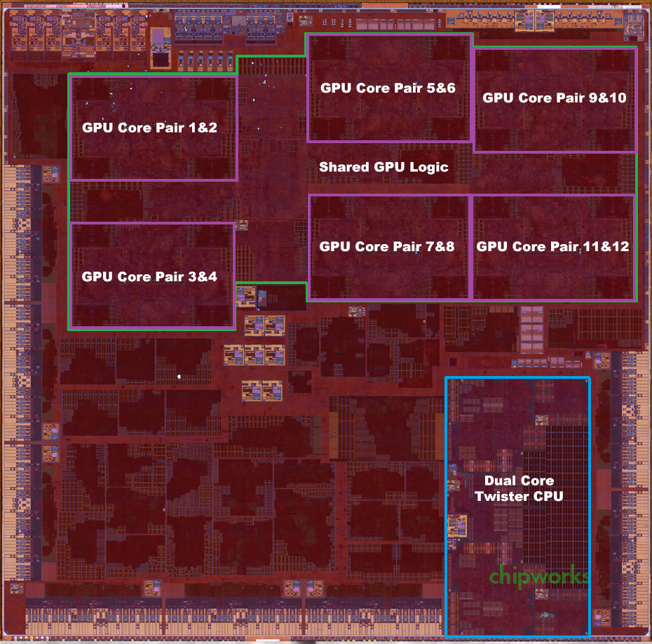
A9X Die Shot w/AT Annotations (Die Shot Courtesy Chipworks)
Apple SoC Comparison
A9XA9A8XA6X
CPU2x Twister2x Twister3x Typhoon2x Swift
CPU Clockspeed2.26GHz1.85GHz1.5GHz1.3GHz
GPUPVR 12 Cluster Series7PVR GT7600Apple/PVR GXA6850PVR SGX554 MP4
RAM4GB LPDDR42GB LPDDR42GB LPDDR31GB LPDDR2
Memory Bus Width128-bit64-bit128-bit128-bit
Memory Bandwidth51.2GB/sec25.6GB/sec25.6GB/sec17.1GB/sec
L2 Cache3MB3MB2MB1MB
L3 CacheNone4MB4MBN/A
Manufacturing ProcessTSMC 16nm FinFETTSMC 16nm &
Samsung 14nm
TSMC 20nmSamsung 32nm

Die Size: 147mm2, Manufactured By TSMC


First off, Chipworks’ analysis shows that the A9X is roughly 147mm2 in die size, and that it’s manufactured by TSMC on their 16nm FinFET process. We should note that Chipworks has only looked at the one sample, but unlike the iPhone 6s there’s no reason to expect that Apple is dual-sourcing a much lower volume tablet SoC.
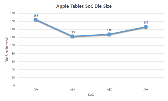
At 147mmthe A9X is the second-largest of Apple’s X-series tablet SoCs. Only the A5X, the first such SoC, was larger. Fittingly, it was also built relative to Apple’s equally large A5 phone SoC. With only 3 previous tablet SoCs to use as a point of comparison I’m not sure there’s really a sweet spot we can say that Apple likes to stick to, but after two generations of SoCs in the 120mm2 to 130mm2 range, A9X is noticeably larger.
Some of that comes from the fact that A9 itself is a bit larger than normal – the TSMC version is 104.5mm2 – but Apple has also clearly added a fair bit to the SoC. The wildcard here is what yields look like for Apple, as that would tell us a lot about whether 147mm2 is simply a large part or if Apple has taken a greater amount of risk than usual here. As 16nm FinFET is TSMC’s first-generation FinFET process, and save possibly some FPGAs this is the largest 16nm chip we know to be in mass production there, it’s reasonable to assume that yields aren’t quite as good as with past Apple tablet SoCs. But whether they’re significantly worse – and if this had any impact on Apple’s decision to only ship A9X with the more expensive iPad Pro – is a matter that we’ll have to leave to speculation at this time.
Finally, it's also worth noting just how large A9X is compared to other high performance processors. Intel's latest-generation Skylake processors measure in at ~99mm2 for the 2 core GT2 configuration (Skylake-Y 2+2), and even the 4 core desktop GT2 configuration (Intel Skylake-K 4+2) is only 122mm2. So A9X is larger than either of these CPU cores, though admittedly as a whole SoC A9X contains a number of functional units either not present on Skylake or on Skylake's Platform Controller Hub (PCH). Still, this is the first time that we've seen an Apple launch a tablet SoC larger than an Intel 4 core desktop CPU.

GPU: PVR 12 cluster Series7

One thing we do know is that Apple has invested a lot of their die space into ramping up the graphics subsystem and the memory subsystem that feeds it. Based on our original benchmark results of the A9X and the premium on FinFET production at the moment, I expected that the curveball with A9X would be that Apple went with a more unusual 10 core PowerVR Series7 configuration, up from 6 cores in A9. Instead, based on Chipworks’ die shot, I have once again underestimated Apple’s willingness to quickly ramp up the number of GPU cores they use. Chipworks’ shot makes it clear that there are 12 GPU cores, twice the number found in the A9.
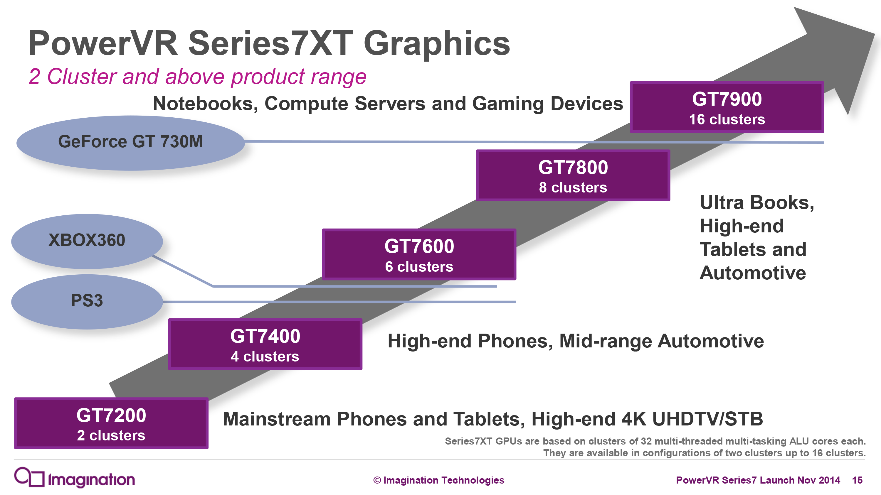
In Imagination’s PowerVR Series7 roadmap, the company doesn’t have an official name for a 12 core configuration, as this falls between the 8 core GT7800 and 16 core GT7900. So for the moment I’m simply calling it a “PowerVR 12 cluster Series7 design,” and with any luck Imagination will use a more fine-grained naming scheme for future generations of PowerVR graphics.
In any case, the use of a 12 core design is a bit surprising since it means that Apple was willing to take the die space hit to implement additional GPU cores, despite the impact this would have on chip yields and costs. If anything, with the larger thermal capacity and battery of the iPad Pro, I had expected Apple to use higher GPU clockspeeds (and eat the power cost) in order to save on chip costs. Instead what we’re seeing is a GPU that essentially offers twice the GPU power of A9’s GPU. We don’t know the clockspeed of the GPU – this being somewhat problematic to determine within the iOS sandbox – but based on our earlier performance results it’s likely that A9X’s GPU is only clocked slightly higher than A9’s. I say slightly higher because no GPU gets 100% performance scaling with additional cores, and with our GFXBench Manhattan scores being almost perfectly double that of A9’s, it stands to reason that Apple had to add a bit more to the GPU clockspeed to get there.
Meanwhile looking at the die shot a bit deeper, it’s interesting how spread out the GPU is. Apple needed to place 6 clusters and their associated shared logic on A9X, and they did so in a decidedly non-symmetrical manner. On that note, it’s worth pointing out that while Apple doesn’t talk about their chip design and licensing process, it’s highly likely that Apple has been doing their own layout/synthesis work for their PowerVR GPUs since at least the A4 and its PowerVR SGX 535, as opposed to using the hard macros from Imagination. This is why Apple is able to come up with GPU configurations that are supported by the PowerVR Rogue architecture, but aren’t official configurations offered by Imagination. A8X remains an especially memorable case since we didn’t initially know Series6XT could scale to 8 GPU cores until Apple went and did it, but otherwise what we see with any of these recent Apple SoCs is what should be a distinctly Apple GPU layout.
Moving on, the memory controller of the A9X is a 128-bit LPDDR4 configuration. With twice as many GPU cores, Apple needs twice as much memory bandwidth to maintain the same bandwidth-to-core ratio, so like the past X-series tablet SoCs, A9X implements a 128-bit bus. For Apple this means they now have a sizable 51.2GB/sec of memory bandwidth to play with. For a SoC this is a huge amount of bandwidth, but at the same time it’s quickly going to be consumed by those 12 GPU cores.

L3 Cache: None

Finally let’s talk about the most surprising aspect of the A9X, its L3 cache layout. When we published our initial A9X results we held off talking about the L3 cache as our tools pointed out some extremely unusual results that we wanted to wait on the Chipworks die shot to confirm. What we were seeing was that there wasn’t a section of roughly 50ns memory latency around the 4MB mark, which in A9 is the transfer size at which we hit its 4MB L3 victim cache.
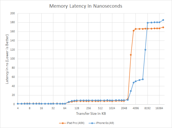
What Chipworks’ die shot now lets us confirm is that this wasn’t a fluke in our tools or the consequence of a change in how Apple’s L3 cache mechanism worked, but rather that there isn’t any L3 cache at all. After introducing the L3 cache with the A7 in 2013, Apple has eliminated it from the A9X entirely. The only cache to be found on A9X are the L1 and L2 caches for the CPU and GPU respectively, along with some even smaller amounts for cache for various other functional blocks.
The big question right now is why Apple would do this. Our traditional wisdom here is that the L3 cache was put in place to service both the CPU and GPU, but especially the GPU. Graphics rendering is a memory bandwidth-intensive operation, and as Apple has consistently been well ahead of many of the other ARM SoC designers in GPU performance, they have been running headlong into the performance limitations imposed by narrow mobile memory interfaces. An L3 cache, in turn, would alleviate some of that memory pressure and keep both CPU and GPU performance up.
One explanation may be that Apple deemed the L3 cache no longer necessary with the A9X’s 128-bit LPDDR4 memory bus; that 51.2GB/sec of bandwidth meant that they no longer needed the cache to avoid GPU stalls. However while the use of LPDDR4 may be a factor, Apple’s ratio of bandwidth-to-GPU cores of roughly 4.26GB/sec-to-1 core is identical to A9’s, which does have an L3 cache. With A9X being a larger A9 in so many ways, this alone isn’t the whole story.
What’s especially curious is that the L3 cache on the A9 wasn’t costing Apple much in the way of space. Chipworks puts the size of A9’s 4MB L3 cache block at a puny ~4.5 mm2, which is just 3% the size of A9X. So although there is a cost to adding L3 cache, unless there are issues we can’t see even with a die shot (e.g. routing), Apple didn’t save much by getting rid of the L3 cache.
Our own Andrei Frumusanu suspects that it may be a power matter, and that Apple was using the L3 cache to save on power-expensive memory operations on the A9. With A9X however, it’s a tablet SoC that doesn’t face the same power restrictions, and as a result doesn’t need a power-saving cache. This would be coupled with the fact that with double the GPU cores, there would be a lot more pressure on just a 4MB cache versus the pressure created by A9, which in turn may drive the need for a larger cache and ultimately an even larger die size.
As it stands there’s no one obvious reason, and it’s likely that all 3 factors – die size, LPDDR4, and power needs – all played a part here, with only those within the halls of One Infinite Loop knowing for sure. However I will add that since Apple has removed the L3 cache, the GPU L2 cache must be sizable. Imagination’s tile based deferred rendering technology needs an on-chip cache to hold tiles in to work on, and while they don’t need an entire frame’s worth of cache (which on iPad Pro would be over 21MB), they do need enough cache to hold a single tile. It’s much harder to estimate GPU L2 cache size from a die shot (especially with Apple’s asymmetrical design), but I wouldn’t be surprised of A9X’s GPU L2 cache is greater than A9’s or A8X’s.
In any case, the fact that A9X lacks an L3 cache doesn’t change the chart-topping performance we’ve been seeing from iPad Pro, but it means that Apple has once more found a way to throw us a new curveball. And closing on that note, we’ll be back in December with our full review of the iPad Pro and a deeper look at A9X’s performance, so be sure to stay tuned for that.

Friday, January 23, 2015

Apple Watch battery life, A5-caliber CPU inside

Apple watch battery life is a key factor in how useful this new computer interface will be in our lives. Some information is discussed in the article below. 
"Apple opted to use a relatively powerful processor and high-quality screen for the Apple Watch, both of which contribute to significant power drain. Running a stripped-down version of iOS codenamed SkiHill, the Apple S1 chip inside the Apple Watch is surprisingly close in performance to the version of Apple's A5 processor found inside the current-generation iPod touch,"

More about A5 power consumption is in May 2012 article Apple's A5 Die Shrink, Improve Battery Life, Cut Cost .


 Ron
Insightful, timely, and accurate semiconductor consulting.
Semiconductor information and news at - 
http://www.maltiel-consulting.com/


Apple targets for Apple Watch battery life revealed, A5-caliber CPU inside


Although Apple has said that the Apple Watch will need to be charged nightly, the company has not disclosed any details on how long the wearable's battery will last. For the first time, people with knowledge of the Apple Watch's development have provided us with the specific performance targets Apple wants to achieve for the Apple Watch battery, but the actual numbers may fall short of those targets.

According to our sources, Apple opted to use a relatively powerful processor and high-quality screen for the Apple Watch, both of which contribute to significant power drain. Running a stripped-down version of iOS codenamed SkiHill, the Apple S1 chip inside the Apple Watch is surprisingly close in performance to the version of Apple's A5 processor found inside the current-generation iPod touch, while the Retina-class color display is capable of updating at a fluid 60 frames per second.
Apple initially wanted the Apple Watch battery to provide roughly one full day of usage, mixing a comparatively small amount of active use with a larger amount of passive use. As of 2014, Apple wanted the Watch to provide roughly 2.5 to 4 hours of active application use versus 19 hours of combined active/passive use, 3 days of pure standby time, or 4 days if left in a sleeping mode. Sources, however, say that Apple will only likely achieve approximately 2-3 days in either the standby or low-power modes…

Apple has also been stress-testing the Apple Watch's battery life with pre-bundled and third-party applications. Our sources say that Apple is targeting 2.5 hours of "heavy" application use, such as processor-intensive gameplay, or 3.5 hours of standard app use. Interestingly, Apple expects to see better battery life when using the Watch's fitness tracking software, which is targeted for nearly 4 hours of straight exercise tracking on a single charge.

As Apple is positioning the Apple Watch as a timepiece, the company has conducted numerous tests to determine how long it can run purely in time-keeping modes. We're told that the Watch should be able to display its clock face for approximately three hours, including watch ticking animations, if nothing else is done with the device. However, it's unlikely that most people would actually keep the Apple Watch clock face turned on for even three hours straight in a single day. When the Watch screen is not in use, the display is powered off, and the clock demands much less energy.

Considered separately, the active use app, clock, and fitness numbers sound very low, but the reality is that people will passively wear the Apple Watch for most of the day, actively interacting with it only for short periods of time. That's why the Watch will be able to last the average user roughly a day on a single charge. We're told that Apple has been shooting for roughly 19 hours of mixed usage each day, but that the company may not hit that number in the first generation version.

Sources tell us that battery life has remained a source of concern for Apple over the past year, and was a contributing factor for Apple pushing back the retail launch from an originally planned late 2014 to early 2015. To test real-world performance in a variety of conditions, the company has circulated a surprisingly large number of test units of the Watch: nearly 3,000 are said to be currently roaming around, mostly the stainless steel variant.
Apple has also been working to perfect the MagSafe-based inductive charging mechanism for the Watch, which sources indicate was responsible for slower-than-expected recharging times that hopefully will be fixed in time for the product's release. The company has developed both plastic and stainless steel versions of the circular charger, potentially one for the $349 aluminum and plastic Apple Watch Sport, and the other for the higher-end models. It's unclear at this point whether the company will sell multiple versions of the charger, as Apple has only shown the metal variant, though the Apple Watch Edition is said to ship with a special box and charging dock that may incorporate the stainless steel MagSafe connector.

As of earlier this month, the Apple Watch is on track to ship by the end of March. We previously detailed how the Watch will integrate with the iPhone via an iOS 8.2-based Companion application.

Thursday, December 13, 2012

Apple iPad 4 – A6X Tear-down

Chipwork's teardown of the new Apple iPad 4 reveals a major redesign of the graphic processor (GPU). The much larger area dedicated to the GPU and wider interface of the DRAM improves the display and touch screen performance of the iPad 4. It probably also helps prolong battery life.


" The A6 is 94mm2 while the A6X is 123mm2 – a full 30% larger.So where did that extra area go? Well, firstly, it did not go to the CPU core. The A6X uses the identical CPU to the A6. Same size, same layout. This is not surprising given that the prior CPU used custom layout techniques, and therefore it would be a huge amount of work to redesign so soon. Much of the extra area has gone to the GPU cores which are up from 3 to 4. More notable is that each of these GPU cores is much larger.On the A6X each GPU core is 8.7mm2 while the A6 GPU cores are only 5.4mm2. The overall area occupied by the A6X GPU cores is more than double that of the A6!

So we see that of the 29 mm2 of new area on the A6X, a full 18.6 mm2 is the result of the increased quantity of graphics processing. Impressive!

Additionally, if you look closely at the GPU cores (which our high magnification scopes allow us to do), we can see they are actually split into sub-cores themselves. Each GPU core is sub-divided into 9 sub-cores (2 sets of 4 identical sub-cores plus a central core). This could be done to allow for more efficient parallel processing, or to allow for a higher maximum clock rate. In either case, these GPUs should result in some blazing graphics on your iPad.

Other items of note:

It looks like the A6X has double the SDRAM interface width of the A6 (again likely to allow for greater graphics processing power).

Other than the CPU, it appears all the other digital cores have new layouts. This chip is not just a minor tweak from the A6, a lot of work has gone into this.

Apple has reduced the number of core PLLs needed from 9 on the A6 to 8 on the A6X. However they have moved them close to the middle of the chip which may allow for better control over clock skew across the chip.

Many of the analog and interface cores have been reused from the A6, however there are also some new interface blocks."

Additional information

Ron Maltiel   www.maltiel-consulting.com

Monday, December 3, 2012

3D Flash NAND Devices and Process

The article below discusses developments in 3D Flash NAND. Toshiba and Macronix have different approaches. See more details about Toshiba Next NAND- 3D with 15 Layers.


Applied material discusses processing issues and new equipment to address them.

"According to Applied Materials, building 3D NAND structures in like trying to dig a one-kilometer-deep, three-kilometer-long trench with walls exactly three meters apart, through interleaved rock strata."

Ron Maltiel
www.maltiel-consulting.com


3D NAND flash is coming

http://www.edn.com/electronics-blogs/practical-chip-design/4401542/3D-NAND-flash-is-coming

Brian Bailey - November 15, 2012

Flash memory has very quickly risen from being an obscure memory type to perhaps becoming the dominant memory type for many devices, including music players, cell phones, tablets and now increasingly servers and mainstream PCs. But flash memory does not scale quite as well as the more traditional DRAM that it is replacing. It is thought that DRAM can scale down to 1nm whereas we are already hitting some problems with the scaling of the floating gate in NAND flash. It is not thought that planar NAND can go below 10nm which is only a couple of processes steps away from where we are today.


There are several other types of memory being developed, including spin-torque MRAM and Resistive RAM (ReRAM) that may replace both RAM and flash in the future. Another exciting direction is 3D NAND structures. In some respects this is similar to FinFET development for traditional transistors that are finding their way into 20nm and 14nm processes.


Toshiba is one company pushing 3D NAND processes with its p-BiCS (pipe-shaped Bit Cost Scalable) technology. The thought is that rather than lay the cells flat on the surface, higher densities can be achieved by stacking them on top of each other. This is shown diagrammatically in the figure below. As you can see this is not the same as 3D ICs where multiple substrates are layered on top of each other and connected using through silicon vias (TSV), this is building cells on top of each other to create U shaped bit lines. They currently have 16 layers devices where the hole size is 50nm and Toshiba says that the process becomes cheaper than the traditional NAND processes when more than 15 layers are created. Samples are expected next year and volume shipments by 2015...
  Additional details

Tuesday, October 30, 2012

Apple's A6X Processor 32nm Process Advantages

Apple's latest iPad 4 processor comes with its latest processor: an A6X, which Apple says delivers twice the CPU and graphics performance as the A5X. See below some details about Apple's A6X processor.

"Apple moved from a 45nm process to a more power-efficient 32nm process. Instead of keeping performance the same and decreasing the iPad's thickness and weight, Apple instead chose to double its performance without sacrificing all-day battery life."

More about Apple's optimizing process and design at iPhone A6 Teardown Update

Ron
http://www.maltiel-consulting.com/


Deducing details about Apple's A6X processor


Apple promises double the CPU and graphics performance over the A5X, but how?

by Chris Foresman - Oct 23 2012, 3:25pm PDT


As usual, Apple didn't share many specifics about its new A6 "Extreme" (A6X) processor, which powers the fourth-generation iPad. However, by looking at Apple's claims that it's "twice as fast" as the A5X-powered third-gen iPad, it may be possible to deduce what's inside.

According to Apple, the A6X processor "delivers up to twice the CPU and graphics performance of the A5X chip." In other words, the dual-core CPU can process data twice as fast as the dual-core 1GHz, Cortex A9-based A5X. It can also churn through OpenGL triangles and textures at twice the rate of the PowerVR SGX543MP4 in the A5X. So how did Apple do that?

Looking at CPU power for the moment, we already know that Apple designed a custom ARM-based core for the A6. Running at 1.2GHz in the iPhone 5, two A6 cores run twice as fast as two 800MHz A5 cores in an iPhone 4S.

However, the A5X in the third-gen iPad was clocked at 1GHz. That means Apple is clocking the A6X higher yet. Given that architectural improvements account for some of the speed increase, Apple only had to clock the iPhone 5 at 150 percent to achieve double the compute performance of the iPhone 4S. With this in mind, we believe Apple is clocking the A6X's CPU cores at 1.5GHz.

Examining the GPU is slightly different. Apple already jammed four SGX543 GPU cores into the A5X in order to achieve performance parity with the two SGX543 GPU cores in the A5 chip that powers the iPad 2. The extra GPUs were needed just to keep up with the 2048×1532 pixel Retina display, so these did not offer any graphics performance improvement. However, Apple says that the A6X pumps pixels twice as fast.

Apple could be using a newer-generation PowerVR core, but that appears to be very unlikely. Only one announced processor is known to use a PowerVR Series6 design, and it won't even begin sampling until 2013. Given that Apple just released the A6 a month ago, we're confident Apple is still using the same SGX543 core.

Here's what we know about the PowerVR SGX543 core's performance: it scales almost linearly with the number of cores and clock speed. So to double the performance, Apple would either have to double the number of cores to eight or double the clock speed of each of the four cores. Apple says that the A6X has "quad-core graphics"—the same as the A5X—so Apple clearly boosted the clock speed. Since the GPUs in the A5X were clocked at 250MHz, we believe that Apple has clocked the SGX543 cores at 500MHz.

Given the significant boosts in clock frequency—150 percent for the CPU cores, and 200 percent for the GPU cores—you may be wondering how Apple can still promise a 10-hour battery life. After all, the iPad still has the exact same 42.5Whr battery, but the processor is twice as powerful. The power savings come from the same place as we saw in the iPhone—Apple moved from a 45nm process to a more power-efficient 32nm process. Instead of keeping performance the same and decreasing the iPad's thickness and weight, Apple instead chose to double its performance without sacrificing all-day battery life.

Of course, we won't know how accurate our educated guesses are until one of the new iPads can be thoroughly benched, and the A6X's architecture is analyzed by the likes of Chipworks. However, we feel confident suggesting Apple has mated two A6 ARM cores running at 1.5GHz with four PowerVR SGX543 cores running at 500MHz. Given the performance results we saw with the iPhone 5, we expect the updated iPad will remain at the top of the tablet performance heap for some time.

Tuesday, October 16, 2012

Toshiba Next NAND- 3D with 15 Layers


The winner for the next flash memory approach is still not clear. A strong candidate is stacking memory NAND dies one on top of another. The dies are connected using Through Silicon Vias (TSV). Toshiba has a different approach to 3D " not stacking NAND chips one atop the other but rather stacking layers of NAND in a single chip" See more details below.

The key concern for next NAND generations is the 5 years lead time to build a new $5 billion fab, which could be designed for the wrong process technology.

It does not help that "the number of electrons in a gate decreases as the process geometry size is reduced....below 10nm the number of critical electrons in a gate can be as few as 10 – and that losing 10 electrons could seriously affect the gate's functioning. He says there are a variety of issues with such very small cells, such as bit-line loading, interference and leakage, leading to signal retention and reliability issues, for which, currently, there are no solutions.


These problems may make 10nm NAND technology impractical and sub-10nm impossible. Park suggests that 3D stacking, putting dies on on top of another, could be away out of this trap. He charts various approaches and identifies issues with each one, mentioning yield and retention as overall issues" (see more at Flashboys: HEELLLP, we're trapped in a process size shrink crunch)

Ron
www.maltiel-consulting.com


The 3D die stack tack: Toshiba builds towering column of flash


Resistance is futile
By Chris Mellor, 15th October 2012 09:28 GMT


Toshiba is building high rise flash and ReRAM chips, with prototypes coming next year and volume shipping in 2015.

The idea of high-rise or 3D chips is that we can sidestep limitations on increasing the storage density of flash or memory chips by stacking them one on top of the other, increasing the storage density on a Mbits/in 2 basis by building upwards, in the same way as high-rise housing increases the number of people living in the ground footprint of a block of flats.

Hot on the heels of our story about the NAND scaling trap [1], with 3D NAND and ReRAM suggested as two of the potential escape routes, we learn from Nikkei Electronics [2] that Toshiba is building 3D dies using a type of NAND, its p-BiCS (pipe-shaped Bit Cost Scalable) [3] technology, and also a coming replacement technology for NAND, ReRAM (Resistive RAM) which combines attributes of RAM and NAND to provide byte addressability, DRAM-class speed and NAND non-volatility.

As the slide below shows, 3D flash involves layers of NAND dies with communicating holes - TSVs or Through Silicon Vias - linking them to a stack controller at the base of the stack. It is not stacking NAND chips one atop the other but rather stacking layers of NAND in a single chip.


Toshiba p-BiCS technology [4]

Toshiba's p-BiCS NAND has a 50nm-size hole and 16 layers. Toshiba's chief engineer, Masaki Momodomi, at its Semiconductor & Storage Products Co., says that p-BiCS becomes cheaper than ordinary NAND when more than 15 layers are used, presumably comparing similar capacity levels. The company aims to deliver 128Gbit and 256Gbit prototype samples next year, engineering samples in 2014, with volume shipments in 2015; we are more than two years away from seeing product hit the streets.

The ReRAM [5] technology has a similar timescale though at lower capacities. It has much faster write times than NAND and Toshiba sees it fulfilling a different role from p-BiCS, being used closer to CPUs than p-BiCS, with STT-RAM being used for cache memories in, for example, SSDs. This is a similar hierarchy to the one proposed by Hynix in our NAND Scaling Trap story today. Jim Handy of Objective Analysis said; "It makes sense that ReRAM … would be used in performance applications, though. They are far faster at writes than NAND is, they are random access devices which NAND is not, and they don't need ECC. All this lends itself to faster performance."

Toshiba's ReRAM technology will appear in the same sequence of prototype samples, engineering samples and volume production as p-BiCS with the same general timing. A picture of a 64Gbit ReRAM device was shown at the Toshiba briefing attended by Nikkei Electronic but Toshiba intends to deliver generally equivalent p-BiCS and ReRAM capacities.

It is set of reducing the size of its current 1Xnm (19nm) NAND cells, and will target 1Ynm (18-14nm we understand) products this year and 1Znm (10-13nm) products next year.

Handy said: "All those new technologies (MRAM, ReRAM, FRAM...) perform better than NAND (BiCS is a kind of NAND) but are more costly. In memory cost is everything so these alternatives don't do well. The promise of these technologies is that they will move right past NAND's scaling limit. If they do that they will eventually become cheaper than NAND, but not until NAND has stopped scaling for 2 process generations.

"Toshiba talks about 1y and 1z, their processes after 19nm. I suspect that NAND will stop scaling at around 10nm, but BiCS will cause NAND pricing to continue to decline after that. Of course, those geniuses who have been coaxing NAND as far as 19nm could very well keep pulling rabbits out of their hats and push it well beyond 10nm - time will tell."

Will we see continued NAND process size decreases or 3D as the chosen way to get more capacity from a NAND die's footprint? Handy said: "The most recent ITRS [International Technology Roadmap for Semiconductors] [6] roadmap plots out two different directions for NAND - vertical (BiCS) and conventional. The industry really doesn't know where it's going to go, but it has plans in place for either eventuality."

Friday, May 4, 2012

Apple's A5 Die Shrink, Improve Battery Life, Cut Cost

A teardown of a new iPad reveals a shrunk SoC die (see below). In second  half of 2011 an iPad's processor was made in the 45nm manufacturing process, while the current iPad seems to use a 32nm process.

The new 32nm A5 has a chip die area of only 69mm2 while in the 45nm process it was more than 120mm2 . I predicted that Apple will shift soon to 32nm process to improve battery life on March 22 in my blog post  New iPad-Teardown: Why Apple's A5X uses 45nm

This shrink will substantially reduce the cost of the A5 for Apple as Samsung improve the die yield of its  32nm high-k + metal gate LP manufacturing process.


Ron Maltiel


The iPad 2,4 Review: 32nm Brings Better Battery Life


by Anand Lal Shimpi on 5/4/2012 12:50:00 AM
http://www.anandtech.com/show/5789/the-ipad-24-review-32nm-a5-tested

When Apple launched the 3rd generation iPad (as the new iPad), it also dropped the price of the entry-level 16GB WiFi iPad 2 to $399. Apple's products tend to hold their values exceptionally well, so this two-tablet strategy made sense. Apple also proved the success of discount-the-previous-gen strategy with its iPhone line, where you can now buy current, n-1 and n-2 generations of iPhones at prices separated by $100.

What's different with the $399 iPad 2 is that Apple used it as a vehicle to introduce a new hardware platform, or more specifically, a new SoC.


When Apple launched the 3rd generation iPad (as the new iPad), it also dropped the price of the entry-level 16GB WiFi iPad 2 to $399. Apple's products tend to hold their values exceptionally well, so this two-tablet strategy made sense. Apple also proved the success of discount-the-previous-gen strategy with its iPhone line, where you can now buy current, n-1 and n-2 generations of iPhones at prices separated by $100.

What's different with the $399 iPad 2 is that Apple used it as a vehicle to introduce a new hardware platform, or more specifically, a new SoC.


The 32nm HK+MG Apple A5 SoC

Prior to the new iPad announcement there were three versions of the iPad 2:


iPad 2,1 iPad 2,2 iPad 2,3 iPad 2,4

A5 SoC 45nm LP 45nm LP 45nm LP 32nm LP

Connectivity WiFi WiFi + GSM WiFi + CDMA WiFi


Connectivity WiFi WiFi + GSM WiFi + CDMA WiFi
The 2,1 was WiFi-only, the 2,2 was GSM and the 2,3 was CDMA. The new addition to the family is the iPad 2,4. The 2,4 replaces the original iPad 2,1. It's also only available in a single capacity.


There's no known way to tell whether you're getting an iPad 2,4 vs. the older iPad 2,1 without opening the box. The 2,4 unit I ended up with was made in China, ruling out manufacturing region as a way of telling. The external box looks identical, as does the device itself.

The newer iPad 2,4 units should come with iOS 5.1 preloaded, while any older iPad 2,1 stock may have 5.0.1 or older. But the most accurate way to tell is by looking at what a utility like Geekbench will tell you about the hardware:

This particular iPad 2,4 sample came from Best Buy, and several attempts to find one elsewhere came up short. All indications seem to point to the iPad 2,4 being relatively rare, which makes sense considering what's inside it.
Although the iPad 2,1 and its 3G brethren all used a 45nm Apple A5 SoC, the iPad 2,4 uses a die-shrunk 32nm version. The performance remains the same, but the die is much smaller. This isn't however just a normal die shrink, as Apple is using Samsung's 32nm high-k + metal gate LP transistors for this new A5 die. Intel was first to make the HK+MG transition back at 45nm in 2007 and correctly predicted that no one else would make the move until 32nm at the earliest.

Transistors are amazingly complex to fully understand, but at a high level they're quite simple. Imagine a transistor as a silicon based switch. When on, current flows, and when off, current stops flowing. The smaller you make a transistor, the more likely it is to misbehave. If current flows while the transistor is off, you waste power. This is known as leakage current and can come from a number of sources.


One such source is the gate oxide/gate dielectric, a particularly thin part of modern day transistors - on the order of a handful of atoms thick. Thinning the gate dielectric is desirable up to a certain point, after which the dielectric simply leaks too much power. Switching to a different material here, specifically one with a higher dielectric constant (a higher k-value), can significantly reduce leakage current and mitigate this issue. This is exactly what the first part of Samsung's 32nm high-k + metal gate process does.

The second half of the new process is the introduction of a metal gate electrode. Switching from a polysilicon to a metal gate electrode results in higher drive current by elimination of a region of depleted conducting carriers between the gate electrode and gate dielectric.


The combination of these two innovations results in less wasted current and more efficient current delivery, which in turn can give us a more power efficient chip. It's a net win. It makes manufacturing more complex, and there's definitely a learning curve to implementing it, but after you get over that hurdle it becomes just another part of the process.

The More Cost Effective Die

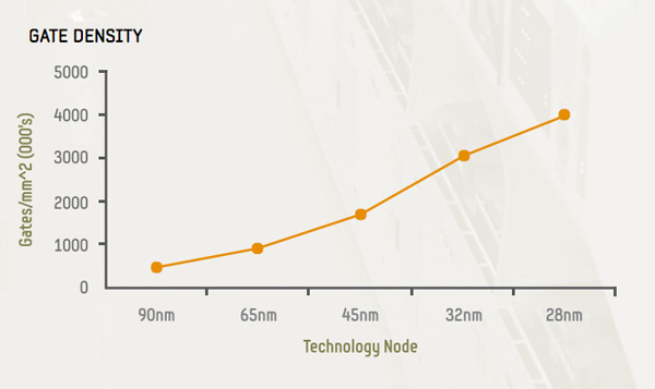
Traditionally the move to a smaller process node brings about an increase in transistor density. As transistors get smaller, you can fit more of them into the same space (or the same number into a smaller space). It's this basic principle that makes Moore's Law work. If you can keep shrinking transistor size by about 50% every two years, you'll theoretically be able to double transistor count at the same cost every two years (or cut cost in half every two years). In practice it doesn't work this well. Newer processes are always more expensive than their predecessors initially and logic scaling is never perfect.

It's rare these days that we actually see a pure die shrink anymore. With Intel's tick-tock model we almost always see increases in functionality to accompany each process node shift. In the case of Ivy Bridge, we actually saw a significant increase in transistor count thanks to an improved GPU. With Apple's 32nm A5 however, we truly end up with a die shrunk version of the 45nm A5 SoC. About the only part of the computing world where we see these pure shrinks is in the console space where performance doesn't have to go up within a generation, but cost must go down.


45nm A5 (left) vs. 32nm A5 (right)
45nm A5 (left) vs. 32nm A5 (right) - Source: Chipworks


 The original 45nm A5's die measured approximately 122mm^2. The new 32nm A5 has a surface area of only 69mm^2. That's actually amazingly good scaling at 57% of the old die size, as perfect scaling from 45nm to 32nm would be around 50.5%.


Die size comparison

Assuming Apple could make full use of a 300mm wafer (which it can't, wafers are round, chips are rectangular at best so there are some unusable chips), Samsung could deliver 579 45nm A5 die to Apple. The move to 32nm would give Apple 75% more die per wafer at 1015 chips. Again both of these numbers are over estimates as they assume full usage of the surface area of a wafer as well as 100% yields, but you can see the benefit of a smaller die. As long as wafer costs increase by a factor less than the 75% increase in number of die per wafer, Apple can effectively reduce SoC cost by going this route.

These ARM based SoCs are already fairly cheap - all selling well below $30 (many around $15) - so there's not a whole lot of cost savings here. On a product like the $399 iPad 2, where Apple needs to do its best to maintain margins while holding onto (and growing) market share, every last dollar matters.


Gate density vs. process node at Samsung

There's another motivation for Apple however. Just as with any good microprocessor company, its best to introduce a new process technology on a known architecture. It's also a good idea to introduce a new process technology on lower volume products. The combination of both of these minimize risk. Should there be something wrong with the new process, introducing a new architecture on it just means you now have two very complex things to debug - the process technology and the chip's architecture. Should the new process not yield very well initially, you'd be similarly screwed if you were depending on it for your highest volume parts.
32nm A5 in iPad 2,4 (Source: Chipworks)


Apple decided to try out Samsung's 32nm HK+MG process on the A5 used in the 3rd generation Apple TV and some of the new iPad 2s. The former is a relatively low volume product for Apple, while the latter still moves in significant quantities. To deal with that fact, Apple is continuing to ship the original 45nm iPad 2,1 alongside the new 32nm iPad 2,4. Any hiccups in Samsung's production of the A5 and there are still more than enough iPad 2,1s to go around. The risk of moving to 32nm is effectively mitigated, while the learnings Apple gains from building the 32nm A5 will pay off later this year as Apple ramps up production of a 32nm SoC for use in the next iPhone. It's a very smart strategy, one you would expect from an experienced chip company - not a device vendor. When you consider that Apple employs chip architects who have worked on everything from the Athlon 64 to the Cortex A15, Apple's behavior is no longer that surprising.


Apple gets two benefits from the iPad 2,4: lower manufacturing costs, and experience with Samsung's 32nm HK+MG process which it will later use in much greater volumes. What about customers who end up with an iPad 2,4? Better battery life and cooler operation, of course.


Impact of HK+MG at Samsung


Remember the basics of Samsung's 32nm HK+MG process: a 40% performance improvement at the same leakage, or a 10x reduction in leakage at the same switching speed. As the iPad 2,4 retains the same clocks as the initial iPad 2, the benefit realized is a significant reduction in leakage current. This translates to tangibly better battery life.


Significant Battery Life Improvements details at http://www.anandtech.com/show/5789/the-ipad-24-review-32nm-a5-tested/2
.....

Final Words

If Apple's A5 is any indication, Samsung's 32nm HK+MG process is extremely capable. Assuming Apple didn't change any fundamentals of its microarchitecture, the iPad 2,4's gains in battery life can be attributed directly to the process. The gains themselves are significant. We measured a 15% increase in our web browsing battery life, a nearly 30% increase in gaming battery life and an 18% increase in video playback battery life. Although Apple hasn't revised its battery life specs, the iPad 2,4 definitely lasts longer on a single charge than the original iPad 2.


If you're in the market for an iPad 2, the 2,4 is clearly the one to get - if you can find one that is. Unfortunately there's no sure fire way to tell that you're getting a 2,4 without opening the box and turning on the tablet, and I suspect most stores will get a bit irate if you're constantly buying and returning iPad 2s in search for a 32nm model. Presumably over time more of the available inventory will shift to 2,4 models, but based on our experiences in trying to find a 2,4 it's still pretty tough.


I would like to applaud Apple's 32nm migration plan. By starting with lower volume products and even then, only on a portion of the iPad 2s available on the market, Apple maintains a low profile and gets great experience with Samsung's 32nm HK+MG process. It's very clear that this is all in preparation for the next iPhone, which will almost certainly use Samsung's 32nm process and require it in significant volumes. It's obvious that Apple employs some very smart chip heads in Cupertino.


What I'd really like to see is a 32nm version of the A5X used in the new iPad. I don't know that there's much reason for that this year, especially when the 4th generation iPad will likely ship in the first half of 2013 with yet another new SoC (dual-core A15 + Rogue anyone?), but it'd still be nice to have. The power efficiency improvements are substantial and the 3rd gen iPad could definitely use them. Those of you who are waiting for the next iPhone should also be pretty happy about these results. Apple could easily deliver a higher clocked version of the A5 for the next iPhone while keeping power consumption equal to if not lower than where it's at today. The move to 32nm is going to be good all around it seems, and Samsung appears to be a very capable foundry partner for Apple. Despite all of the rumors of a rift in the relationship, the foundry side of things is working out well.