Showing posts with label MLC. Show all posts

Monday, March 2, 2015

ISSCC 2015 -Latest Circuits Innovations

Below are some highlights from 2015 " International Solid-State CircuitsConference once again served up a smorgasbord of silicon innovations."

It is interesting that while Samsung is continuing to develop 3D devices and processing on a single chip -

"Samsung described a second generation of its 128 Gbit 3-D NAND flash, a 3-bit/cell version with 32 layers now in production on a 68.9mm2 die. The Korean giant is ahead of the pack in dense flash and also is expected to beat TSMC to market with 14/16nm FinFET logic later this year, a fact that help it retain archrival Apple as a foundry customer."

ITRS and Intel focus on developing chip stacks - 

"Paolo Gargini who leads the ITRS semiconductor road map effort said chip stacks are today what high-K metal gate design was in 2007, the next big requirement for progress.

Intel fellow Mark Bohr disagreed. “We need vertical interconnects one or two orders of magnitude more dense than today’s through-silicon vias,” he said"


Ron
Insightful, timely, and accurate semiconductor consulting.
Semiconductor information and news at - http://www.maltiel-consulting.com/


18 Views of ISSCC

Intel, Xilinx debate 3-D chip stacks
Rick Merritt  2/26/2015 10:42 AM EST 

Friday, December 5, 2014

Apple Ask Samsung for iPhone 6 Parts

The flash memory bug of TLC performance versus MLC leads Apple to fix the memory IC controller and move from MLC to TLC NAND. It takes about a year to implement such changes. In the meantime, Apple looks to Samsung to provide MLC NAND (see the article below).


This is just another example of the limitations that the consolidation of semiconductor fabrication companies cause on their customers such as Apple. More about semiconductor industry consolidation from March 2012 Moore's Law Slowwwing and from February 2013 Semiconductor Moore's Law Running out of Money.

Ron

Insightful, timely, and accurate semiconductor consulting.Semiconductor information and news at - http://www.maltiel-consulting.com/


Samsung to Provide Parts for Apple’s iPhone 6 and 6 Plus in Order to Fix Huge Bug

Samsung to Provide Parts for Apples iPhone 6 and 6 Plus in Order to Fix Huge Bug Apple iPhone 6 and iPhone 6 Plus 300x225Samsung and Apple have been at war with each other for a long time due to a legal issue where the American tech giant sued Samsung for copying its iPad design. The trial turned out well in the end for Samsung, who continued to heavily criticize Apple and taunt the iPhone 6 and the iPhone 6 Plus devices in their promos and video adverts.
Taking this into consideration, it comes off as a huge and ironic surprise that the South Korean tech company will be providing parts to Apple. Apparently, there have been some discussions between the two tech companies in order to obtain NAND flash memory chips, as Apple needs some supplies of the triple-level cell NAND flash used in the iPhone 6.
Samsung to Provide Parts for Apples iPhone 6 and 6 Plus in Order to Fix Huge Bug Samsung Apple iPhone 6 and iPhone 6 Plus 300x200The higher capacity iPhone 6 handsets are apparently experiencing constant crashes and reboots, and apparently it’s because of the TLC memory. Naturally, Apple has to fix affected devices as soon as possible, especially when you think about how much money people spend on them. Apple’s products have some of the steepest price tags in the tech industry, but the quality has been heavily degrading over the years, making it look like Apple has no quality control. Besides supplying parts for Apple, Samsung will be making batteries for the iPhone 6 as well, according to Business Korea. This has been happening for a while, but Apple has been trying to reduce its reliance on Samsung components for its devices.
It seems that the two companies are going to bury the hatchet, but this could be strictly business-related, so we’ll have to wait and see.

Wednesday, April 23, 2014

Toshiba, SanDisk 15nm MLC/TLC NAND

Partners Toshiba and SanDisk have developed 15-nanometer process technology for NAND flash memory...will replace the second-generation 19-nm process technology when production begins at Toshiba’s plant in Yokkaichi, Japan, Toshiba said
More below.

Ron

Insightful, timely, and accurate semiconductor consulting.
Semiconductor information and news at - http://www.maltiel-consulting.com/


Toshiba, SanDisk start mass production of 15nm NAND memory

Anton Shilov

Toshiba Corp. and SanDisk Corp. on Wednesday said that they would start to produce multi-level cell (MLC) NAND flash memory using 15nm fabrication process later in April. The new manufacturing technology allows Toshiba to make world’s smallest and potentially cost-efficient 128Gb NAND flash memory.
Initially, Toshiba and SanDisk will produce 128Gb MLC (two-bits-per-cell) MLC NAND flash memory using the 15nm process technology at Fab 5 phase one, where the fabrication tech will replace the companies’ second-gen 19nm manufacturing process. The phase stage of Fab 5 is currently under construction, and the new technology will also be deployed there.
The new 128Gb MLC NAND flash chips achieve the same write speed as chips formed with second generation 19nm process technology, but boost the data transfer rate to 533Mb/s, 30 per cent faster, by employing a higher speed interface.
Toshiba claims that it had achieved the world’s smallest class chip size with the 15nm process and improved peripheral circuitry technology.

According to SanDisk, the 15nm technology uses numerous progressive process innovations and cell-design solutions to scale the chips along both axes. SanDisk’s All-Bit-Line (ABL) architecture, which contains proprietary programming algorithms and multi-level data storage management schemes, has been implemented in the 1Z technology to deliver NAND flash solutions with no sacrifice in memory performance or reliability. SanDisk’s 1Z technology will be utilized across its broad range of solutions, from removable cards to enterprise SSDs.
Separately, Toshiba announced that it would use the 15nm fabrication process to produce triple-level-cell (TLC, three-bits-per-cell, 3bpc) NAND flash memory. Such memory, provided that the yields are sufficient, will be the world’s most cost-efficient NAND flash. The company aims to start mass production of TLC NAND using 15nm process in June, 2014.
The company intends to develop controllers for 3bpc embedded NAND flash memory in parallel and introduce TLC NAND products for smartphones and tablets. Eventually Toshiba will use 15nm TLC NAND with special controllers for solid-state drives.
Toshiba and SanDisk run joint NAND flash manufacturing operations in Japan.

KitGuru Says: If Toshiba and SanDisk manage to sustain 3000 write/erase cycles with 15nm MLC NAND (typical amount of cycles sustained by modern MLC), then the new memory type will enable lower-cost SSDs already this year. In case the new type of memory (like 15nm TLC NAND) requires new controllers, then its adoption will take time.

Thursday, November 21, 2013

Hynix DRAM (Wuxi) Production


Hynix DRAM production was mentioned in an announcement of introduction of the 64Gb (gigabit) multi-level cell (MLC) NAND FLASH using the 16-nanometer micro fabrication process technology.
“The equipment, not directly damaged by the fire, requires a lot of work before it can be used again in the production line,” said an industry official. “It will not be as easy to normalize the Wuxi plant as originally thought.”

Fab equipment has to be meticulously cleaned before it can be put back in production. You have to make sure running the equipment would not produce particles. In addition every piece of equipment impacted by the fire need to be recalibrated.

Hynix also mentioned:
"SK Hynix raised the production capacity of the Icheon DRAM plant by 30% after the fire in the Wuxi plant in China. Early next year the company is considering making additional investments to extend the Icheon plant."

I am not clear how they can raise production 30% very quickly. They can shrink product masks set, improve production process, or buy new equipment. Each one will take several months to implement.


Ron

Insightful, timely, and accurate semiconductor consulting.
Semiconductor information and news at - http://www.maltiel-consulting.com/


SK Hynix concentrates investment in the microfabrication process…in a bid to chase ‘two hares’ at a time

2013/11/21 By Lee Hyeong-soo

SK Hynix (CEO Park Seong-wook) announced on November 20 that it began to produce the 64Gb (gigabit) multi-level cell (MLC) NAND FLASH using the 16-nanometer microfabrication process technology. 

It also completed the development of the 128Gb (16GB) package. It is the largest single 16-nanometer 64Gb MLC NAND FLASH chip. SK Hynix is planning to begin mass production of this product early next year. 
In general, as the microfabrication process intensifies, the interference between memory cells takes place. SK Hynix overcame the inter-cell interference during the 16-nanometer microfabrication process by applying the air gap technology, which fills the space between circuits with air, not an insulating material. 

SK Hynix is planning to convert the DRAM microfabrication process from upper 20-nanometer to lower 20-nanometer. Its strategy is to increase the global market share while raising the DRAM production capacity at the same time through the microfabrication process conversion. It is also reinforcing its product portfolio by concentrating on development of the triple-level cell (TLC) and 3D NAND FLASH. 

“We became the first in the world to commercialize the 16-nanometer microfabrication process technology, and completed the development of the 128Gb MLC product,” said Kim Jin-woong, head of the SK Hynix Flash Tech Innovation Division. “We can secure powerful competiveness in the NAND FLASH market.” 

SK Hynix seems to be concentrating on microfabrication process conversion because it intends to keep growing stably rather than impractical technology conversion. The top management, including CEO Park Seong-wook, is confident that it will not be behind Samsung Electronics as far as the microfabrication process technology is concerned. 

The recent fire in the Wuxi plant in China greatly influenced next year’s business strategy. SK Hynix believes that it is unreasonable to seek rapid changes, such as production of 3D semiconductors, when one of its global production bases, i.e. the Wuxi plant, is unstable. 

SK Hynix raised the production capacity of the Icheon DRAM plant by 30% after the fire in the Wuxi plant in China. Early next year the company is considering making additional investments to extend the Icheon plant. The Wuxi plant was expected to be normalized sometime this month, but there is a possibility of delay. 

SK Hynix is focused on recovering the production capacity while concentrating on investing in the Icheon DRAM line for the time being. If the microfabrication process conversion is successful, it will be able to achieve 7~8%ish growth next year without any additional investment in equipment. As the DRAM price skyrocketed, the fire of the Wuxi plant did not cause much financial damage, but if it does not defend the market share to a certain extent, it may boomerang in the future. DRAM also looks attractive in terms of profits. As the short supply continues, the DRAM price is continuously rising. 

“The equipment, not directly damaged by the fire, requires a lot of work before it can be used again in the production line,” said an industry official. “It will not be as easy to normalize the Wuxi plant as originally thought.” 

Lee Hyeong-soo | goldlion2@etnews.com 
 

Friday, May 3, 2013

Samsung NAND 1xnm Manufacturing TLC (Triple Level)

The article below discuss leading edge process and cell technology of 20 nm flash NAND cell.

"Samsung's 21 nm NAND flash device is fabricated using a triple metal, double poly, 21-nm CMOS process. The single transistor flash cell measures approximately 42 nm by 46 nm for a physical cell area of 0.0019 µm2.  Its  competitors  in  process technology include  a 19-nm, 32-Gbit  MLC  NAND  flash from Toshiba and   a  20 nm 32 Gbit MLC NAND Flash from Intel-Micron."

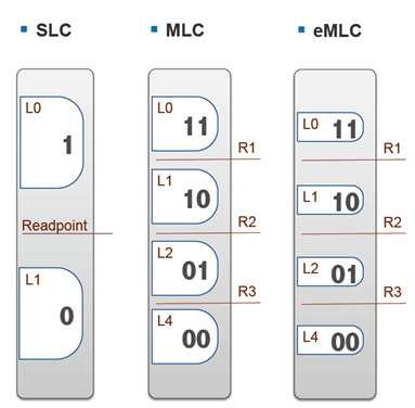
SLC, MLC & eMLCSee Intel 20nm process  technology from March 2012 Micron/ Intel 20-nm 64G MLC NAND Flash Memory Reverse Engineered

3D is likely to be a strong contender for scaling leading edge NAND flash.

See Samsung Advances Memory Storage eMMC to 1x-nm Process regarding what 10 nm really is.

Ron
Insightful, timely, and accurate semiconductor consulting.Semiconductor information and news at - www.maltiel-consulting.com


Samsung hits triple-level-cell NAND flash milestone

Arabinda Das, 5/1/2013 1:32 PM EDT

http://www.eetimes.com/design/memory-design/4413213/Samsung-hits-triple-level-cell-NAND-flash-milestone?pageNumber=0&goback=%2Egde_1803012_member_237577215


Samsung announced recently that it started production of advanced NAND flash devices with 128Gbit, triple-level cell (TLC) NAND memory using 10-nm class process technology.

Similarly, Micron also announced in February that it would come to market with NAND flash devices with a memory capacity of 128 Gbit that also use TLC design. It was only last fall that Samsung introduced a 64 Gbit NAND flash using TLC and 21-nm process technology.

Clearly, the industry is moving toward TLC cell design even for demanding SSD applications. The concept of a multi-bit per cell technology was first introduced by Toshiba and for the last five years, all flash device makers have products using the 2-bit per cell design. (Download TechInsights' flash NAND technology roadmap here).

A multi-bit cell device has a high density and a low cost per bit, but usually has a reduced endurance. In a conventional single bit flash device the number of electrons placed on the floating gate affects the threshold voltage (Vt) of the cell. This effect is used to set the state of the cell to either high or low.

In a multi-bit cell the threshold is set to several different values. The difference in voltage between these levels is small, which puts an additional constraint of placing the charge precisely on the floating gate and of sensing it correctly. In a 2 bit per cell memory, the cell is put in four states. In a 3-bit per cell there are eight states (states = 2n), which imposes a colossal task for flash device manufactures to have a tight cell threshold voltage distribution and a precise sensing of cell data.

According to several papers, the number of electrons stored on a floating gate for the 30-nm node class is slightly less than 100. So, in a 21-nm node with the TLC design, the circuitry for placing and sensing charge on the floating gate is dealing with only a few tens of electrons in each state.

Therefore, Samsung’s 21-nm, 64 Gbit TLC NAND flash can be considered an industry milestone. It is the first commercial SSD product using the TLC design in 21 nm node. TechInsights has done a structural analysis of the 21-nm, 64 Gbit TLC NAND flash and is also following up with a waveform analysis.

The K9CFGY8U5A-CCK0  21-nm flash memory  is one of the industry’s leading flash memory devices, packing 64G bits into a single 102.87 mm2 die, using conventional floating-gate flash memory technology. This NAND flash was found in Samsung’s latest SSD drive, the SSD840 (256GB). The basic teardown of the SSD drive is shown in figure 1.

Samsung's 21 nm NAND flash device is fabricated using a triple metal, double poly, 21-nm CMOS process. The single transistor flash cell measures approximately 42 nm by 46 nm for a physical cell area of 0.0019 µm2.  Its  competitors  in  process technology include  a 19-nm, 32-Gbit  MLC  NAND  flash from Toshiba and   a  20 nm 32 Gbit MLC NAND Flash from Intel-Micron.

Floating gate technology.
All NAND flash memories continue to evolve the floating gate technology. But the basic cell structure has remained unchanged throughout several process generations. The self-aligned floating gate poly (SAP) process is still used by the three major manufactures.

Intra-gate poly to poly contacts are adopted by all manufacturers. In fact, two of the major manufacturers are still using the control gate (CG) and inter-poly dielectric (IPD) wrap around the floating gate (FG) configuration. Managing to keep most of the processes steps the same as the previous node is a great advantage for manufacturing because all the accumulated experience in process development is utilized to produce the new generation of devices. And yet every new node is a technological feat.

With every new technology node, the memory density (Mbits/mm2) increases and the process technology becomes more complex because all features on the die shrink but do not shrink proportionately with the same ratio.

Figure 2, shows a compound picture where the top image is the SEM cross-section along the Bitline direction of Samsung 21-nm TLC NAND flash and the bottom image is the corresponding topographical image at poly Wordline level. Figure 2 shows that the NAND string is consisting of 64 active Wordlines, two dummy Wordlines two select transistors at both end of the Wordlines and two contacts (Sourceline and Bitline).


Figure 2: Correlating SEM cross-section in Bitline direction with topographical image at poly-Wordline level. The topographical image shows the staggered Bitline contact layout.

The ratio of the length of the active Wordlines to the NAND string length is the overhead factor. Table 1 recapitulates some of the important features of last three Samsung NAND flash devices. This table puts in evidence the fact that the active cells are shrinking more than the string-select and ground select transistors and as a consequence the NAND string overhead has been increasing for the last three generations. As the active cells shrink the close distance between adjacent floating gates leads to parasitic capacitance which may  result in a Vt shift. Samsung has done a major process change in 21-nm NAND flash devices to counter the parasitic capacitance issue as elaborated in Figure 3.


Table 1: Compiling some of the NAND cell features of last three Samsung NAND flashdevices. TLC designs make a huge impact on the memory density. As the technology scales down, the overhead seems to increase.Figure 1: Basic teardown, from SSD 840 drive to single NAND flash die.

Tungsten metal gate.
This 21-nm NAND flash has abandoned the silicide process and opted for tungsten metal gate. This transition is not new; it has already been done in many DRAM products. However, depositing tungsten on poly is not a straightforward process; several interface treatments have to be done, which are described in the report.

Tungsten metal gates leads to controllable air gaps, which mitigate the parasitic capacitance. Other challenges including choosing a suitable inter-poly-dielectric (IPD) layer. The IPD thickness affects program/erase speed and magnitude of read current and the quality of the dielectric layers has a direct impact on the endurance of the flash device. 

A thinner of IPD layer will increase the capacitive coupling between the control gate (CG) and the floating gate (FG) and generate a higher read current and a faster program erase mechanism but can also compromise the retention capability. So a tradeoff has to be made.

The IPD layer composition in 21-nm NAND flash is still the same as the previous generation but the individual layer thicknesses are modified. Also, in the Wordline direction, the aspect ratio for poly 2 gap-fill is greater than five. Here, too, Samsung has come up with new process techniques. Samsung’s 21-nm 64 Gbit TLC NAND flash technology has a process flow similar to its previous generation but with an enhanced process capability. It remains to be seen if the next generation 10-nm class 128-Gbits TLC NAND flash will manage to prolong the existing process flow or will take the next big step of fabricating 3-D NAND stacks.

Interested in NAND flash technology? You can check out TechInsights' technology roadmap for NAND flash here.

Arabinda Das is a senior process analyst at TechInsights.

Monday, March 4, 2013

Storage Memory Tipping Point

The storage tipping point is upon us
Ambuj Goyal 2/27/2013 2:01 AM EST
www.eetimes.com/electronics-blogs/other/4407874/storage-tipping-point-upon-us

Keeping pace with the onslaught of Big Data requires a revolutionary approach to storage. It’s well known that the performance of computing has advanced at a much faster rate than the systems that store and retrieve the information they generate.


For many, this game of catch-up has existed since the first digital storage systems were introduced more than 50 years ago. At the time, the concern was no longer about the performance of computing, but about creating a digital storage system that could keep up with it.

Thus began the subsequent watershed moves from paper punch cards to magnetic tape and then hard disk drives—moments that revolutionized computing and ultimately the world in which we live.

Today we find ourselves at another critical technological juncture that once again is demanding a revolutionary approach to storage—an approach that will help it keep pace with not only computing, but with the information onslaught of Big Data.
To understand where the storage industry is headed, one need only look to the reason that computing has historically outpaced it. Unlike the storage industry, computing has continually leveraged and advanced semiconductor trends while storage systems have remained mechanical, with motorized wheels of tape or spinning disks. In fact, computing shifted from mechanical devices more than a hundred years ago, while digital storage, for the most part, remains tethered to technologies born out of the 1950’s.

Not any longer. We are at the tipping point of a new era of computer storage that will witness entire systems based on flash semiconductor memory to handle fast moving, operational data in real-time. Though flash has been utilized in a variety of capacities over the past 30 years and in hybrid storage systems over the past several years, complete flash systems will dominate the landscape in the coming months and years.

All-flash systems will not only provide exponential performance gains over mechanical and hybrid systems, they will help organizations dramatically lower data center energy consumption rates due to their inherent low power-consuming memory and lack of moving parts—no small feat. According to a 2011 study by Stanford University, data centers account for 2 percent of all the electricity consumed in the U.S.

Improved performance, reliability, and durability

To be sure, such systems will be the storage platform of choice to handle ever-growing and increasingly critical workloads such as credit card processing, stock exchange transactions, manufacturing and order processing systems. Even app stores on the web are starting to use flash-only storage.

Such attributes as improved performance, reliability, and durability make flash systems desirable today, but virtually mandatory for the future. That’s because the tsunami of Big Data shows no sign of receding. Researchers predict that the digital universe—all the digital information created around the world—will hit 8 zettabytes by 2015. That’s about all the data found in the U.S. Library of Congress times 800 million.

Today we find ourselves at a tipping point of computer storage, once again, where the challenges of computing are no longer at issue but, rather the storing and retrieving of the information they generate and share.

Through our acquisition of Texas Memory Systems last fall, we have systems that can store almost 24 terabytes of storage in a unit the size of a pizza box, and that provide access to data 100 times faster than mechanical storage. If we were to stack 42 such pizza boxes in a rack, it would provide 1 petabyte of storage, which is more storage than any single operational application requires.
The industry is moving rapidly in the direction of all-flash storage for operational information. Such systems will not only help organizations respond to, and exploit the challenges of Big Data today and tomorrow, but once again will change the future of computing and the possibly the world along with it.
Ambuj Goyal is general manager of IBM System Storage & Networking.

Wednesday, January 30, 2013

Where is DRAM Innovation?


The article, Hynix 30 nm DRAM layout, process integration adapt to change ,  discusses advances in DRAM memory at Hynix. DRAM memory has not been able to shrink the memory cell as quickly as flash memory. Leading edge flash memory products with dimensions around 20nm or less are being introduced to production, while DRAM memory is still above 30nm (see figure 4 in the article below).


While flash memory has a key advantage of keeping the information even without power, there is still a place for DRAM memory. Many of the process technology advances are being implemented at a slower rate in DRAM production. However major memory cell and circuit improvements are not being pursued. For example, storing multiple bites in one physical flash memory cell has been done for several years. There are 3-bit-per-cell (TLC) NAND and 2-bit-per-cell (MLC) flash available in the market, but there is no DRAM product with multiple bits in the same cell.

Ron

Insightful, timely, and accurate semiconductor consulting.
Semiconductor information and news at - http://www.maltiel-consulting.com/


Tuesday, January 22, 2013

MLC Flash Memory New Future

A new development by Macronix has the potential of extending flash NAND memory technology for several additional generations.


In 2012 IEDM conference Macronix engineers presented a paper on radically improving flash memory program /erase cycling endurance to more than 100 million cycles by localized heat treatment .  Currently, most advance flash NAND products are limited to less than 100,000 cycles. The larger memory devices, called MLC flash, can store 2 or 3 bits in each memory cell. However, their cycling endurance is limited to less than 10,000 cycles. The new heating method will increase the cycling endurance of MLC flash. An improved cycling endurance would enable development of higher density MLC flash cells with larger numbers of bits per cell.

Macronix's new heat treatment that heals the memory cell can impact other layers in the memory cell. For example, it can change electromigration properties of metal lines nearby. It can also produce mechanical stress around the heat spots. The impact of the heat treatment has to be optimized, since the potential of creating larger flash memory looks promising. Already Macronix will present a flash memory chip with 6 bits per cell at the 2013 ISSCC.


Ron

Insightful, timely, and accurate semiconductor consulting.
Semiconductor information and news at - http://www.maltiel-consulting.com/


Monday, January 7, 2013

3D Flash Memory Marching Forward

3-D Flash starts to appear in the market. Hynix version is based on VSAT technology.


See more about VSAT at http://www.maltiel-consulting.com/3D_Charge_Trapping-CT_NAND_Flash.pdf .


The dramatic iincrease in flash memory cycling endurance (mentioned in IEDM 2012) is likely to extend the life of the basic flash NAND technology.


Ron
Insightful, timely, and accurate semiconductor consulting.
Semiconductor information and news at - http://www.maltiel-consulting.com/


Hynix to start sampling 3D flash memory chips

04 Jan 2013

South Korean memory semiconductor supplier SK Hynix said earlier this week that it would begin mass production and sampling of 3D flash memory chips that utilises vertical-stacked-array-transistor (VSAT) technology, according to a report by the Korea Times.

Flash chip, which is a type of non-volatile memory that can be erased and reprogrammed, is ideal for data-intensive devices that constantly connect to the Internet. It has a simple cell structure that allows for higher memory capacity, density and durability.
"As far as I know, all major semiconductor companies are investing more in the development of 3D flash memory chips. SK Hynix is trying hard to mass produce them as early as possible," said CTO Park Sung-wook. Samsung Electronics is reportedly planning to produce 3D flash memory chips in its plant in Xi'an, China upon completion of the facility.

Wednesday, March 28, 2012

Micron/ Intel 20-nm 64G MLC NAND Flash Memory Reverse Engineered

Intel and Micron’s joint venture for process development, IM Flash Technologies (IMFT), has successfully developed and manufactured high density multi-level NAND flash memories with a 20-nm design rule for the first time. IMFT also revealed a fully planar floating gate cell design.


IMFT has introduced a cell planarization integrating with high-k/metal gate (HKMG) stack.For a new cell structure, oxide-nitride-oxide (ONO) inter-gate dielectric layer is replaced by a stack of high-k dielectrics to restore the FG to CG coupling ratio. Thinner polysilicon floating gate technology is likely adopted to lower the cell-to-cell interference.


An air gap isolation process is adopted to reduce capacitance coupling between cells (more below).


Ron Maltiel


Delving deep into Micron and Intel’s 20-nm 64-Gbit MLC NAND flash memory

http://www.eetimes.com/electronics-blogs/other/4369862/Delving-deep-into-Micron-and-Intel-s-20-nm-64-Gbit-MLC-NAND-flash-memory?pageNumber=0
Young-Min Kwon,                                                                      3/26/2012 7:38 PM EDT

UBM TechInsights recently analyzed IMFT's 20-nm, 64-Gbit MLC NAND to get a better understanding of the advanced process technologies and innovative cell architecture. The success of NAND flash memory in the semiconductor market is mainly driven by continuous and tremendous growth in the mobile phone and tablet PC markets, and the growth of adoption of high performance solid state drives (SSDs) as a replacement for hard drives in computers. As Intel and Micron jointly announced last year, a NAND flash product with a terabit capacity, comprising a simple stack of several dice, can be realized with the advent of 20-nm manufacturing technology in conjunction with a break-through concept in cell architecture.

During the past years, NAND flash has enjoyed the highest density among the commercial memories due to its excellent physical scalability and multi-level cell (MLC) approach with two or three bits per cell. However, the recent demand spike for NAND flash memories in portable electronics has resulted in a much drastic scaling down of the device structure of NAND to obtain higher density, faster speed and lower bit cost devices. The aggressive scaling of a cell size in NAND flash memory is expected to face severe barriers in sub-20-nm floating gate-based flash cell with conventional architecture.

In response to the challenges mentioned, Intel and Micron’s joint venture for process development, IM Flash Technologies (IMFT), aggressively pursued a NAND cell shrink, and, as a result, has successfully developed and manufactured high density multi-level NAND flash memories with a 20-nm design rule for the first time. IMFT also revealed an innovative memory structure with the introduction of a fully planar floating gate cell design. IMFT, often considered a leader in the NAND flash manufacturing process, has introduced a cell planarization integrating with high-k/metal gate (HKMG) stack that would considerably overcome many of the physical and electrical scaling challenges brought on by moving to the 20-nm node or further beyond.

UBM TechInsights recently analyzed IMFT's 20-nm 64Gbit MLC NAND to get a better understanding of the advanced process technologies and innovative cell architecture.

By introducing the 20-nm process technology in the production of their 64-Gbit MLCNAND flash memory, IMFT establishes itself as the leader in new process node implementation. Measuring in with a die size of just 117 mm2, this NAND device features an area size that is approximately a 30 percent reduction over the IMFT’s existing 25-nm 64-Gbit NAND flash. IMFT’s 64-Gbit NAND flash is fabricated in a single poly, metal gate and triple metal levels and is distributed in a 48-pin lead-free TSOP package. The 64-Gbit of single flash memory die is divided into four banks with one-sided bond pad arrangement and memory area efficiency is 52% which is comparable to previous 25-nm 64-Gbit NAND device having the die size of 162 mm2.


In a conventional NAND floating gate cell, the control gate (CG) and inter-poly dielectric wrap around the floating gate (FG) and coupling factor greatly relies on the floating gate sidewalls as shown in the figure below.


Conventional floating gate NAND (IMFT’s 25 nm NAND flash)


Delving deeper

For the 20-nm and below technology node, the cell spacing is already too narrow to allow a control gate plug between the floating gates. As a result, the NAND flash memory will have to adopt a planar cell configuration by eliminating the control gate-floating gate wraparound.

Charge trapping-based flash (CTF) memory had been considered as an alternative, with CTF having a planar cell structure, but unfortunately we have yet to see a successful debut in NAND production quite yet. With all these factors at play, metal as control gate in combination with a stack of high-k inter-gate dielectrics (IGD) above thinner floating gate would be the potential solution to continue the scaling of NAND flash beyond the 20-nm node with existing floating gate-based NAND flash technology.


Planar floating gate NAND (IMFT’s 20-nm NAND flash)

Key technologies in the process and new flash cell structure

IMFT's 20-nm technology with a fully planar cell structure and key process advances have overcome several critical problems of conventional floating gate cell architectures in such a small flash device:

• Control gate (CG) poly-Si filling to narrower space between adjacent floating gates

• Cell-to-cell interference

• Scaling limitation of inter-poly dielectric (IPD) and smaller CG to FG coupling ratio.

In order to manufacture a 20-nm NAND cell, advanced cell pitch reduction techniques (such as double patterning technology) are used for critical lithographic steps. To pattern below the 20-nm design rule, quad patterning technology will also have to be implemented to overcome the limitation of 193 nm ArF immersion double patterning. This, however, could be still a ways away as the extreme ultraviolet lithography (EUV) tool required to address this patterning issue is still too expensive for flash memory production. For this NAND component, a single flash cell measures around 40-nm in both the wordline and the bitline direction yielding a physical cell area of 0.0017 µm2. That makes this cell most likely the smallest cell in NAND production. A planar floating gate structure has been implemented in this NAND device, in conjunction with thin polysilicon floating gate, a stack of high-k inter-gate dielectrics (IGD), and metal control gate.

For a new cell structure, oxide-nitride-oxide (ONO) inter-gate dielectric layer is replaced by a stack of high-k dielectrics to restore the FG to CG coupling ratio which should be reduced in planar cell structure. Thinner polysilicon floating gate technology is likely adopted to lower the cell-to-cell interference. A metal gate-based wordline is defined by etching the multiple gate stacks using the hard mask layer. As the cell pitch is aggressively scaled, the increased capacitance coupling between cells is a severe issue, since increased cell-to-cell interference leads to cell performance degradation and reliability problem. In order to overcome these problems, an air gap isolation process is adopted for both cell gates and metal 1 bitlines. An air gap structure has been reported to act as a low dielectric constant gap filling materials. The bitline contacts are formed as a staggered layout to obtain better lithographic margin, and a NAND string has 68 wordlines.

New cell architecture combined with key integration technologies observed from IMFT’s 20-nm MLC NAND flash is very promising to further extend the life span of conventional floating gate flash memory with more aggressive cell scaling. However, with a further reduced geometry of floating gate, the electrons captured will be drastically decreased, which could result in the need to manage less than 20 electrons in 1x-nm MLC NAND flash. That’s why novel device concepts or alternative memory solutions, such as those found in IMFT’s latest NAND flash device, reveal a preparedness to replace NAND flash memory in near future since scaling demand and reliability challenges will be much higher in dominant mobile applications. For example, the CTF seen in this NAND coupled with 3-D configuration could be seen as a viable near-term alternative to current planar NAND flash technology while a large variety of new memory concepts are emerging and competing for the replacement of NAND flash memory. Floating gate NAND flash will eventually arrive at its scaling limit but it’s not quite hitting the wall just yet. It will be very interesting to see what changes IMFT, and other flash manufacturers, incorporate to overcome these scaling limitations in the future.