"Samsung's 21 nm NAND flash device is fabricated using a triple metal, double poly, 21-nm CMOS process. The single transistor flash cell measures approximately 42 nm by 46 nm for a physical cell area of 0.0019 µm2. Its competitors in process technology include a 19-nm, 32-Gbit MLC NAND flash from Toshiba and a 20 nm 32 Gbit MLC NAND Flash from Intel-Micron."
 See Intel 20nm process technology from March 2012 Micron/ Intel 20-nm 64G MLC NAND Flash Memory Reverse Engineered
3D is likely to be a strong contender for scaling leading edge NAND flash.
See Samsung Advances Memory Storage eMMC to 1x-nm Process regarding what 10 nm really is.
Ron
Insightful, timely, and accurate semiconductor consulting.Semiconductor information and news at - www.maltiel-consulting.com
Samsung hits triple-level-cell NAND flash milestone
http://www.eetimes.com/design/memory-design/4413213/Samsung-hits-triple-level-cell-NAND-flash-milestone?pageNumber=0&goback=%2Egde_1803012_member_237577215
Samsung announced recently that it started production of advanced NAND flash devices with 128Gbit, triple-level cell (TLC) NAND memory using 10-nm class process technology.
Similarly, Micron also announced in February that it would come to market with NAND flash devices with a memory capacity of 128 Gbit that also use TLC design. It was only last fall that Samsung introduced a 64 Gbit NAND flash using TLC and 21-nm process technology.
Clearly, the industry is moving toward TLC cell design even for demanding SSD applications. The concept of a multi-bit per cell technology was first introduced by Toshiba and for the last five years, all flash device makers have products using the 2-bit per cell design. (Download TechInsights' flash NAND technology roadmap here).
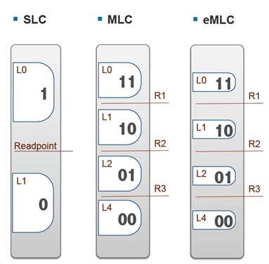
A multi-bit cell device has a high density and a low cost per bit, but usually has a reduced endurance. In a conventional single bit flash device the number of electrons placed on the floating gate affects the threshold voltage (Vt) of the cell. This effect is used to set the state of the cell to either high or low.
In a multi-bit cell the threshold is set to several different values. The difference in voltage between these levels is small, which puts an additional constraint of placing the charge precisely on the floating gate and of sensing it correctly. In a 2 bit per cell memory, the cell is put in four states. In a 3-bit per cell there are eight states (states = 2n), which imposes a colossal task for flash device manufactures to have a tight cell threshold voltage distribution and a precise sensing of cell data.
According to several papers, the number of electrons stored on a floating gate for the 30-nm node class is slightly less than 100. So, in a 21-nm node with the TLC design, the circuitry for placing and sensing charge on the floating gate is dealing with only a few tens of electrons in each state.
Therefore, Samsung’s 21-nm, 64 Gbit TLC NAND flash can be considered an industry milestone. It is the first commercial SSD product using the TLC design in 21 nm node. TechInsights has done a structural analysis of the 21-nm, 64 Gbit TLC NAND flash and is also following up with a waveform analysis.
The K9CFGY8U5A-CCK0 21-nm flash memory is one of the industry’s leading flash memory devices, packing 64G bits into a single 102.87 mm2 die, using conventional floating-gate flash memory technology. This NAND flash was found in Samsung’s latest SSD drive, the SSD840 (256GB). The basic teardown of the SSD drive is shown in figure 1.
Samsung's 21 nm NAND flash device is fabricated using a triple metal, double poly, 21-nm CMOS process. The single transistor flash cell measures approximately 42 nm by 46 nm for a physical cell area of 0.0019 µm2. Its competitors in process technology include a 19-nm, 32-Gbit MLC NAND flash from Toshiba and a 20 nm 32 Gbit MLC NAND Flash from Intel-Micron.

Floating gate technology.
All NAND flash memories continue to evolve the floating gate technology. But the basic cell structure has remained unchanged throughout several process generations. The self-aligned floating gate poly (SAP) process is still used by the three major manufactures.
Intra-gate poly to poly contacts are adopted by all manufacturers. In fact, two of the major manufacturers are still using the control gate (CG) and inter-poly dielectric (IPD) wrap around the floating gate (FG) configuration. Managing to keep most of the processes steps the same as the previous node is a great advantage for manufacturing because all the accumulated experience in process development is utilized to produce the new generation of devices. And yet every new node is a technological feat.
With every new technology node, the memory density (Mbits/mm2) increases and the process technology becomes more complex because all features on the die shrink but do not shrink proportionately with the same ratio.
Figure 2, shows a compound picture where the top image is the SEM cross-section along the Bitline direction of Samsung 21-nm TLC NAND flash and the bottom image is the corresponding topographical image at poly Wordline level. Figure 2 shows that the NAND string is consisting of 64 active Wordlines, two dummy Wordlines two select transistors at both end of the Wordlines and two contacts (Sourceline and Bitline).

Figure 2: Correlating SEM cross-section in Bitline direction with topographical image at poly-Wordline level. The topographical image shows the staggered Bitline contact layout.
The ratio of the length of the active Wordlines to the NAND string length is the overhead factor. Table 1 recapitulates some of the important features of last three Samsung NAND flash devices. This table puts in evidence the fact that the active cells are shrinking more than the string-select and ground select transistors and as a consequence the NAND string overhead has been increasing for the last three generations. As the active cells shrink the close distance between adjacent floating gates leads to parasitic capacitance which may result in a Vt shift. Samsung has done a major process change in 21-nm NAND flash devices to counter the parasitic capacitance issue as elaborated in Figure 3.

Table 1: Compiling some of the NAND cell features of last three Samsung NAND flashdevices. TLC designs make a huge impact on the memory density. As the technology scales down, the overhead seems to increase.Figure 1: Basic teardown, from SSD 840 drive to single NAND flash die.
Similarly, Micron also announced in February that it would come to market with NAND flash devices with a memory capacity of 128 Gbit that also use TLC design. It was only last fall that Samsung introduced a 64 Gbit NAND flash using TLC and 21-nm process technology.
Clearly, the industry is moving toward TLC cell design even for demanding SSD applications. The concept of a multi-bit per cell technology was first introduced by Toshiba and for the last five years, all flash device makers have products using the 2-bit per cell design. (Download TechInsights' flash NAND technology roadmap here).
A multi-bit cell device has a high density and a low cost per bit, but usually has a reduced endurance. In a conventional single bit flash device the number of electrons placed on the floating gate affects the threshold voltage (Vt) of the cell. This effect is used to set the state of the cell to either high or low.
In a multi-bit cell the threshold is set to several different values. The difference in voltage between these levels is small, which puts an additional constraint of placing the charge precisely on the floating gate and of sensing it correctly. In a 2 bit per cell memory, the cell is put in four states. In a 3-bit per cell there are eight states (states = 2n), which imposes a colossal task for flash device manufactures to have a tight cell threshold voltage distribution and a precise sensing of cell data.
According to several papers, the number of electrons stored on a floating gate for the 30-nm node class is slightly less than 100. So, in a 21-nm node with the TLC design, the circuitry for placing and sensing charge on the floating gate is dealing with only a few tens of electrons in each state.
Therefore, Samsung’s 21-nm, 64 Gbit TLC NAND flash can be considered an industry milestone. It is the first commercial SSD product using the TLC design in 21 nm node. TechInsights has done a structural analysis of the 21-nm, 64 Gbit TLC NAND flash and is also following up with a waveform analysis.
The K9CFGY8U5A-CCK0 21-nm flash memory is one of the industry’s leading flash memory devices, packing 64G bits into a single 102.87 mm2 die, using conventional floating-gate flash memory technology. This NAND flash was found in Samsung’s latest SSD drive, the SSD840 (256GB). The basic teardown of the SSD drive is shown in figure 1.
Samsung's 21 nm NAND flash device is fabricated using a triple metal, double poly, 21-nm CMOS process. The single transistor flash cell measures approximately 42 nm by 46 nm for a physical cell area of 0.0019 µm2. Its competitors in process technology include a 19-nm, 32-Gbit MLC NAND flash from Toshiba and a 20 nm 32 Gbit MLC NAND Flash from Intel-Micron.
Floating gate technology.
All NAND flash memories continue to evolve the floating gate technology. But the basic cell structure has remained unchanged throughout several process generations. The self-aligned floating gate poly (SAP) process is still used by the three major manufactures.
Intra-gate poly to poly contacts are adopted by all manufacturers. In fact, two of the major manufacturers are still using the control gate (CG) and inter-poly dielectric (IPD) wrap around the floating gate (FG) configuration. Managing to keep most of the processes steps the same as the previous node is a great advantage for manufacturing because all the accumulated experience in process development is utilized to produce the new generation of devices. And yet every new node is a technological feat.
With every new technology node, the memory density (Mbits/mm2) increases and the process technology becomes more complex because all features on the die shrink but do not shrink proportionately with the same ratio.
Figure 2, shows a compound picture where the top image is the SEM cross-section along the Bitline direction of Samsung 21-nm TLC NAND flash and the bottom image is the corresponding topographical image at poly Wordline level. Figure 2 shows that the NAND string is consisting of 64 active Wordlines, two dummy Wordlines two select transistors at both end of the Wordlines and two contacts (Sourceline and Bitline).
Figure 2: Correlating SEM cross-section in Bitline direction with topographical image at poly-Wordline level. The topographical image shows the staggered Bitline contact layout.
The ratio of the length of the active Wordlines to the NAND string length is the overhead factor. Table 1 recapitulates some of the important features of last three Samsung NAND flash devices. This table puts in evidence the fact that the active cells are shrinking more than the string-select and ground select transistors and as a consequence the NAND string overhead has been increasing for the last three generations. As the active cells shrink the close distance between adjacent floating gates leads to parasitic capacitance which may result in a Vt shift. Samsung has done a major process change in 21-nm NAND flash devices to counter the parasitic capacitance issue as elaborated in Figure 3.
Tungsten metal gate.
This 21-nm NAND flash has abandoned the silicide process and opted for tungsten metal gate. This transition is not new; it has already been done in many DRAM products. However, depositing tungsten on poly is not a straightforward process; several interface treatments have to be done, which are described in the report.
Tungsten metal gates leads to controllable air gaps, which mitigate the parasitic capacitance. Other challenges including choosing a suitable inter-poly-dielectric (IPD) layer. The IPD thickness affects program/erase speed and magnitude of read current and the quality of the dielectric layers has a direct impact on the endurance of the flash device.
A thinner of IPD layer will increase the capacitive coupling between the control gate (CG) and the floating gate (FG) and generate a higher read current and a faster program erase mechanism but can also compromise the retention capability. So a tradeoff has to be made.
The IPD layer composition in 21-nm NAND flash is still the same as the previous generation but the individual layer thicknesses are modified. Also, in the Wordline direction, the aspect ratio for poly 2 gap-fill is greater than five. Here, too, Samsung has come up with new process techniques. Samsung’s 21-nm 64 Gbit TLC NAND flash technology has a process flow similar to its previous generation but with an enhanced process capability. It remains to be seen if the next generation 10-nm class 128-Gbits TLC NAND flash will manage to prolong the existing process flow or will take the next big step of fabricating 3-D NAND stacks.
Interested in NAND flash technology? You can check out TechInsights' technology roadmap for NAND flash here.
Arabinda Das is a senior process analyst at TechInsights.
This 21-nm NAND flash has abandoned the silicide process and opted for tungsten metal gate. This transition is not new; it has already been done in many DRAM products. However, depositing tungsten on poly is not a straightforward process; several interface treatments have to be done, which are described in the report.
Tungsten metal gates leads to controllable air gaps, which mitigate the parasitic capacitance. Other challenges including choosing a suitable inter-poly-dielectric (IPD) layer. The IPD thickness affects program/erase speed and magnitude of read current and the quality of the dielectric layers has a direct impact on the endurance of the flash device.
A thinner of IPD layer will increase the capacitive coupling between the control gate (CG) and the floating gate (FG) and generate a higher read current and a faster program erase mechanism but can also compromise the retention capability. So a tradeoff has to be made.
The IPD layer composition in 21-nm NAND flash is still the same as the previous generation but the individual layer thicknesses are modified. Also, in the Wordline direction, the aspect ratio for poly 2 gap-fill is greater than five. Here, too, Samsung has come up with new process techniques. Samsung’s 21-nm 64 Gbit TLC NAND flash technology has a process flow similar to its previous generation but with an enhanced process capability. It remains to be seen if the next generation 10-nm class 128-Gbits TLC NAND flash will manage to prolong the existing process flow or will take the next big step of fabricating 3-D NAND stacks.
Interested in NAND flash technology? You can check out TechInsights' technology roadmap for NAND flash here.
Arabinda Das is a senior process analyst at TechInsights.


