Showing posts with label FG. Show all posts

Tuesday, July 23, 2013

SanDisk and 3D NAND


SanDisk is strongly pursuing 3D NAND  with Toshiba. 3D NAND is a very strong contender for future advances in NAND shrinking. See more below


Some background about 3D NAND and at
3D NAND flash is coming

 Ron
Insightful, timely, and accurate semiconductor consulting.
Semiconductor information and news at - http://www.maltiel-consulting.com/


SanDisk starts beating path to 3D NAND flash

Reckons product ready for market by 2015

Friday, May 3, 2013

Samsung NAND 1xnm Manufacturing TLC (Triple Level)

The article below discuss leading edge process and cell technology of 20 nm flash NAND cell.

"Samsung's 21 nm NAND flash device is fabricated using a triple metal, double poly, 21-nm CMOS process. The single transistor flash cell measures approximately 42 nm by 46 nm for a physical cell area of 0.0019 µm2.  Its  competitors  in  process technology include  a 19-nm, 32-Gbit  MLC  NAND  flash from Toshiba and   a  20 nm 32 Gbit MLC NAND Flash from Intel-Micron."

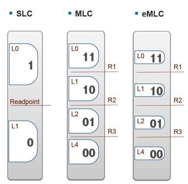
SLC, MLC & eMLCSee Intel 20nm process  technology from March 2012 Micron/ Intel 20-nm 64G MLC NAND Flash Memory Reverse Engineered

3D is likely to be a strong contender for scaling leading edge NAND flash.

See Samsung Advances Memory Storage eMMC to 1x-nm Process regarding what 10 nm really is.

Ron
Insightful, timely, and accurate semiconductor consulting.Semiconductor information and news at - www.maltiel-consulting.com


Samsung hits triple-level-cell NAND flash milestone

Arabinda Das, 5/1/2013 1:32 PM EDT

http://www.eetimes.com/design/memory-design/4413213/Samsung-hits-triple-level-cell-NAND-flash-milestone?pageNumber=0&goback=%2Egde_1803012_member_237577215


Samsung announced recently that it started production of advanced NAND flash devices with 128Gbit, triple-level cell (TLC) NAND memory using 10-nm class process technology.

Similarly, Micron also announced in February that it would come to market with NAND flash devices with a memory capacity of 128 Gbit that also use TLC design. It was only last fall that Samsung introduced a 64 Gbit NAND flash using TLC and 21-nm process technology.

Clearly, the industry is moving toward TLC cell design even for demanding SSD applications. The concept of a multi-bit per cell technology was first introduced by Toshiba and for the last five years, all flash device makers have products using the 2-bit per cell design. (Download TechInsights' flash NAND technology roadmap here).

A multi-bit cell device has a high density and a low cost per bit, but usually has a reduced endurance. In a conventional single bit flash device the number of electrons placed on the floating gate affects the threshold voltage (Vt) of the cell. This effect is used to set the state of the cell to either high or low.

In a multi-bit cell the threshold is set to several different values. The difference in voltage between these levels is small, which puts an additional constraint of placing the charge precisely on the floating gate and of sensing it correctly. In a 2 bit per cell memory, the cell is put in four states. In a 3-bit per cell there are eight states (states = 2n), which imposes a colossal task for flash device manufactures to have a tight cell threshold voltage distribution and a precise sensing of cell data.

According to several papers, the number of electrons stored on a floating gate for the 30-nm node class is slightly less than 100. So, in a 21-nm node with the TLC design, the circuitry for placing and sensing charge on the floating gate is dealing with only a few tens of electrons in each state.

Therefore, Samsung’s 21-nm, 64 Gbit TLC NAND flash can be considered an industry milestone. It is the first commercial SSD product using the TLC design in 21 nm node. TechInsights has done a structural analysis of the 21-nm, 64 Gbit TLC NAND flash and is also following up with a waveform analysis.

The K9CFGY8U5A-CCK0  21-nm flash memory  is one of the industry’s leading flash memory devices, packing 64G bits into a single 102.87 mm2 die, using conventional floating-gate flash memory technology. This NAND flash was found in Samsung’s latest SSD drive, the SSD840 (256GB). The basic teardown of the SSD drive is shown in figure 1.

Samsung's 21 nm NAND flash device is fabricated using a triple metal, double poly, 21-nm CMOS process. The single transistor flash cell measures approximately 42 nm by 46 nm for a physical cell area of 0.0019 µm2.  Its  competitors  in  process technology include  a 19-nm, 32-Gbit  MLC  NAND  flash from Toshiba and   a  20 nm 32 Gbit MLC NAND Flash from Intel-Micron.

Floating gate technology.
All NAND flash memories continue to evolve the floating gate technology. But the basic cell structure has remained unchanged throughout several process generations. The self-aligned floating gate poly (SAP) process is still used by the three major manufactures.

Intra-gate poly to poly contacts are adopted by all manufacturers. In fact, two of the major manufacturers are still using the control gate (CG) and inter-poly dielectric (IPD) wrap around the floating gate (FG) configuration. Managing to keep most of the processes steps the same as the previous node is a great advantage for manufacturing because all the accumulated experience in process development is utilized to produce the new generation of devices. And yet every new node is a technological feat.

With every new technology node, the memory density (Mbits/mm2) increases and the process technology becomes more complex because all features on the die shrink but do not shrink proportionately with the same ratio.

Figure 2, shows a compound picture where the top image is the SEM cross-section along the Bitline direction of Samsung 21-nm TLC NAND flash and the bottom image is the corresponding topographical image at poly Wordline level. Figure 2 shows that the NAND string is consisting of 64 active Wordlines, two dummy Wordlines two select transistors at both end of the Wordlines and two contacts (Sourceline and Bitline).


Figure 2: Correlating SEM cross-section in Bitline direction with topographical image at poly-Wordline level. The topographical image shows the staggered Bitline contact layout.

The ratio of the length of the active Wordlines to the NAND string length is the overhead factor. Table 1 recapitulates some of the important features of last three Samsung NAND flash devices. This table puts in evidence the fact that the active cells are shrinking more than the string-select and ground select transistors and as a consequence the NAND string overhead has been increasing for the last three generations. As the active cells shrink the close distance between adjacent floating gates leads to parasitic capacitance which may  result in a Vt shift. Samsung has done a major process change in 21-nm NAND flash devices to counter the parasitic capacitance issue as elaborated in Figure 3.


Table 1: Compiling some of the NAND cell features of last three Samsung NAND flashdevices. TLC designs make a huge impact on the memory density. As the technology scales down, the overhead seems to increase.Figure 1: Basic teardown, from SSD 840 drive to single NAND flash die.

Tungsten metal gate.
This 21-nm NAND flash has abandoned the silicide process and opted for tungsten metal gate. This transition is not new; it has already been done in many DRAM products. However, depositing tungsten on poly is not a straightforward process; several interface treatments have to be done, which are described in the report.

Tungsten metal gates leads to controllable air gaps, which mitigate the parasitic capacitance. Other challenges including choosing a suitable inter-poly-dielectric (IPD) layer. The IPD thickness affects program/erase speed and magnitude of read current and the quality of the dielectric layers has a direct impact on the endurance of the flash device. 

A thinner of IPD layer will increase the capacitive coupling between the control gate (CG) and the floating gate (FG) and generate a higher read current and a faster program erase mechanism but can also compromise the retention capability. So a tradeoff has to be made.

The IPD layer composition in 21-nm NAND flash is still the same as the previous generation but the individual layer thicknesses are modified. Also, in the Wordline direction, the aspect ratio for poly 2 gap-fill is greater than five. Here, too, Samsung has come up with new process techniques. Samsung’s 21-nm 64 Gbit TLC NAND flash technology has a process flow similar to its previous generation but with an enhanced process capability. It remains to be seen if the next generation 10-nm class 128-Gbits TLC NAND flash will manage to prolong the existing process flow or will take the next big step of fabricating 3-D NAND stacks.

Interested in NAND flash technology? You can check out TechInsights' technology roadmap for NAND flash here.

Arabinda Das is a senior process analyst at TechInsights.

Wednesday, January 30, 2013

Where is DRAM Innovation?


The article, Hynix 30 nm DRAM layout, process integration adapt to change ,  discusses advances in DRAM memory at Hynix. DRAM memory has not been able to shrink the memory cell as quickly as flash memory. Leading edge flash memory products with dimensions around 20nm or less are being introduced to production, while DRAM memory is still above 30nm (see figure 4 in the article below).


While flash memory has a key advantage of keeping the information even without power, there is still a place for DRAM memory. Many of the process technology advances are being implemented at a slower rate in DRAM production. However major memory cell and circuit improvements are not being pursued. For example, storing multiple bites in one physical flash memory cell has been done for several years. There are 3-bit-per-cell (TLC) NAND and 2-bit-per-cell (MLC) flash available in the market, but there is no DRAM product with multiple bits in the same cell.

Ron

Insightful, timely, and accurate semiconductor consulting.
Semiconductor information and news at - http://www.maltiel-consulting.com/


Tuesday, January 22, 2013

MLC Flash Memory New Future

A new development by Macronix has the potential of extending flash NAND memory technology for several additional generations.


In 2012 IEDM conference Macronix engineers presented a paper on radically improving flash memory program /erase cycling endurance to more than 100 million cycles by localized heat treatment .  Currently, most advance flash NAND products are limited to less than 100,000 cycles. The larger memory devices, called MLC flash, can store 2 or 3 bits in each memory cell. However, their cycling endurance is limited to less than 10,000 cycles. The new heating method will increase the cycling endurance of MLC flash. An improved cycling endurance would enable development of higher density MLC flash cells with larger numbers of bits per cell.

Macronix's new heat treatment that heals the memory cell can impact other layers in the memory cell. For example, it can change electromigration properties of metal lines nearby. It can also produce mechanical stress around the heat spots. The impact of the heat treatment has to be optimized, since the potential of creating larger flash memory looks promising. Already Macronix will present a flash memory chip with 6 bits per cell at the 2013 ISSCC.


Ron

Insightful, timely, and accurate semiconductor consulting.
Semiconductor information and news at - http://www.maltiel-consulting.com/


Monday, January 7, 2013

3D Flash Memory Marching Forward

3-D Flash starts to appear in the market. Hynix version is based on VSAT technology.


See more about VSAT at http://www.maltiel-consulting.com/3D_Charge_Trapping-CT_NAND_Flash.pdf .


The dramatic iincrease in flash memory cycling endurance (mentioned in IEDM 2012) is likely to extend the life of the basic flash NAND technology.


Ron
Insightful, timely, and accurate semiconductor consulting.
Semiconductor information and news at - http://www.maltiel-consulting.com/


Hynix to start sampling 3D flash memory chips

04 Jan 2013

South Korean memory semiconductor supplier SK Hynix said earlier this week that it would begin mass production and sampling of 3D flash memory chips that utilises vertical-stacked-array-transistor (VSAT) technology, according to a report by the Korea Times.

Flash chip, which is a type of non-volatile memory that can be erased and reprogrammed, is ideal for data-intensive devices that constantly connect to the Internet. It has a simple cell structure that allows for higher memory capacity, density and durability.
"As far as I know, all major semiconductor companies are investing more in the development of 3D flash memory chips. SK Hynix is trying hard to mass produce them as early as possible," said CTO Park Sung-wook. Samsung Electronics is reportedly planning to produce 3D flash memory chips in its plant in Xi'an, China upon completion of the facility.

Monday, December 3, 2012

3D Flash NAND Devices and Process

The article below discusses developments in 3D Flash NAND. Toshiba and Macronix have different approaches. See more details about Toshiba Next NAND- 3D with 15 Layers.


Applied material discusses processing issues and new equipment to address them.

"According to Applied Materials, building 3D NAND structures in like trying to dig a one-kilometer-deep, three-kilometer-long trench with walls exactly three meters apart, through interleaved rock strata."

Ron Maltiel
www.maltiel-consulting.com


3D NAND flash is coming

http://www.edn.com/electronics-blogs/practical-chip-design/4401542/3D-NAND-flash-is-coming

Brian Bailey - November 15, 2012

Flash memory has very quickly risen from being an obscure memory type to perhaps becoming the dominant memory type for many devices, including music players, cell phones, tablets and now increasingly servers and mainstream PCs. But flash memory does not scale quite as well as the more traditional DRAM that it is replacing. It is thought that DRAM can scale down to 1nm whereas we are already hitting some problems with the scaling of the floating gate in NAND flash. It is not thought that planar NAND can go below 10nm which is only a couple of processes steps away from where we are today.


There are several other types of memory being developed, including spin-torque MRAM and Resistive RAM (ReRAM) that may replace both RAM and flash in the future. Another exciting direction is 3D NAND structures. In some respects this is similar to FinFET development for traditional transistors that are finding their way into 20nm and 14nm processes.


Toshiba is one company pushing 3D NAND processes with its p-BiCS (pipe-shaped Bit Cost Scalable) technology. The thought is that rather than lay the cells flat on the surface, higher densities can be achieved by stacking them on top of each other. This is shown diagrammatically in the figure below. As you can see this is not the same as 3D ICs where multiple substrates are layered on top of each other and connected using through silicon vias (TSV), this is building cells on top of each other to create U shaped bit lines. They currently have 16 layers devices where the hole size is 50nm and Toshiba says that the process becomes cheaper than the traditional NAND processes when more than 15 layers are created. Samples are expected next year and volume shipments by 2015...
  Additional details

Tuesday, October 16, 2012

Toshiba Next NAND- 3D with 15 Layers


The winner for the next flash memory approach is still not clear. A strong candidate is stacking memory NAND dies one on top of another. The dies are connected using Through Silicon Vias (TSV). Toshiba has a different approach to 3D " not stacking NAND chips one atop the other but rather stacking layers of NAND in a single chip" See more details below.

The key concern for next NAND generations is the 5 years lead time to build a new $5 billion fab, which could be designed for the wrong process technology.

It does not help that "the number of electrons in a gate decreases as the process geometry size is reduced....below 10nm the number of critical electrons in a gate can be as few as 10 – and that losing 10 electrons could seriously affect the gate's functioning. He says there are a variety of issues with such very small cells, such as bit-line loading, interference and leakage, leading to signal retention and reliability issues, for which, currently, there are no solutions.


These problems may make 10nm NAND technology impractical and sub-10nm impossible. Park suggests that 3D stacking, putting dies on on top of another, could be away out of this trap. He charts various approaches and identifies issues with each one, mentioning yield and retention as overall issues" (see more at Flashboys: HEELLLP, we're trapped in a process size shrink crunch)

Ron
www.maltiel-consulting.com


The 3D die stack tack: Toshiba builds towering column of flash


Resistance is futile
By Chris Mellor, 15th October 2012 09:28 GMT


Toshiba is building high rise flash and ReRAM chips, with prototypes coming next year and volume shipping in 2015.

The idea of high-rise or 3D chips is that we can sidestep limitations on increasing the storage density of flash or memory chips by stacking them one on top of the other, increasing the storage density on a Mbits/in 2 basis by building upwards, in the same way as high-rise housing increases the number of people living in the ground footprint of a block of flats.

Hot on the heels of our story about the NAND scaling trap [1], with 3D NAND and ReRAM suggested as two of the potential escape routes, we learn from Nikkei Electronics [2] that Toshiba is building 3D dies using a type of NAND, its p-BiCS (pipe-shaped Bit Cost Scalable) [3] technology, and also a coming replacement technology for NAND, ReRAM (Resistive RAM) which combines attributes of RAM and NAND to provide byte addressability, DRAM-class speed and NAND non-volatility.

As the slide below shows, 3D flash involves layers of NAND dies with communicating holes - TSVs or Through Silicon Vias - linking them to a stack controller at the base of the stack. It is not stacking NAND chips one atop the other but rather stacking layers of NAND in a single chip.


Toshiba p-BiCS technology [4]

Toshiba's p-BiCS NAND has a 50nm-size hole and 16 layers. Toshiba's chief engineer, Masaki Momodomi, at its Semiconductor & Storage Products Co., says that p-BiCS becomes cheaper than ordinary NAND when more than 15 layers are used, presumably comparing similar capacity levels. The company aims to deliver 128Gbit and 256Gbit prototype samples next year, engineering samples in 2014, with volume shipments in 2015; we are more than two years away from seeing product hit the streets.

The ReRAM [5] technology has a similar timescale though at lower capacities. It has much faster write times than NAND and Toshiba sees it fulfilling a different role from p-BiCS, being used closer to CPUs than p-BiCS, with STT-RAM being used for cache memories in, for example, SSDs. This is a similar hierarchy to the one proposed by Hynix in our NAND Scaling Trap story today. Jim Handy of Objective Analysis said; "It makes sense that ReRAM … would be used in performance applications, though. They are far faster at writes than NAND is, they are random access devices which NAND is not, and they don't need ECC. All this lends itself to faster performance."

Toshiba's ReRAM technology will appear in the same sequence of prototype samples, engineering samples and volume production as p-BiCS with the same general timing. A picture of a 64Gbit ReRAM device was shown at the Toshiba briefing attended by Nikkei Electronic but Toshiba intends to deliver generally equivalent p-BiCS and ReRAM capacities.

It is set of reducing the size of its current 1Xnm (19nm) NAND cells, and will target 1Ynm (18-14nm we understand) products this year and 1Znm (10-13nm) products next year.

Handy said: "All those new technologies (MRAM, ReRAM, FRAM...) perform better than NAND (BiCS is a kind of NAND) but are more costly. In memory cost is everything so these alternatives don't do well. The promise of these technologies is that they will move right past NAND's scaling limit. If they do that they will eventually become cheaper than NAND, but not until NAND has stopped scaling for 2 process generations.

"Toshiba talks about 1y and 1z, their processes after 19nm. I suspect that NAND will stop scaling at around 10nm, but BiCS will cause NAND pricing to continue to decline after that. Of course, those geniuses who have been coaxing NAND as far as 19nm could very well keep pulling rabbits out of their hats and push it well beyond 10nm - time will tell."

Will we see continued NAND process size decreases or 3D as the chosen way to get more capacity from a NAND die's footprint? Handy said: "The most recent ITRS [International Technology Roadmap for Semiconductors] [6] roadmap plots out two different directions for NAND - vertical (BiCS) and conventional. The industry really doesn't know where it's going to go, but it has plans in place for either eventuality."

Wednesday, March 28, 2012

Micron/ Intel 20-nm 64G MLC NAND Flash Memory Reverse Engineered

Intel and Micron’s joint venture for process development, IM Flash Technologies (IMFT), has successfully developed and manufactured high density multi-level NAND flash memories with a 20-nm design rule for the first time. IMFT also revealed a fully planar floating gate cell design.


IMFT has introduced a cell planarization integrating with high-k/metal gate (HKMG) stack.For a new cell structure, oxide-nitride-oxide (ONO) inter-gate dielectric layer is replaced by a stack of high-k dielectrics to restore the FG to CG coupling ratio. Thinner polysilicon floating gate technology is likely adopted to lower the cell-to-cell interference.


An air gap isolation process is adopted to reduce capacitance coupling between cells (more below).


Ron Maltiel


Delving deep into Micron and Intel’s 20-nm 64-Gbit MLC NAND flash memory

http://www.eetimes.com/electronics-blogs/other/4369862/Delving-deep-into-Micron-and-Intel-s-20-nm-64-Gbit-MLC-NAND-flash-memory?pageNumber=0
Young-Min Kwon,                                                                      3/26/2012 7:38 PM EDT

UBM TechInsights recently analyzed IMFT's 20-nm, 64-Gbit MLC NAND to get a better understanding of the advanced process technologies and innovative cell architecture. The success of NAND flash memory in the semiconductor market is mainly driven by continuous and tremendous growth in the mobile phone and tablet PC markets, and the growth of adoption of high performance solid state drives (SSDs) as a replacement for hard drives in computers. As Intel and Micron jointly announced last year, a NAND flash product with a terabit capacity, comprising a simple stack of several dice, can be realized with the advent of 20-nm manufacturing technology in conjunction with a break-through concept in cell architecture.

During the past years, NAND flash has enjoyed the highest density among the commercial memories due to its excellent physical scalability and multi-level cell (MLC) approach with two or three bits per cell. However, the recent demand spike for NAND flash memories in portable electronics has resulted in a much drastic scaling down of the device structure of NAND to obtain higher density, faster speed and lower bit cost devices. The aggressive scaling of a cell size in NAND flash memory is expected to face severe barriers in sub-20-nm floating gate-based flash cell with conventional architecture.

In response to the challenges mentioned, Intel and Micron’s joint venture for process development, IM Flash Technologies (IMFT), aggressively pursued a NAND cell shrink, and, as a result, has successfully developed and manufactured high density multi-level NAND flash memories with a 20-nm design rule for the first time. IMFT also revealed an innovative memory structure with the introduction of a fully planar floating gate cell design. IMFT, often considered a leader in the NAND flash manufacturing process, has introduced a cell planarization integrating with high-k/metal gate (HKMG) stack that would considerably overcome many of the physical and electrical scaling challenges brought on by moving to the 20-nm node or further beyond.

UBM TechInsights recently analyzed IMFT's 20-nm 64Gbit MLC NAND to get a better understanding of the advanced process technologies and innovative cell architecture.

By introducing the 20-nm process technology in the production of their 64-Gbit MLCNAND flash memory, IMFT establishes itself as the leader in new process node implementation. Measuring in with a die size of just 117 mm2, this NAND device features an area size that is approximately a 30 percent reduction over the IMFT’s existing 25-nm 64-Gbit NAND flash. IMFT’s 64-Gbit NAND flash is fabricated in a single poly, metal gate and triple metal levels and is distributed in a 48-pin lead-free TSOP package. The 64-Gbit of single flash memory die is divided into four banks with one-sided bond pad arrangement and memory area efficiency is 52% which is comparable to previous 25-nm 64-Gbit NAND device having the die size of 162 mm2.


In a conventional NAND floating gate cell, the control gate (CG) and inter-poly dielectric wrap around the floating gate (FG) and coupling factor greatly relies on the floating gate sidewalls as shown in the figure below.


Conventional floating gate NAND (IMFT’s 25 nm NAND flash)


Delving deeper

For the 20-nm and below technology node, the cell spacing is already too narrow to allow a control gate plug between the floating gates. As a result, the NAND flash memory will have to adopt a planar cell configuration by eliminating the control gate-floating gate wraparound.

Charge trapping-based flash (CTF) memory had been considered as an alternative, with CTF having a planar cell structure, but unfortunately we have yet to see a successful debut in NAND production quite yet. With all these factors at play, metal as control gate in combination with a stack of high-k inter-gate dielectrics (IGD) above thinner floating gate would be the potential solution to continue the scaling of NAND flash beyond the 20-nm node with existing floating gate-based NAND flash technology.


Planar floating gate NAND (IMFT’s 20-nm NAND flash)

Key technologies in the process and new flash cell structure

IMFT's 20-nm technology with a fully planar cell structure and key process advances have overcome several critical problems of conventional floating gate cell architectures in such a small flash device:

• Control gate (CG) poly-Si filling to narrower space between adjacent floating gates

• Cell-to-cell interference

• Scaling limitation of inter-poly dielectric (IPD) and smaller CG to FG coupling ratio.

In order to manufacture a 20-nm NAND cell, advanced cell pitch reduction techniques (such as double patterning technology) are used for critical lithographic steps. To pattern below the 20-nm design rule, quad patterning technology will also have to be implemented to overcome the limitation of 193 nm ArF immersion double patterning. This, however, could be still a ways away as the extreme ultraviolet lithography (EUV) tool required to address this patterning issue is still too expensive for flash memory production. For this NAND component, a single flash cell measures around 40-nm in both the wordline and the bitline direction yielding a physical cell area of 0.0017 µm2. That makes this cell most likely the smallest cell in NAND production. A planar floating gate structure has been implemented in this NAND device, in conjunction with thin polysilicon floating gate, a stack of high-k inter-gate dielectrics (IGD), and metal control gate.

For a new cell structure, oxide-nitride-oxide (ONO) inter-gate dielectric layer is replaced by a stack of high-k dielectrics to restore the FG to CG coupling ratio which should be reduced in planar cell structure. Thinner polysilicon floating gate technology is likely adopted to lower the cell-to-cell interference. A metal gate-based wordline is defined by etching the multiple gate stacks using the hard mask layer. As the cell pitch is aggressively scaled, the increased capacitance coupling between cells is a severe issue, since increased cell-to-cell interference leads to cell performance degradation and reliability problem. In order to overcome these problems, an air gap isolation process is adopted for both cell gates and metal 1 bitlines. An air gap structure has been reported to act as a low dielectric constant gap filling materials. The bitline contacts are formed as a staggered layout to obtain better lithographic margin, and a NAND string has 68 wordlines.

New cell architecture combined with key integration technologies observed from IMFT’s 20-nm MLC NAND flash is very promising to further extend the life span of conventional floating gate flash memory with more aggressive cell scaling. However, with a further reduced geometry of floating gate, the electrons captured will be drastically decreased, which could result in the need to manage less than 20 electrons in 1x-nm MLC NAND flash. That’s why novel device concepts or alternative memory solutions, such as those found in IMFT’s latest NAND flash device, reveal a preparedness to replace NAND flash memory in near future since scaling demand and reliability challenges will be much higher in dominant mobile applications. For example, the CTF seen in this NAND coupled with 3-D configuration could be seen as a viable near-term alternative to current planar NAND flash technology while a large variety of new memory concepts are emerging and competing for the replacement of NAND flash memory. Floating gate NAND flash will eventually arrive at its scaling limit but it’s not quite hitting the wall just yet. It will be very interesting to see what changes IMFT, and other flash manufacturers, incorporate to overcome these scaling limitations in the future.