Showing posts with label A8. Show all posts

Tuesday, September 29, 2015

Surprise, Samsung's A9 Processor is 9% Smaller than TSMC''s in iPhone 6s


Chipworks reversed engineered Samsung's and TSMC's A9
Apple is using both Samsung and TSMC to fabricate the microprocessor for the new iPhone 6 and 6s (see the article below). A second source is typically used to cut down the risk of depending on only one fab for key component.  It is very interesting that the die size of Samsung is 96 mm2 while TSMC die size is 8.85% larger at 104.5 mm2.

Apple improved the approach of using a second source. It implemented two versions at the same time. When you develop new complex products such as A9 with an embedding mobile processor inside A9 , there are risks that the new processor would not work. By using one design at TSMC, and a shrunk version at Samsung, Apple got ahead on the learning curve. It gave Apple a chance to implement improvement while shrinking the die. In addition, the shrunk die at Samsung reduces the cost of the A9 die.

It will be interesting to know if there are some performance differences between Samsung and TSMC versions.


Ron
Insightful, timely, and accurate semiconductor consulting.
Semiconductor information and news at - http://www.maltiel-consulting.com/


Chipworks: Both Samsung and TSMC are making the A9 chip for Apple

And the Samsung version is smaller than the TSMC version.


The only thing that most people will need to know about Apple's A9 is that it's a whole lot faster than last year's A8. But for those of you who are more interested in chip design, Chipworks has unearthed an interesting tidbit: there are two different versions of the A9 chip, one manufactured by Samsung and another by Taiwan Semiconductor (TSMC). Most interestingly, Samsung's version (the APL0898) has a slightly smaller footprint than the TSMC version (APL1022).
There have long been rumors that Apple was dual-sourcing the A8 from Samsung and TSMC, but this is the first visual proof that we've seen of the practice. iPhone and iPad processors up to and including the A7 were all made by Samsung.
Apple buys other parts from multiple sources including NAND flash and RAM, but the SoC is a major component with bigger implications for performance and power. Chipworks promises a more in-depth look at how the two processors are different, but for now, all we know is that they differ in size.
We have no way to confirm whether the chips in our review samples were made by Samsung or TSMC. iFixit's teardowns found the Samsung version of the A9 in the iPhone 6S and TSMC's version in the iPhone 6S Plus, which makes sense—a larger phone has more room to spare for a larger chip—but that doesn't necessarily mean that all of the phones are being put together this way. In our testing, both the iPhone 6S and 6S Plus benchmarked nearly identically, and both behaved well during Geekbench's thermal throttling test.

Tuesday, May 5, 2015

Apple Watch Manufacturing Highlights

The article below summarize key aspects of the new Apple watch. It is important to remember that Apple goal is to extend its ecosystem to a new interface- the watch. It pushing the manufacturing envelope further-


”The encapsulation of the entire printed circuit board assembly into a single monolithic module is especially noteworthy,” Keller said. “Whereas many products might have some form of semi-flexible encapsulant applied to the board for protection, shock and vibration purposes, Apple has effectively created one large IC out of the entire assembly. This encapsulation is done by encasing the board in the same plastic/epoxy material used for conventional ICs. Indeed, many of the devices found inside the assembly are already encapsulated, effectively creating an IC-within-an-IC affair."


Ron
Insightful, timely, and accurate semiconductor consulting.

Semiconductor information and news at - http://www.maltiel-consulting.com/


Apple Watch has lowest cost to price ratio

Posted by IT-Online on May 5, 2015
The much-anticipated new Apple Watch has the lowest hardware costs compared to retail price of any Apple phone IHS Technology has researched, according to a preliminary estimate by IHS and its Teardown Mobile Handsets Intelligence Service.The teardown of the Apple Watch Sport by IHS Technology estimates that the actual hardware costs are only about 24 percent of the manufacturer’s suggested retail price (MSRP). Estimated hardware cost to MSRP ratios for other Apple products reviewed by IHS are in the range of 29% to 38%.

The teardown of the Apple Watch Sport 38 mm by IHS Technology shows a bill of materials of $81.20 with the cost of production rising to $83.70 when the $2.50 manufacturing expense is added. The retail price of the Apple Watch Sport 38 mm is $349.00. The IHS Technology analysis does not include logistics, amortised capital expenses, overhead, SG&A, R&D, software, IP licensing and other variables throughout the supply chain such as the EMS provider.

“It is fairly typical for a first-generation product rollout to have a higher retail price versus hardware cost,” says Kevin Keller, senior principal analyst-materials and cost benchmarking services for IHS Technology. “While retail prices always tend to decrease over time, the ratio for the Apple Watch is lower than what we saw for the iPhone 6 Plus and other new Apple products, and could be of great benefit to Apple’s bottom line if sales match the interest the Apple Watch has generated.”

There are several new features and manufacturing methods used in the Apple Watch Sport, including: a Pulse Oximeter, Force Touch sensor, “Taptic Engine” feedback, encapsulated modular printed circuit board (PCB) assembly and stacked-die integrated circuits (IC). “While these features have been promoted by Apple and none are necessarily revelatory,” Keller says. “It is noteworthy that many features are appearing for the first time – in combination – in one device. It could be a bellwether for other future Apple products.”

The Taptic Engine built into the Apple Watch, and integrated with the loudspeaker, contains a linear actuator which provides haptic feedback and vibrations. “We found that the device consumes a substantial amount of space inside the watch, and we would expect further miniaturization of this function in future iterations of the product,” he adds.

The preliminary results of the teardown do not show any big surprises in the IC content; all of the manufacturers identified so far were expected. The Apple Watch NAND memory is a Toshiba Flash 8GB and DRAM is a Micron SDRAM 512Mb. Broadcom, STMicro, Maxim, Analogue Devices and NXP are used for connectivity and interface. One noteworthy change is a shift from Invensense to STMicro for the accelerometer/gyroscope.
“The display is LG’s plastic OLED display and the touchscreen overlay module is a TPK Slim GG utilising their ‘Force Touch’ technology,” Keller says. “Force Touch was recently incorporated into the latest MacBook and is expected to be found in the next iPhone generation.”

The fabrication of the enclosure continues the Apple “Unibody” tradition of precision machining from a single block of aluminium. Apple is now extending this design philosophy into a highly miniaturized realm, mating the legacy of precision watchmaking with Apple’s specialized manufacturing practices. As with their previous products, Apple has taken fabrication techniques – once typically restricted to low-volume manufacturing and prototyping – and scaled them into a high-volume production environment.

‘”The encapsulation of the entire printed circuit board assembly into a single monolithic module is especially noteworthy,” Keller said. “Whereas many products might have some form of semi-flexible encapsulant applied to the board for protection, shock and vibration purposes, Apple has effectively created one large IC out of the entire assembly. This encapsulation is done by encasing the board in the same plastic/epoxy material used for conventional ICs. Indeed, many of the devices found inside the assembly are already encapsulated, effectively creating an IC-within-an-IC affair.

“To provide electromagnetic shielding, the encapsulated PCB assembly is further treated with a metalized coating deposited over the surface,” Keller adds. “This shielding process is used in place of conventional stamped sheet metal shielding, saving a significant amount of space, as well as cutting down slightly on weight.”

The Apple Watch is equipped with inductive charging technology and is being shipped with a wireless charger, based on Apple’s own proprietary MagSafe charging technology.
“It has been speculated that the Apple Watch could be compatible with the Wireless Power Consortium’s (WPC) Qi wireless charging specification,” says Vicky Yussuff, analyst-power supplies & wireless power for IHS. “AppleInsider recently shared a video which appears to show the Apple Watch MagSafe charger being used to charge the Moto 360 smart watch. This would suggest that Apple’s charger is Qi-compatible.

“Apple has not been announced as a member of the WPC or even a supporter of the consortium, so it is unlikely that they have produced a ‘certified’ Qi product. However, the Qi specification is an open standard meaning it is still possible for Apple to build products which are compatible to the specification. This could be the case with the Apple Watch MagSafe charger,” Yussuff says. “Although it cannot be verified if both the Moto 360 smartwatch and
Magsafe wireless charger used in the video were both un-modified ‘off the shelf’ products, this could potentially be another boost for the wireless charging industry looking to increase interoperability.”

The Apple Watch battery appears to be somewhat simpler to replace than the batteries in many other Apple products. As long as the display can be carefully removed, the battery is attached with a simple snap-on connector.

Thursday, April 16, 2015

Next iPhone Be Fabricated at TSMC

The article below discuss Apple fabricating 30% of A9 at TSCM fab. A9 is the microprocessor running the next iPhone.


More about Apple fabrication at Samsung and TSCM from October 2012 Apple Cutting Out Samsung Chips


Ron
Insightful, timely, and accurate semiconductor consulting.

Semiconductor information and news at - http://www.maltiel-consulting.com/


Apple makes 'last-minute decision' to use TSMC for 30% of 'A9' chip orders for next iPhone

Facing poor yield rates from chipmaker GlobalFoundries, Apple has apparently made an eleventh-hour call as it solidifies its supply chain for the next-generation iPhone, opting to award nearly a third of "A9" chip orders to Taiwan Semiconductor Manufacturing Co.


Well-connected analyst Ming-Chi Kuo of KGI Securities issued a note to investors on Wednesday, a copy of which was obtained by AppleInsider, revealing that Apple has apparently made what he called a "last-minute decision to recruit TSMC." Apple is said to have called an audible after partner GlobalFoundries continued to experience poor yield rates on production of the next-generation CPU.

Specifically, GlobalFoundries' "A9" chip yield rate is said to currently be at about 30 percent yield rate, which is well below what Kuo said is a mass-production "basic requirement" of 50 percent.
Apple is said to have turned to TSMC after partner GlobalFoundries showed exceptionally poor "A9" chip yield rates of around 30%.
"Recruiting TSMC reduces supply uncertainties for Apple," the analyst said.

Another factor in the decision, according to Kuo, are concerns from Apple that Samsung's chipmaking business may not be able to supply enough of its 14-nanometer design. That's because initial sales of the Galaxy S6 and S6 Edge have apparently been greater than expected, and may pull 14-nanometer orders away from Apple.

Finally, Kuo also indicated that TSMC's competing 16-nanometer FinFET Turbo design has exceeded Apple's expectations in both yield rate and performance.

Another industry analyst said much the same in a report last month. Citing a recent trip to Asia, Timothy Arcuri from Cowen and Company said strong yields and attractive pricing led him to believe that TSMC had secured a large portion of Apple's A9 order. 

Apple's 2015 iPhone update is widely expected to sport a next-generation processor based on a smaller and more efficient design. Multiple reports have indicated that Samsung will build the majority of "A9" processors for Apple's next-generation iPhone. 

Samsung had a stranglehold on Apple's mobile processor business, building all units for the iPhone until last year. That's when TSMC began contributing chips for the iPhone 6 and iPhone 6 Plus, using a 20-nanometer process for the A8 processor that powers Apple's flagship handsets.

Monday, February 2, 2015

Samsung, Apple's iPhone, and Fabs Consolidation

The increasing cost of semiconductor fabrication has led to consolidation of fabs over the last few years (see March 2012 Moore's Law End? (Next semiconductors gen. cost $10 billion)

At the same time Apple was facing the risk of depending on a single semiconductor fabrication source ( Foundry Rankings (Including Samsungs' iPad, iPhone Breakdown).

It makes sense for Apple to diversify its chip production as discussed below.

"KGI Research predicted that Samsung would end up producing around 75 percent of the A9 chips with Global Foundry manufacturing the rest...
Another report from BusinessKorea .. Apple would be using Samsung almost exclusively for manufacturing NAND flash storage, RAM and batteries for the upcoming iPhone 6s and the Apple Watch."

See also report of Apple's A9 production using Samsung's 14nm FinFET made by both Samsung and GlobalFoundaries (Samsung-GlobalFoundries deal gives Apple’s chip production greater flexibility

Another benefit for Apple is control of its chips price supplied by using more than one vendor.


Ron
Insightful, timely, and accurate semiconductor consulting.
Semiconductor information and news at - http://www.maltiel-consulting.com/


iPhone 7, iPad 2015 Specs News: Apple Seen Picking Samsung To Manufacture Most A9 Chips For New iPhones, iPads

YOUTUBE/APPLE
The A8 chip.
Rumors swirling around Apple's new devices in its iPhone and iPad ranges continue, with the latest concerning what type of chip will be used. All recent rumors pointed towards Samsung winning the contract to manufacture the bulk of the new A9 chips, which will be at the heart of the new iPhones and iPads.
Initially, it was reported that Taiwan Semiconductor Manufacturing Company had won the contract and would be manufacturing most of the A9 chips. However, soon after another report stated that instead of the Taiwan company, Samsung had been contracted to supply most of the A9 and A9X chips that would be used on the new iPhones and iPads.
With no official confirmation on the subject, speculations have increased on the company that would eventually produce the new Apple chip. In a recent statement, Samsung declined to provide any information, saying that "it does not comment on market speculation"
A report by KGI Research predicted that Samsung would end up producing around 75 percent of the A9 chips with Global Foundry manufacturing the rest. This report followed an earlier note by KGI Research that pointed towards Apple spreading out the production of the chip among the Taiwan semiconductor company, Samsung, Qualcomm, Global Foundry and Intel. It also hinted that Apple had tapped Samsung for manufacturing the S1 chips which will be featured in the upcoming Apple Watch. As for the Taiwan company, it will be more involved in producing the S2 chip which will be used in future versions of the Apple Watch.
Another report from BusinessKorea last month stated that Apple would be using Samsung almost exclusively for manufacturing NAND flash storage, RAM and batteries for the upcoming iPhone 6s and the Apple Watch.
While all these reports are speculations at this point, several research houses have noted that Apple is looking to engage many suppliers to produce the A9 chip in order to minimize any risks involved.

Wednesday, November 5, 2014

iPhone A8, A9 - Samsung or TSMC

It would make sense economically and to secure their supply for Apple to manufacture chips both in Samsung and TSMC. see iPhone A8, A9 and Second Sources.


Ron
Insightful, timely, and accurate semiconductor consulting.
Semiconductor information and news at - http://www.maltiel-consulting.com

Samsung and TSMC Reportedly Still Competing for Rights to Produce Apple's A9 Chip

Tuesday November 4, 2014 1:57 AM PST by Richard Padilla

Samsung and Taiwan Semiconductor Manufacturing Company (TSMC) are still competing for the rights to produce Apple's next-generation A9 chip as a primary supplier is expected to be named by the end of this year, reports Digitimes.


According to the report, Samsung has offered Apple lower pricing quotes in an attempt to secure the rights to produce the A9. The company is also willing to produce other chips like flash memory and perform optimization services in-house. Samsung was the longtime producer of Apple's A-series chips until Apple struck a deal with TSMC to produce its chips last year.

Last month, Samsung semiconductor head Kim Ki-nam announced that the company would begin work on 14-nanometer processors for Apple, indicating that the Korean company may have already won the bid to produce the next-generation A9 chip. However, it is also possible that both companies could share the production load as Apple looks to diversify its supply chain even further to better fit its production needs.

Last year, it was reported that Apple signed a contract with Samsung to handle 30% to 40% of total A9 chip production, as TSMC would be handling the rest of the production load. Apple's A9 chip would presumably be featured in next year's line of iPhones and iPads, as the iPhone 6 and 6 Plus currently use the 20-nanometer A8 processor. The iPad Air 2 uses a more powerful triple-core A8X chip which is up to 55% faster than the A8 chip found in the iPhone 6.

Wednesday, September 24, 2014

Apple's iPhone 6 A8 Teardown

Chipworks has been quick to teardown Apple's A8 processor, which is the secret sauce driving the new iPhone 6. Some details of the teardown are discussed below.

"Apple has spent quite a bit of die size on improving performance through more complex CPU and GPU architectures and miscellaneous feature additions."


A8 is fabricated on TSMC 20nm process while  A7 was manufactured on Samsung 28nm process. Shrinking the transistors gate to 20nm enables the CPU to operate faster. While limiting A8 to 4 GPU cores and not 6 help to reduce the new iPhone power.


Ron
Insightful, timely, and accurate semiconductor consulting.
Semiconductor information and news at - http://www.maltiel-consultin


Chipworks Disassembles Apple's A8 SoC: GX6450, 4MB L3 Cache & More

by Ryan Smith on September 23, 2014 1:00 PM EST

One of the more enjoyable rituals with Apple’s annual iPhone launch is the decapping, deconstruction, and photographing of the processor die at the heart of Apple’s newest SoC.  While we can learn a lot about the SoC from software, for some things there’s just no replacement for looking at the hardware itself and counting the functional blocks present. And this year, as in past years, the honor of being the first to tear apart the SoC goes to Chipworks.
For determining the layout of A8, Chipworks reached out to us to solicit our input on their die shot, and after some rounds of going back and forth we believe we’ve come to a solid determination of some of A8’s features and how it has been configured. So let's dive in.
First and foremost we’ll start with A8’s GPU, as this was one of the hardest elements to analyze in software. Based on Apple’s 50% performance improvement we had previously speculated that A8 contained an Imagination PowerVR GX6650. However as we noted back then, a die shot would reveal all, and right on schedule it has.
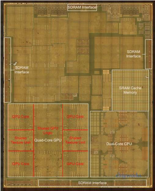
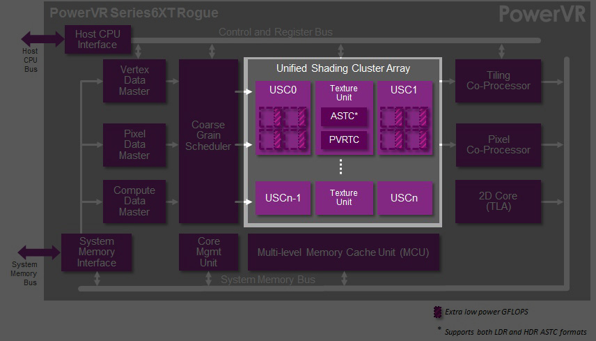
A close analysis of the die shot makes it clear that there are only 4 GPU cores available and not 6, which immediately rules out the 6 core GX6650 we were previously expecting. Instead with 4 cores present this is conclusive proof that Apple is using the smaller 4 core GX6450 on A8, the direct successor to the G6430 used on the A7. GX6450 induces some performance optimizations along with some feature updates – including ASTC support, which Apple’s documentation has already confirmed is present – so its inclusion here is a natural progression for Apple.
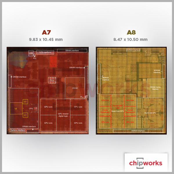
On A8 and its 20nm process this measures at 19.1mm2, versus A7’s 22.1mm2 G6430. As a result Apple is saving some die space compared to A7, but this is being partially offset by the greater complexity of GX6450 and possibly additional SRAM for larger caches on the GPU. Meanwhile looking at the symmetry of the block, it’s interesting that the blocks of texturing resources that every pair of GPU cores share is so visible and so large. With these resources being so big relative to the GPU cores themselves, you can see why Imagination would want to share them as opposed to building them 1:1 with the GPU cores.
Meanwhile opposite the GPU we have the CPU block. Unlike the GPU the CPU block has seen some significant shrinking, which Chipworks estimates is down from 17.1mm2 in A7 to 12.2mm2 in A8. In A7 Cyclone did not lend itself to easily picking apart the individual CPU cores, and neither does the CPU here in A8. We’ll be looking at the new CPU’s architecture in-depth in our iPhone 6 review, but for now it’s safe to say that while this is definitely derived from Cyclone, Apple has added a few tweaks over the last year that make it an even more potent CPU than the first Cyclone. Meanwhile based on this die shot Chipworks believes that the L2 cache has been reorganized to a per-core design, as there is no obvious single block of L2 on A8 like there was A7.

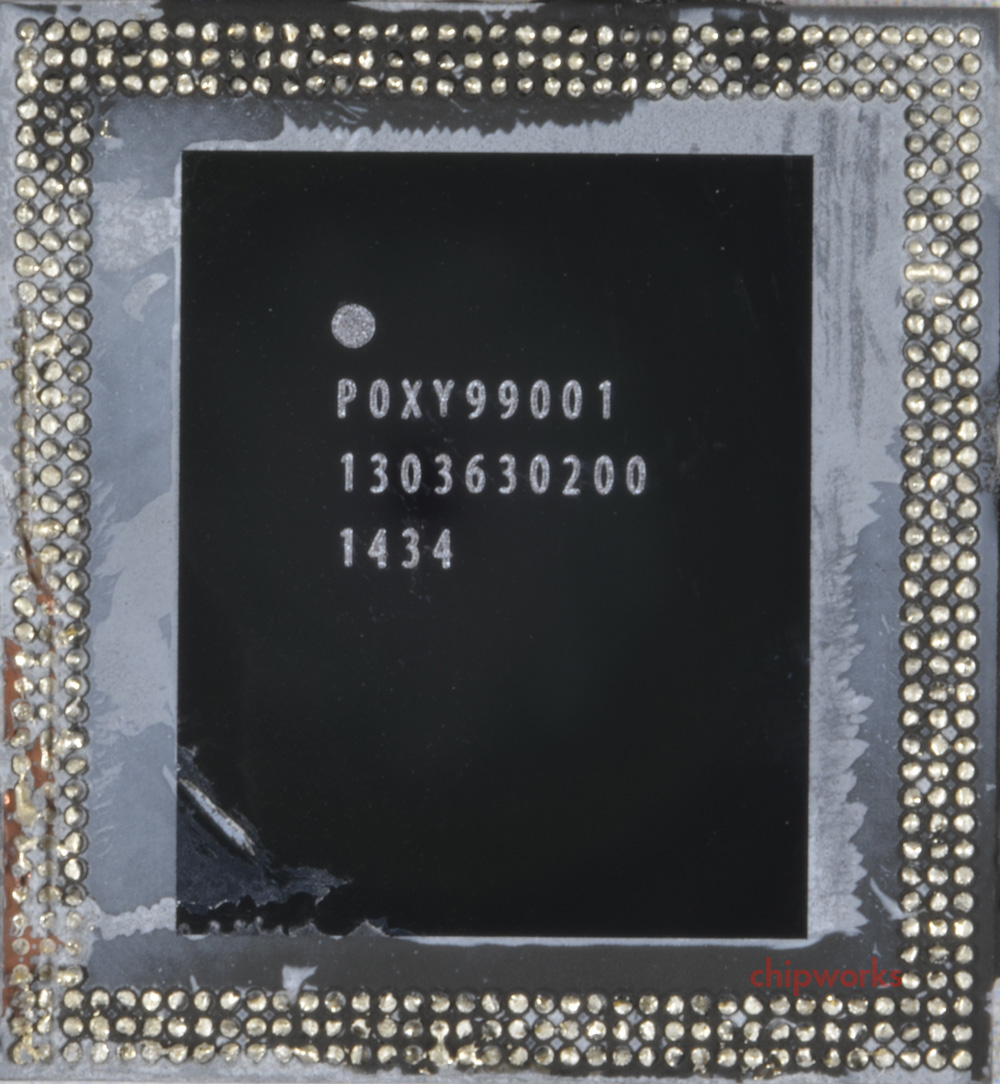
A8 With PoP DRAM Removed
The final major identifiable block on A8 is once again the SRAM cache memory. On A7 we discovered that this block was 4MB and was responsible for servicing the GPU and CPU. On A8 this block is similarly present and serving the same role. This 4MB of SRAM ends up being quite big despite the shrink from 28nm to 20nm, and while at first glance it seems like it should be larger than 4MB given the relative size, in practice what has happened is that the individual SRAM cells have not shrunk by a full 50%. Chipworks estimates the cell size to now be about 0.08µm2, versus 0.12µm2 on A7, which is closer to a 33% shrink that a 50% shrink. As a result the SRAM cache still takes up a fair bit of space, but the value of being able to serve larger memory requests without having to go off-die continues to be immense.
Apple A8 vs A7 SoCs
 Apple A8 (2014)Apple A7 (2013)
Manufacturing ProcessTSMC 20nm HKMGSamsung 28nm HKMG
Die Size89mm2104mm2
Transistor Count~2B"Over 1B"
CPU2 x Apple Enhanced Cyclone ARMv8 64-bit cores2 x Apple Cyclone ARMv8 64-bit cores
GPUIMG PowerVR GX6450IMG PowerVR G6430
Overall, Chipworks’ analysis points to A8 being fabbed on TSMC’s 20nm process. This makes A8 among the first SoCs to receive the 20nm treatment. Thanks to this smaller node Apple has been able to build in additional features to the SoC while simultaneously shaving off around 15% of their die size. Chipworks estimates the final die size of A8 to stand at 89mm2, versus the 104mm2 for the Samsung 28nm based A7. Chipworks notes that if this were a straight shrink that one would expect the A8 to be closer to 50% the size of A7 (though not all logic can shrink quite that well), which indicates that Apple has spent quite a bit of die size on improving performance through more complex CPU and GPU architectures and miscellaneous feature additions.
Wrapping things up, we’ll be back later this month with our review of the iPhone 6 family and our full analysis of the A8 SoC. So until then stay tuned.

Monday, January 13, 2014

Apple A8 (Next Processor Chip)


The article below (and at the link) provides general background about Apple’s A8 competitive advantages.  Key benefits can be gleaned from Apples purchases of small companies (see September 2013 How Apple Leverages its R&D) would be an easier implementation of;


·         Security features such as secure TouchID, 
·         HDR photography,
·         face detection,
·         and iAds 


Ron
Insightful, timely, and accurate semiconductor consulting.
Semiconductor information and news at - http://www.maltiel-consulting.com/


Jan. 10, 2014 4:33 PM ET 

The move to 64-bit has been years in the making. But we did it because we wanted to put desktop-class processing power in the palm of people's hands. - Apple iPhone 5s design web page [emphasis added]
I began my article on the A7 chip from Apple (AAPL) with this quote from CEO Tim Cook, More...