Showing posts with label A7. Show all posts

Tuesday, May 26, 2015

Apple Propelled IC Growth to +60%/ +20%

My last blog (Semiconductor IC Sales +60% to +20% for 6 Companies) discusses large increase in semiconductor sales for some companies in first quarter of 2015.The driving force behind these large growth is Apple. Apple purchase more than $25B in 2014 (see table below). When Apple started diversifying its semiconductor sources it led to large impact on them. 


2013 Ranking

2014 Ranking


Company


2013


2014

Growth (%) 2013-2014

Market Share (%) 2014
1
1
Samsung 
30.6
32.1
5.1
9.4
2
2
Apple
23.5
25.8
9.8
7.6
3
3
HP
13.7
14.7
7.1
4.3
4
4
Lenovo
9.5
12.8
33.9
3.8
5
5
Dell
9.1
10.3
13.2
3.0
6
6
Sony
7.7
7.4
-2.8
2.2
9
7
Huawei
4.9
6.0
21.6
1.8
7
8
Cisco Systems
5.6
5.8
3.1
1.7
10
9
LG Electronics
4.7
5.5
15.9
1.6
8
10
Toshiba
5.5
5.3
-4.0
1.5


Others
200.2
214.2
7.0
63.0


Total
315.0
339.9
7.9
100.0
Note: Some columns do not add to totals shown because of rounding.
Source: Gartner (January 2015)

Apple demand is large part of TSMC 44% sales growth, GlobalFoundaries 21%, and Hynix 25% in first quarter of 2014.

Apple diversifying its semiconductor supplier started couple years ago (see November 2013 blog http://semiconductorexpert.blogspot.com/2013/11/who-will-fabricate-apple-microprocessors.html ).

When Apple shifted from using Samsung as the only vendor fabricating its microprocessor, it had large impact on Samsung sales. Apple was a major customer of Samsung several years ago. See March 2012 blog Foundry Rankings (Including Samsung’s  iPad, iPhone Breakdown) . 

More about Apple increases reliance on TSMC and adding GlobalFoundaries is in earlier blogs such as April 2015 Next iPhone Be Fabricated at TSMC .


Ron
Insightful, timely, and accurate semiconductor consulting.
Semiconductor information and news at - 
http://www.maltiel-consulting.com/

Monday, February 2, 2015

Samsung, Apple's iPhone, and Fabs Consolidation

The increasing cost of semiconductor fabrication has led to consolidation of fabs over the last few years (see March 2012 Moore's Law End? (Next semiconductors gen. cost $10 billion)

At the same time Apple was facing the risk of depending on a single semiconductor fabrication source ( Foundry Rankings (Including Samsungs' iPad, iPhone Breakdown).

It makes sense for Apple to diversify its chip production as discussed below.

"KGI Research predicted that Samsung would end up producing around 75 percent of the A9 chips with Global Foundry manufacturing the rest...
Another report from BusinessKorea .. Apple would be using Samsung almost exclusively for manufacturing NAND flash storage, RAM and batteries for the upcoming iPhone 6s and the Apple Watch."

See also report of Apple's A9 production using Samsung's 14nm FinFET made by both Samsung and GlobalFoundaries (Samsung-GlobalFoundries deal gives Apple’s chip production greater flexibility

Another benefit for Apple is control of its chips price supplied by using more than one vendor.


Ron
Insightful, timely, and accurate semiconductor consulting.
Semiconductor information and news at - http://www.maltiel-consulting.com/


iPhone 7, iPad 2015 Specs News: Apple Seen Picking Samsung To Manufacture Most A9 Chips For New iPhones, iPads

YOUTUBE/APPLE
The A8 chip.
Rumors swirling around Apple's new devices in its iPhone and iPad ranges continue, with the latest concerning what type of chip will be used. All recent rumors pointed towards Samsung winning the contract to manufacture the bulk of the new A9 chips, which will be at the heart of the new iPhones and iPads.
Initially, it was reported that Taiwan Semiconductor Manufacturing Company had won the contract and would be manufacturing most of the A9 chips. However, soon after another report stated that instead of the Taiwan company, Samsung had been contracted to supply most of the A9 and A9X chips that would be used on the new iPhones and iPads.
With no official confirmation on the subject, speculations have increased on the company that would eventually produce the new Apple chip. In a recent statement, Samsung declined to provide any information, saying that "it does not comment on market speculation"
A report by KGI Research predicted that Samsung would end up producing around 75 percent of the A9 chips with Global Foundry manufacturing the rest. This report followed an earlier note by KGI Research that pointed towards Apple spreading out the production of the chip among the Taiwan semiconductor company, Samsung, Qualcomm, Global Foundry and Intel. It also hinted that Apple had tapped Samsung for manufacturing the S1 chips which will be featured in the upcoming Apple Watch. As for the Taiwan company, it will be more involved in producing the S2 chip which will be used in future versions of the Apple Watch.
Another report from BusinessKorea last month stated that Apple would be using Samsung almost exclusively for manufacturing NAND flash storage, RAM and batteries for the upcoming iPhone 6s and the Apple Watch.
While all these reports are speculations at this point, several research houses have noted that Apple is looking to engage many suppliers to produce the A9 chip in order to minimize any risks involved.

Wednesday, September 24, 2014

Apple's iPhone 6 A8 Teardown

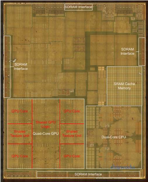
Chipworks has been quick to teardown Apple's A8 processor, which is the secret sauce driving the new iPhone 6. Some details of the teardown are discussed below.

"Apple has spent quite a bit of die size on improving performance through more complex CPU and GPU architectures and miscellaneous feature additions."


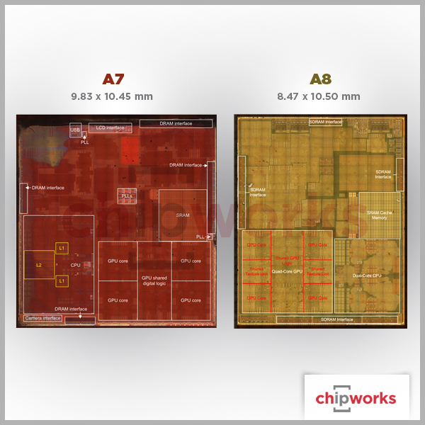
A8 is fabricated on TSMC 20nm process while  A7 was manufactured on Samsung 28nm process. Shrinking the transistors gate to 20nm enables the CPU to operate faster. While limiting A8 to 4 GPU cores and not 6 help to reduce the new iPhone power.


Ron
Insightful, timely, and accurate semiconductor consulting.
Semiconductor information and news at - http://www.maltiel-consultin


Chipworks Disassembles Apple's A8 SoC: GX6450, 4MB L3 Cache & More

by Ryan Smith on September 23, 2014 1:00 PM EST

One of the more enjoyable rituals with Apple’s annual iPhone launch is the decapping, deconstruction, and photographing of the processor die at the heart of Apple’s newest SoC.  While we can learn a lot about the SoC from software, for some things there’s just no replacement for looking at the hardware itself and counting the functional blocks present. And this year, as in past years, the honor of being the first to tear apart the SoC goes to Chipworks.
For determining the layout of A8, Chipworks reached out to us to solicit our input on their die shot, and after some rounds of going back and forth we believe we’ve come to a solid determination of some of A8’s features and how it has been configured. So let's dive in.
First and foremost we’ll start with A8’s GPU, as this was one of the hardest elements to analyze in software. Based on Apple’s 50% performance improvement we had previously speculated that A8 contained an Imagination PowerVR GX6650. However as we noted back then, a die shot would reveal all, and right on schedule it has.
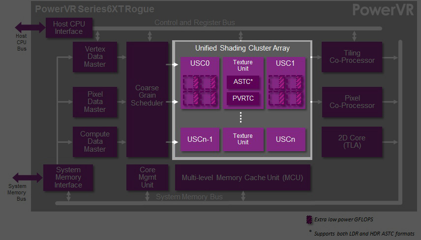
A close analysis of the die shot makes it clear that there are only 4 GPU cores available and not 6, which immediately rules out the 6 core GX6650 we were previously expecting. Instead with 4 cores present this is conclusive proof that Apple is using the smaller 4 core GX6450 on A8, the direct successor to the G6430 used on the A7. GX6450 induces some performance optimizations along with some feature updates – including ASTC support, which Apple’s documentation has already confirmed is present – so its inclusion here is a natural progression for Apple.
On A8 and its 20nm process this measures at 19.1mm2, versus A7’s 22.1mm2 G6430. As a result Apple is saving some die space compared to A7, but this is being partially offset by the greater complexity of GX6450 and possibly additional SRAM for larger caches on the GPU. Meanwhile looking at the symmetry of the block, it’s interesting that the blocks of texturing resources that every pair of GPU cores share is so visible and so large. With these resources being so big relative to the GPU cores themselves, you can see why Imagination would want to share them as opposed to building them 1:1 with the GPU cores.
Meanwhile opposite the GPU we have the CPU block. Unlike the GPU the CPU block has seen some significant shrinking, which Chipworks estimates is down from 17.1mm2 in A7 to 12.2mm2 in A8. In A7 Cyclone did not lend itself to easily picking apart the individual CPU cores, and neither does the CPU here in A8. We’ll be looking at the new CPU’s architecture in-depth in our iPhone 6 review, but for now it’s safe to say that while this is definitely derived from Cyclone, Apple has added a few tweaks over the last year that make it an even more potent CPU than the first Cyclone. Meanwhile based on this die shot Chipworks believes that the L2 cache has been reorganized to a per-core design, as there is no obvious single block of L2 on A8 like there was A7.

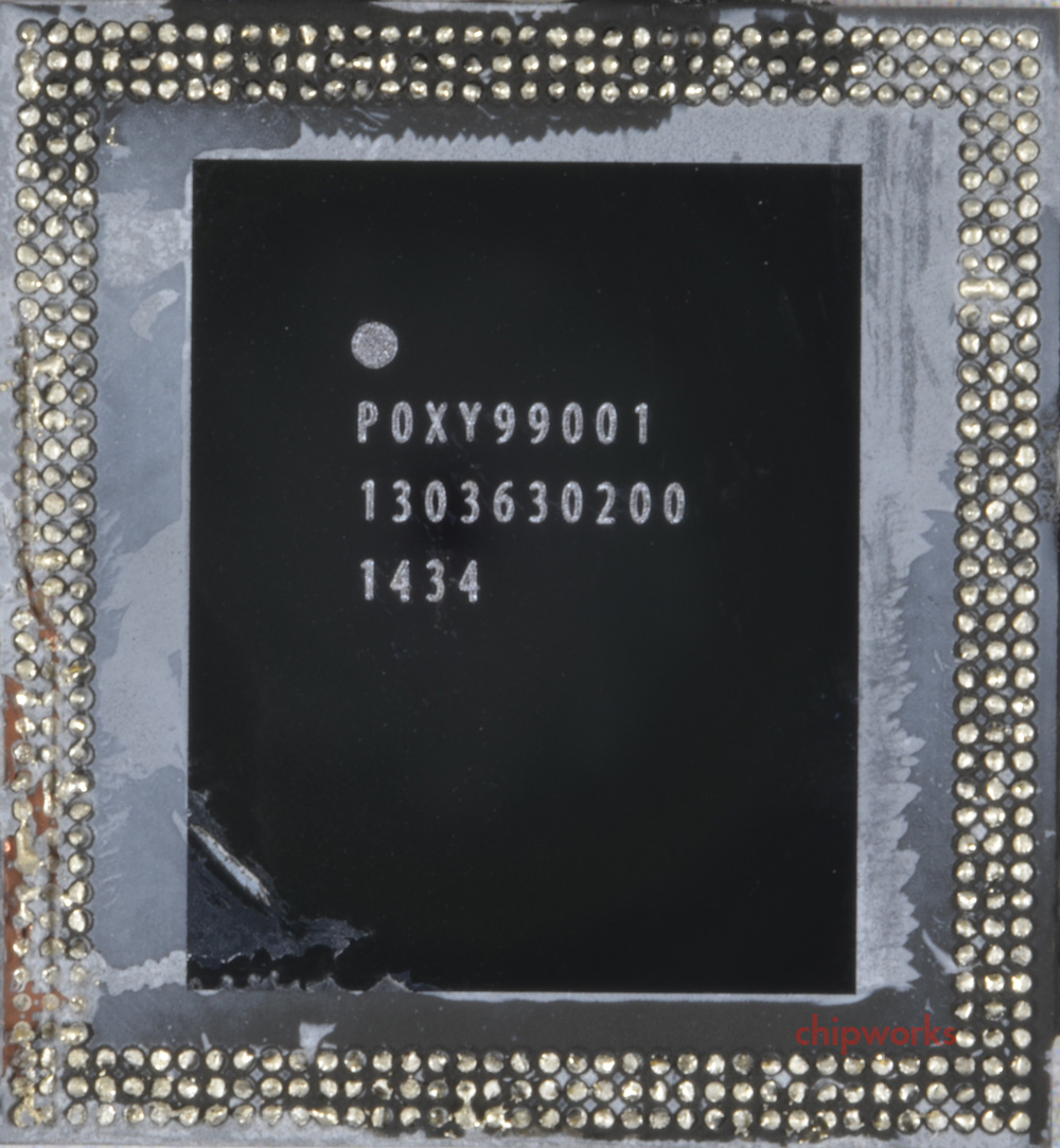
A8 With PoP DRAM Removed
The final major identifiable block on A8 is once again the SRAM cache memory. On A7 we discovered that this block was 4MB and was responsible for servicing the GPU and CPU. On A8 this block is similarly present and serving the same role. This 4MB of SRAM ends up being quite big despite the shrink from 28nm to 20nm, and while at first glance it seems like it should be larger than 4MB given the relative size, in practice what has happened is that the individual SRAM cells have not shrunk by a full 50%. Chipworks estimates the cell size to now be about 0.08µm2, versus 0.12µm2 on A7, which is closer to a 33% shrink that a 50% shrink. As a result the SRAM cache still takes up a fair bit of space, but the value of being able to serve larger memory requests without having to go off-die continues to be immense.
Apple A8 vs A7 SoCs
 Apple A8 (2014)Apple A7 (2013)
Manufacturing ProcessTSMC 20nm HKMGSamsung 28nm HKMG
Die Size89mm2104mm2
Transistor Count~2B"Over 1B"
CPU2 x Apple Enhanced Cyclone ARMv8 64-bit cores2 x Apple Cyclone ARMv8 64-bit cores
GPUIMG PowerVR GX6450IMG PowerVR G6430
Overall, Chipworks’ analysis points to A8 being fabbed on TSMC’s 20nm process. This makes A8 among the first SoCs to receive the 20nm treatment. Thanks to this smaller node Apple has been able to build in additional features to the SoC while simultaneously shaving off around 15% of their die size. Chipworks estimates the final die size of A8 to stand at 89mm2, versus the 104mm2 for the Samsung 28nm based A7. Chipworks notes that if this were a straight shrink that one would expect the A8 to be closer to 50% the size of A7 (though not all logic can shrink quite that well), which indicates that Apple has spent quite a bit of die size on improving performance through more complex CPU and GPU architectures and miscellaneous feature additions.
Wrapping things up, we’ll be back later this month with our review of the iPhone 6 family and our full analysis of the A8 SoC. So until then stay tuned.