Showing posts with label CPU. Show all posts

Wednesday, September 24, 2014

Apple's iPhone 6 A8 Teardown

Chipworks has been quick to teardown Apple's A8 processor, which is the secret sauce driving the new iPhone 6. Some details of the teardown are discussed below.

"Apple has spent quite a bit of die size on improving performance through more complex CPU and GPU architectures and miscellaneous feature additions."


A8 is fabricated on TSMC 20nm process while  A7 was manufactured on Samsung 28nm process. Shrinking the transistors gate to 20nm enables the CPU to operate faster. While limiting A8 to 4 GPU cores and not 6 help to reduce the new iPhone power.


Ron
Insightful, timely, and accurate semiconductor consulting.
Semiconductor information and news at - http://www.maltiel-consultin


Chipworks Disassembles Apple's A8 SoC: GX6450, 4MB L3 Cache & More

by Ryan Smith on September 23, 2014 1:00 PM EST

One of the more enjoyable rituals with Apple’s annual iPhone launch is the decapping, deconstruction, and photographing of the processor die at the heart of Apple’s newest SoC.  While we can learn a lot about the SoC from software, for some things there’s just no replacement for looking at the hardware itself and counting the functional blocks present. And this year, as in past years, the honor of being the first to tear apart the SoC goes to Chipworks.
For determining the layout of A8, Chipworks reached out to us to solicit our input on their die shot, and after some rounds of going back and forth we believe we’ve come to a solid determination of some of A8’s features and how it has been configured. So let's dive in.
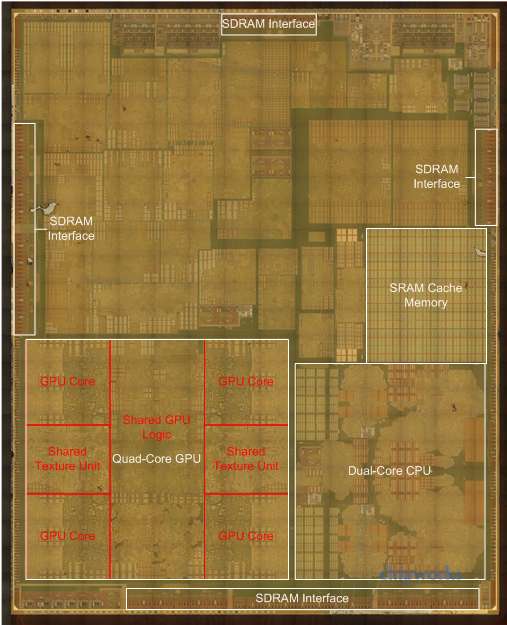
First and foremost we’ll start with A8’s GPU, as this was one of the hardest elements to analyze in software. Based on Apple’s 50% performance improvement we had previously speculated that A8 contained an Imagination PowerVR GX6650. However as we noted back then, a die shot would reveal all, and right on schedule it has.
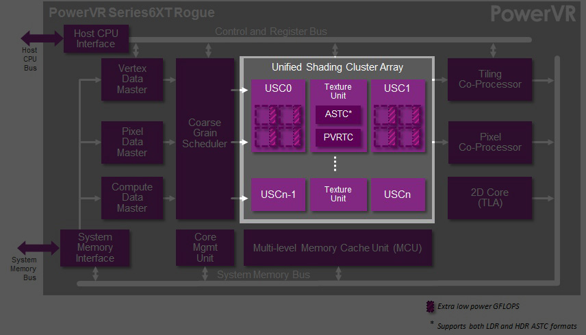
A close analysis of the die shot makes it clear that there are only 4 GPU cores available and not 6, which immediately rules out the 6 core GX6650 we were previously expecting. Instead with 4 cores present this is conclusive proof that Apple is using the smaller 4 core GX6450 on A8, the direct successor to the G6430 used on the A7. GX6450 induces some performance optimizations along with some feature updates – including ASTC support, which Apple’s documentation has already confirmed is present – so its inclusion here is a natural progression for Apple.
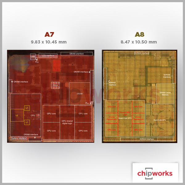
On A8 and its 20nm process this measures at 19.1mm2, versus A7’s 22.1mm2 G6430. As a result Apple is saving some die space compared to A7, but this is being partially offset by the greater complexity of GX6450 and possibly additional SRAM for larger caches on the GPU. Meanwhile looking at the symmetry of the block, it’s interesting that the blocks of texturing resources that every pair of GPU cores share is so visible and so large. With these resources being so big relative to the GPU cores themselves, you can see why Imagination would want to share them as opposed to building them 1:1 with the GPU cores.
Meanwhile opposite the GPU we have the CPU block. Unlike the GPU the CPU block has seen some significant shrinking, which Chipworks estimates is down from 17.1mm2 in A7 to 12.2mm2 in A8. In A7 Cyclone did not lend itself to easily picking apart the individual CPU cores, and neither does the CPU here in A8. We’ll be looking at the new CPU’s architecture in-depth in our iPhone 6 review, but for now it’s safe to say that while this is definitely derived from Cyclone, Apple has added a few tweaks over the last year that make it an even more potent CPU than the first Cyclone. Meanwhile based on this die shot Chipworks believes that the L2 cache has been reorganized to a per-core design, as there is no obvious single block of L2 on A8 like there was A7.
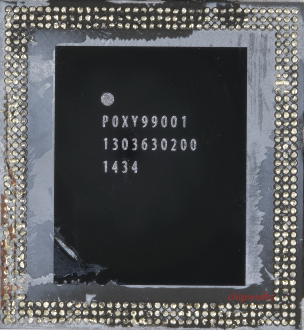
A8 With PoP DRAM Removed
The final major identifiable block on A8 is once again the SRAM cache memory. On A7 we discovered that this block was 4MB and was responsible for servicing the GPU and CPU. On A8 this block is similarly present and serving the same role. This 4MB of SRAM ends up being quite big despite the shrink from 28nm to 20nm, and while at first glance it seems like it should be larger than 4MB given the relative size, in practice what has happened is that the individual SRAM cells have not shrunk by a full 50%. Chipworks estimates the cell size to now be about 0.08µm2, versus 0.12µm2 on A7, which is closer to a 33% shrink that a 50% shrink. As a result the SRAM cache still takes up a fair bit of space, but the value of being able to serve larger memory requests without having to go off-die continues to be immense.
Apple A8 vs A7 SoCs
 Apple A8 (2014)Apple A7 (2013)
Manufacturing ProcessTSMC 20nm HKMGSamsung 28nm HKMG
Die Size89mm2104mm2
Transistor Count~2B"Over 1B"
CPU2 x Apple Enhanced Cyclone ARMv8 64-bit cores2 x Apple Cyclone ARMv8 64-bit cores
GPUIMG PowerVR GX6450IMG PowerVR G6430
Overall, Chipworks’ analysis points to A8 being fabbed on TSMC’s 20nm process. This makes A8 among the first SoCs to receive the 20nm treatment. Thanks to this smaller node Apple has been able to build in additional features to the SoC while simultaneously shaving off around 15% of their die size. Chipworks estimates the final die size of A8 to stand at 89mm2, versus the 104mm2 for the Samsung 28nm based A7. Chipworks notes that if this were a straight shrink that one would expect the A8 to be closer to 50% the size of A7 (though not all logic can shrink quite that well), which indicates that Apple has spent quite a bit of die size on improving performance through more complex CPU and GPU architectures and miscellaneous feature additions.
Wrapping things up, we’ll be back later this month with our review of the iPhone 6 family and our full analysis of the A8 SoC. So until then stay tuned.
Monday, July 21, 2014

Bottlenecks: DRAM & Moore's Law

In addition to Moore's law slowing there are bottlenecks between the memory device and the CPU. 


The article below discusses
" How long will it will it take to find a technology so fundamentally different and better from anything we have today that we can do away with the DRAM latency and power consumption bottleneck?

There is a need for -
"A new RAM technology that cut main memory accesses by an order of magnitude would be reason enough to reevaluate the entire balance of resources on a microprocessor. If accessing main memory was as fast as accessing the CPUs cache, you might not need cache on the CPU die or package at all — or at least, you wouldn't need anything beyond L1 and maybe a small L2."

More about Moore's Law bottleneck from March 2012 Moore's Law End? (Next semiconductors gen. cost $10 billion)

Ron
Insightful, timely, and accurate semiconductor consulting.
Semiconductor information and news at - 
http://www.maltiel-consulting.com/


DRAM is pretty amazing stuff. The basic structure of the RAM we still use today was invented more than forty years ago and, just like its CPU cousin, it has continually benefited from the huge improvements that have been made in fabrication technology and density improvements. Less than ten years ago, 2GB of RAM was considered plenty for a typical desktop system — today, a high-end smartphone offers the same amount of memory but at a fifth of the power consumption.
After decades of scaling, however, modern DRAM is starting to hit a brick wall. Much in the same way that the CPU gigahertz race ran out of steam, the high latency and power consumption of DRAM is one of the most significant bottlenecks in modern computing. As supercomputers move towards exascale, there are serious doubts about whether DRAM is actually up to the task, or whether a whole new memory technology is required. Clearly there are some profound challenges ahead — and there’s disagreement about how to meet them.

What’s really wrong with DRAM?

A few days ago, Vice ran an article that actually does a pretty good job of talking about potential advances in the memory market, but includes a graph I think is fundamentally misleading. That’s not to sling mud at Vice — do a quick Google search, and you’ll find this picture has plenty of company:
DRAM scaling
The point of this image is ostensibly to demonstrate how DRAM performance has grown at a much slower rate than CPU performance, thereby creating an unbridgeable gap between the two system. The problem is, this graph no longer properly illustrates CPU performance or the relationship between it and memory.  Moore’s law has stopped functioning at anything like its historic level for CPUs or DRAM, and “memory performance” is simply too vague to accurately describe the problem.
The first thing to understand is that modern systems have vastly improved the bandwidth-per-core ratio compared to where we sat 14 years ago. In 2000, a fast P3 or Athlon system had a 64-bit memory bus connected to an off-die memory controller clocked at 133MHz. Peak bandwidth was 1.06GB/s while CPU clocks were hitting 1GHz. Today, a modern processor from AMD or Intel is clocked between 3-4GHz, while modern RAM is running at 1066MHz (2133MHz effective for DDR3) — or around 10GB/sec peak. Meanwhile we’ve long since started adding multiple memory channels, brought the memory controller on die, and clocked it at full CPU speed as well.
ddr_memory_data_rate
The problem isn’t memory bandwidth — it’s memory latency and memory power consumption. As we’ve previously discussed, DDR4 actually moves the dial backwards as far as the former is concerned, while improving the latter only modestly. It now looks as though the first generation of DDR4 will have some profoundly terrible latency characteristics; Micron is selling DDR4-2133 timed at 15-15-15-50. For comparison, DDR3-2133 can be bought at 11-11-11-27 — and that’s not even highest-end premium RAM. This latency hit means DDR4 won’t actually match DDR3′s performance for quite some time, as shown here:

This is where the original graph does have a point — latency has only improved modestly over the years, and we’ll be using DDR4-3200 before we get back to DDR3-1600 latencies. That’s an obvious issue — but it’s actually not the problem that’s holding exascale back. The problem for exascale is that DRAM power consumption is currently much too high for an exascale system.
The current goal is to build an exascale supercomputer within a 20MW power envelope,sometime between 2018 and 2020. Exascale describes a system that has exaflops of processing power, and perhaps hundreds of petabytes of RAM (current systems max out at around 30 petaflops and only a couple of petabytes of RAM. If today’s best DDR3 were used for the first exascale systems, the DRAM alone would consume 54MW of power. Clearly massive improvements are needed. So how do we find them?

Reinvent the wheel — or iterate like crazy

There are two ways to attack this problem, and they both have their proponents. One method is to keep building on the existing approaches that have given us DDR4 and the Hybrid Memory Cube. It’s reasonably likely that we can squeeze a great deal of additional improvement out of the basic DRAM structure by stacking dies, further optimizing trace layouts, using through-silicon vias (TSVs), and adapting 3D designs. According to a recent research paper, this could cut the RAM power consumption of a 100-petabyte supercomputer from 52MW (assuming standard DDR3-1333) to well below 10MW depending on the precise details of the technology.
While 100PB  is just one tenth of the way to exascale, reducing the RAM’s power consumption by an order of magnitude is unquestionably on the right track.
DRAM-Types
The other, more profound challenge, is the idea of finding a complete DRAM replacement. You may have noticed that while we cover new approaches and alternatives to conventional storage technologies, virtually all the proposed methods address the shortcomings of NAND storage — not DRAM. There’s a good reason for that — DRAM has survived more than 40 years precisely because it’s been very, very hard to beat.
The argument for reinventing the wheel is anchored in concepts like memristors, MRAM,FeRAM, and a host of other potential next-generation technologies. Some of them have the potential to replace DRAM altogether, while others, like phase change memory, would be used as a further buffer between DRAM and NAND. The big-picture fact that Vice does get right is that discovering a new memory technology that was faster and lower power than DRAM really would change the fundamental nature of computing — over time.
It’s easy to forget that the trends we’re talking about today have literally been true for decades. 11 years ago, computer scientist David Patterson presented a paper entitledLatency Lags Bandwidth, in which he measured the improvements in bandwidth against data accesses across CPUs, DRAM, LAN, and hard drives (SSDs weren’t a thing at that time). What he found is summarized below:
Latency lags bandwidth
In every case — and in a remarkably consistent fashion — latency improved by 20-30% in the same time that it took bandwidth to double. This problem is one we’ve been dealing with for decades — it’s been addressed via branch prediction, instruction sets, and ever-expanding caches. It’s been observed that we add one layer of cache roughly every 10 years, and we’re on track to keep that with Intel’s 128MB EDRAM cache on certain Haswell processors.
A new main memory with even half standard DRAM latency would give programmers an opportunity to revisit decades of assumptions about how microprocessors should be built. A new RAM technology that cut main memory accesses by an order of magnitude would be reason enough to reevaluate the entire balance of resources on a microprocessor. If accessing main memory was as fast as accessing the CPUs cache, you might not needcache on the CPU die or package at all — or at least, you wouldn’t need anything beyond L1 and maybe a small L2.
How long will it will it take to find a technology so fundamentally different and better from anything we have today that we can do away with the DRAM latency and power consumption bottleneck? Given how such a fundamental breakthrough would be vital to our ability to reach exascale computing and beyond, though, I hope it’s soon.

Monday, February 24, 2014

Qualcom, MediaTek Processor Chip Race

Apple 64 bit CPU used in its cell phones (see September 2013 iPhone 5s $199 Manufacturing Cost (BOM)) led Qualcomm to advance to 4 and 8 core Snapdragon processor with 64 bit support (see below).


Similarly, MediaTek, a chipset manufacturer based out of Taiwan, has been making some huge moves lately. Just over two months ago, it came out with the "world's first true octa-core" processor, which consisted of eight Cortex-A7 cores capable of operating simultaneously. Now that ARM has announced Cortex-A17 technology, (see second article below).

More about MediaTek see July 2013 Smartphone: MediaTek Overtaking Qulacomm


Ron
Insightful, timely, and accurate semiconductor consulting.
Semiconductor information and news at - http://www.maltiel-consulting.com/


Qualcomm’s 4- and 8-core Snapdragon 610 and 615 trade CPU power for 64-bit

Cortex A53 won't stand up to Krait, but Qualcomm adds a capable GPU to the mix.


The Snapdragon 610 will be equipped with four ARM Cortex A53 CPU cores running at an unspecified clock speed, rather than one of Qualcomm's custom ARM architectures. Snapdragon 615 takes a classic more-is-better approach, adding four more Cortex A53 CPU cores to the 610 for a total of eight. (Update:According to AnandTech, each group of four cores in the Snapdragon 615 will be optimized for a different performance level. One group will offer faster performance and one will offer lower power consumption, but both groups can theoretically be active at the same time.) For reference, the original Snapdragon 600 included four 32-bit Krait 300 CPU cores running at 1.7 or 1.9GHz, depending on the specific model.Qualcomm's first 64-bit chip wasn't a record-breaking high-end Snapdragon, but rather the modest, mid-range Snapdragon 410. Today at the Mobile World Congress in Barcelona, the company announced its next two 64-bit mobile SoCs, the Snapdragon 610 and 615. Rather than introducing 64-bit at the top of its product lineup and letting it trickle down, Qualcomm seems to be taking the opposite approach.
The list of CPU architectures that ARM offers is getting difficult to keep track of, but here's what you need to know: Cortex A53 is a replacement of sorts for the Cortex A7. It's the first of two CPU designs from ARM that supports the new, more efficient ARMv8 instruction set and, by extension, the traditional benefits of a 64-bit architecture (not all ARMv8 chips are 64-bit, but everything we've seen so far has been). Cortex A7 and A53 are both small cores designed for low power rather than high performance, which means that Snapdragon 610 and 615 may actually be slower than last year's Snapdragon 600 for many tasks. For software that can use all of the CPU cores at once, it's possible that the eight-core 615 will be able to gain an edge, but the CPUs will likely be more remarkable for their ARMv8 support than their raw performance.
Luckily for Qualcomm, the chips' custom GPUs and LTE modems will be more compelling for partners and consumers (and will differentiate the 610 and 615 from theSnapdragon 410, which also uses four Cortex A53 CPU cores). The Adreno 405 GPU is a relative of the Adreno 420 in the upcoming Snapdragon 805, and while it will probably be a little slower, it still supports OpenGL ES 3.0 (also included in Adreno 300 GPUs), DirectX 11.2 (good for Windows phones), H.265 video decoding, and displays up to 2560×1600 in resolution.
On the wireless side, the 610 and 615 support LTE speeds of up to 150Mbps and are compatible with Qualcomm's "RF360 Front End Solution," which allows phone manufacturers to support multiple worldwide LTE bands with a single phone rather than having to customize multiple configurations for different markets. Bluetooth 4.1 and 802.11ac Wi-Fi are also included.
Qualcomm says that the 410, 610, and 615 will all be supported by the same software and will be pin-compatible, meaning that any phone designed for one of these three chips can be upgraded or downgraded at will. This should be handy for OEMs looking to spruce up an older handset, or phone-makers who want to experiment a bit to find the best balance between performance, power consumption, and cost.
Both the Snapdragon 610 and 615 are scheduled to begin sampling in the third quarter of 2014 and will appear in shipping phones and tablets in the fourth quarter; the Snapdragon 410 and 805 are scheduled to be released in a similar timeframe. Those of you waiting for a true high-end 64-bit part from Qualcomm will have to keep waiting. The new-ish Snapdragon 801 and the Snapdragon 805 will be the company's flagship SoCs through the end of 2014, but by the end of the year we'd expect to hear something about some kind of 64-bit Snapdragon 810-series part based on either the high-performance Cortex A57 architecture or a new version of Qualcomm's custom Krait architecture.

MediaTek, a chipset manufacturer based out of Taiwan, has been making some huge moves lately. Just over two months ago, it came out with the "world's first true octa-core" processor, which consisted of eight Cortex-A7 cores capable of operating simultaneously. Now that ARM has announced Cortex-A17 technology, however, MediaTek is ready to start sampling a new octa-core chip that consists of four 2.2-2.5GHz A17 cores and four 1.7GHz A7s, and comes with a Rogue PowerVR Series6 GPU to take care of any graphical needs you might have.
As an aside, the A17 cores come with a 60 percent improvement in performance over the current-gen A9s, and are primarily designed to make midrange smartphones and tablets even faster. That said, MediaTek tells us that its new chips, known as the MT6595, are actually meant to be featured in premium devices and will square off directly against Qualcomm's Snapdragon 800 and 805. And it's certainly got a few noteworthy features: first, the chip will use ARM's big.LITTLE architecture and Heterogeneous Multi-Processing, which means you can use all eight cores for the most intense tasks, or you can use just one or two at a time for incredibly basic activities. The company claims that this chip will be faster and more power efficient than the octa-core Exynos options, which feature four A15 cores and four A7s at lower frequencies.
Additionally, the MT6595 claims to be the first octa-core LTE system-on-chip with an H.265 Ultra HD Codec built-in to the platform, which offers 4K2K video recording and playback capabilities. In much the same way that most manufacturers don't enable all of a chip's features, however, it'll be up to each individual company to add it in. The chips will begin sampling to phone makers and carriers in the first half of this year, and it's expected to arrive in products during the second half. And while it should find its way into smartphones and tablets around the world, MediaTek wants the MT6595 to enjoy a huge presence in the US.