Friday, December 27, 2013

3D Semiconductors-TSV w/ DRAM Memory

 Four High Bandwidth Memory stacks on one integrated chip.


Hynix just announced System in Package (SIP) on a single circuit board by combining 4 stacked DRAM using Through-Silicon Via (TSV) with AMD graphic chip (see below).

Hynix is trying to advance 3D manufacturing using TSV. TSV is essentially advanced packaging manufacturing where holes are drilled through each chip to connect them electrically when they are stacked on top of each other.

More about Through-Silicon Via (TSV) Introduction - 3D Integration & Through Silicon Via(TSV) and The future of computers: 3D chip stacking

While Samsung announced  in August 3D NAND using 3D during the chip manufacturing 1Tb SSD: 3D Vertical NAND


Ron
Insightful, timely, and accurate semiconductor consulting.
Semiconductor information and news at - http://www.maltiel-consulting.com/


Moore’s Law

SK Hynix Develops 4x Faster DRAM


SK Hynix reported on December 26th that it has developed the industry’s first High Bandwidth Memory (HBM) DRAM, using Through-Silicon Via (TSV) chip packaging technology.
TSV is a method of transmitting electrical signals through chips by way of creating an electrode that vertically passes through two or more chips, enhancing performance efficiency and reducing chip size.
The DRAM, which is undergoing review for standardization by the Joint Electron Device Engineering Council (JEDEC), is a high-performance, low-power, high-density memory product.  It only draws 1.2 volts of power per 1GB of data processed per second. Through its 1,024 Input/Output Gateways it can transfer 128GB of data per second, about 4 times faster than GDDR5 with 40% less power required.
SK Hynix used TSV technology to stack 4 DRAM chips on top of each other, each chip only 20nm high. The company worked in conjunction with leading graphic chipset maker AMD to put the chips in a System in Package (SIP) on a single circuit board.
The product is projected to be used in the graphics-heavy high-performance market, with future applications in supercomputer networks and servers.
More

Monday, November 25, 2013

Xbox, PlayStation 4 $332 Manufacturing Cost


TechInsights Teardown (see below) shows that both vendors used many similar parts to optimize their investment in the next generation of gaming consoles.

Based on iFixit tear down I believe that the tear down has a minor error that would add about $3 to Xbox cost of manufacturing due to the 8GB EMMC NAND flash being used instead of:  

"Xbox One also has 4GB eMMC NAND flash, making the non-volatile category US$3 higher for Xbox One"


"One interesting component is an 8GB chunk of eMMC NAND flash memory, the purpose of which Microsoft discussed last month with Eurogamer. In the words of Microsoft Technical Fellow Andrew Goossen:

We use it as a cache system-side to improve system response and again not disturb system performance on the titles running underneath. So what it does is that it makes our boot times faster when you're not coming out of the sleep mode—if you're doing the cold boot. It caches the operating system on there. It also caches system data on there while you're actually running the titles and when you have the snap applications running concurrently. It's so that we're not going and hitting the hard disk at the same time that the title is. All the game data is on the HDD. We wanted to be moving that head around and not worrying about the system coming in and monkeying with the head at an inopportune time.”

 Ron

Insightful, timely, and accurate semiconductor consulting.
Semiconductor information and news at - http://www.maltiel-consulting.com/


Teardown.com compares PlayStation 4 vs. Xbox One


TechInsights has performed a Quick Turn Teardown of the Sony PlayStation 4 and the Microsoft Xbox One.
TechInsights Teardown shows that both vendors used many similar parts to optimise their investment in the next generation of gaming consoles.
While AMD came out as a big winner in the APU (integrated CPU and GPU) there are choice design differences around the both the processor design and the use of memory in each device.
The TechInsights bill of materials (BOM) for the Microsoft Xbox One amounts to US$331.00. Based on this – and when the estimated costs for the peripherals are included – TechInsights believes Microsoft will have a gross profit of approximately US$100.00 per console sold. This is far better than the US$43.00 Sony will make per complete unit.
Says Al Cowsky, Costing Director, TechInsights: “At the console level, the Xbox One is US$10 less expensive than the PS4. This is primarily due to a US$23 memory premium on the PS4, but it is offset by an US$11 cost premium on the Xbox One processor.
"The Xbox One also has 4GB eMMC NAND flash, making the non-volatile category US$3 higher for Xbox One, while the housings/mechanicals of the Xbox One add another US$4 premium over the PS4.
"The Xbox One also comes with a Kinect vision system in-box with an estimated cost of US$39. This is more than made up for by the US$100 list price premium. Likewise, PS4 has an optional vision system accessory available for a list price of US$60 (unit not costed at this time)”
Xbox one Quick cost estimate
PS4 cost estimate

Friday, November 22, 2013

Facebook: Flash Storage in Database

Facebook continue to propel flash NAND memory usage in server and storage through open source implementations. See below more details on Flash Based Database.
“With the advent of flash storage, we are starting to see newer applications that can access data quickly by managing their own dataset on flash instead of accessing data over a network. These new applications are using what we call an embedded database.
“… When database requests are frequently served from memory or from very fast flash storage, network latency can slow the query response time. Accessing the network within a data center can take about 50 microseconds, as can fast-flash access latency. This means that accessing data over a network could potentially be twice as slow as an application accessing data locally. “
Additional technical details at Under the Hood: Building and open-sourcing RocksDB


More about Facebook Propels SSD Flash Storage


Ron
Insightful, timely, and accurate semiconductor consulting.
Semiconductor information and news at - http://www.maltiel-consulting.com/


Facebook’s latest open source effort: a flash-powereddatabase called RocksDB

by Derrick Harris


SUMMARY:

Facebook has open sourced a new embedded database called RocksDB that’s meant to take advantage of all the performance flash has to offer, from right on the application server. It might be a sign of best practices to come.

Facebook is on an open source roll lately, and on Thursday announced its latest open source project — an embedded key-value store called RocksDB. The company uses it to power certain user-facing applications that would suffer too much from having to access an external database over the network and to eliminate the certain problems relating to non-fully utilized IO performance on flash storage devices.

Facebook database engineer Dhruba Borthakur describes the design of and rationale behind RocksDB in some detail in a blog post, but the biggest factor leading to its creation might be the emergence of relatively inexpensive flash storage cards for servers (or, in Facebook’s case, custom-built servers packed entirely with flash).

“With the advent of flash storage, we are starting to see newer applications that can access data quickly by managing their own dataset on flash instead of accessing data over a network. These new applications are using what we call an embedded database.

“… When database requests are frequently served from memory or from very fast flash storage, network latency can slow the query response time. Accessing the network within a data center can take about 50 microseconds, as can fast-flash access latency. This means that accessing data over a network could potentially be twice as slow as an application accessing data locally. “

RocksDB was designed with these new hardware realities in mind, so it can take full advantage of the IOPS potential of flash memory as well as the computing power of many-core servers, Borthakur explains. Facebook has posted the results of a benchmark test running on a Fusion-io-powered server on the RocksDB GitHub page, and claims it’s significantly faster than Google’s LevelDB embedded key-value store.

From a broader IT perspective, RocksDB signals that the shifts in storage and computing economics that made the big data movement possible are now making their way into web application development, albeit using a storage media most organizations would consider using for storing “big data.” Facebook is performance hungry, but it’s also cost-sensitive, and it wouldn’t be storing “close to a petabyte of data across different applications,” as Borthakur writes, if the cost to do so was out of control.


He offered a handful of application types an embedded database like RocksDB is suitable for, including:

1. A user-facing application that stores the viewing history and state of users of a website.

2. A spam-detection application that needs fast access.

3. A graph-search query that needs to scan a data set in realtime.

4. RocksDB can be used to cache data from Hadoop, thereby allowing an app to query Hadoop data in realtime.

5. A message-queue that supports a high number of inserts and deletes.

In fact, Facebook has been finding all sorts of new ways to utilize flash as stepping stone between slow disks on one hand and expensive-but-fast RAM on the other.

Facebook is no doubt an early adopter of flash-heavy application architectures, but it’s also probably serving as a guiding light for other companies and their developers who want to achieve Facebook-like performance. As flash prices continue to drop — and now that Amazon Web Services is offering a whole suite of flash-backed instances on EC2 (the prices of which should also drop) — it’s conceivable we’re approaching an era of ever-better web and mobile applications that communicate with the network and the hard drive as little as possible.

Thursday, November 21, 2013

Hynix DRAM (Wuxi) Production


Hynix DRAM production was mentioned in an announcement of introduction of the 64Gb (gigabit) multi-level cell (MLC) NAND FLASH using the 16-nanometer micro fabrication process technology.
“The equipment, not directly damaged by the fire, requires a lot of work before it can be used again in the production line,” said an industry official. “It will not be as easy to normalize the Wuxi plant as originally thought.”

Fab equipment has to be meticulously cleaned before it can be put back in production. You have to make sure running the equipment would not produce particles. In addition every piece of equipment impacted by the fire need to be recalibrated.

Hynix also mentioned:
"SK Hynix raised the production capacity of the Icheon DRAM plant by 30% after the fire in the Wuxi plant in China. Early next year the company is considering making additional investments to extend the Icheon plant."

I am not clear how they can raise production 30% very quickly. They can shrink product masks set, improve production process, or buy new equipment. Each one will take several months to implement.


Ron

Insightful, timely, and accurate semiconductor consulting.
Semiconductor information and news at - http://www.maltiel-consulting.com/


SK Hynix concentrates investment in the microfabrication process…in a bid to chase ‘two hares’ at a time

2013/11/21 By Lee Hyeong-soo

SK Hynix (CEO Park Seong-wook) announced on November 20 that it began to produce the 64Gb (gigabit) multi-level cell (MLC) NAND FLASH using the 16-nanometer microfabrication process technology. 

It also completed the development of the 128Gb (16GB) package. It is the largest single 16-nanometer 64Gb MLC NAND FLASH chip. SK Hynix is planning to begin mass production of this product early next year. 
In general, as the microfabrication process intensifies, the interference between memory cells takes place. SK Hynix overcame the inter-cell interference during the 16-nanometer microfabrication process by applying the air gap technology, which fills the space between circuits with air, not an insulating material. 

SK Hynix is planning to convert the DRAM microfabrication process from upper 20-nanometer to lower 20-nanometer. Its strategy is to increase the global market share while raising the DRAM production capacity at the same time through the microfabrication process conversion. It is also reinforcing its product portfolio by concentrating on development of the triple-level cell (TLC) and 3D NAND FLASH. 

“We became the first in the world to commercialize the 16-nanometer microfabrication process technology, and completed the development of the 128Gb MLC product,” said Kim Jin-woong, head of the SK Hynix Flash Tech Innovation Division. “We can secure powerful competiveness in the NAND FLASH market.” 

SK Hynix seems to be concentrating on microfabrication process conversion because it intends to keep growing stably rather than impractical technology conversion. The top management, including CEO Park Seong-wook, is confident that it will not be behind Samsung Electronics as far as the microfabrication process technology is concerned. 

The recent fire in the Wuxi plant in China greatly influenced next year’s business strategy. SK Hynix believes that it is unreasonable to seek rapid changes, such as production of 3D semiconductors, when one of its global production bases, i.e. the Wuxi plant, is unstable. 

SK Hynix raised the production capacity of the Icheon DRAM plant by 30% after the fire in the Wuxi plant in China. Early next year the company is considering making additional investments to extend the Icheon plant. The Wuxi plant was expected to be normalized sometime this month, but there is a possibility of delay. 

SK Hynix is focused on recovering the production capacity while concentrating on investing in the Icheon DRAM line for the time being. If the microfabrication process conversion is successful, it will be able to achieve 7~8%ish growth next year without any additional investment in equipment. As the DRAM price skyrocketed, the fire of the Wuxi plant did not cause much financial damage, but if it does not defend the market share to a certain extent, it may boomerang in the future. DRAM also looks attractive in terms of profits. As the short supply continues, the DRAM price is continuously rising. 

“The equipment, not directly damaged by the fire, requires a lot of work before it can be used again in the production line,” said an industry official. “It will not be as easy to normalize the Wuxi plant as originally thought.” 

Lee Hyeong-soo | goldlion2@etnews.com 
 

Friday, November 15, 2013

China and 2013 Semiconductor Sales

Based on IC Insight's recent report of 2013 Semiconductor (see below), growth of cell phone sales in China brought Mediatek to the second place in growth ranking of the top 20 semiconductor suppliers. The list includes foundries (TSMC, GlobalFoundries, and UMC) and five fabless companies. IC foundries are included in the top-20 semiconductor supplier.

 
See Smartphone: MediaTek Overtaking Qulacomm
 

"Mediatek is expected to rank 16, up from 22 in last year's list, with smartphone application processor shipments nearly doubling to 200 million up from 108 million last year. The company "is experiencing extremely strong demand for its devices in the booming low-end smartphone business in China and other Asia-Pacific locations."

Micron and Hynix growth benefited from the consolidation of the semiconductor fabs. They were also able to increase their growth for the cell phone market outside of the developed world.

Ron
Insightful, timely, and accurate semiconductor consulting.
Semiconductor information and news at -
http://www.maltiel-consulting.com/


IC Insights Expects Big Changes to 2013 Top 20 Semi Supplier Ranking


SK Hynix, MediaTek, Micron, and Qualcomm each forecast to show ≥30% year-over-year growth.

 Later this month, IC Insights’ November Update to the 2013 McClean Report will show a preliminary ranking of the top 25 semiconductor suppliers in 2013.  A preview of the top 20 companies is listed in Figure 1.  The top 20 worldwide semiconductor (IC and O-S-D—optoelectronic, discrete, and sensor) sales leaders forecast for 2013 include nine suppliers headquartered in the U.S., three in Japan, three in Europe, three in Taiwan, and two in South Korea.

 The top-20 ranking includes three pure-play foundries (TSMC, GlobalFoundries, and UMC) and five fabless companies. IC foundries are included in the top-20 semiconductor supplier ranking because IC Insights has always viewed the ranking as a top supplier list, not as a marketshare ranking, and realizes that in some cases semiconductor sales are double counted.  With many of our clients being vendors to the semiconductor industry (supplying equipment, chemicals, gases, etc.), excluding large IC manufacturers like the foundries would leave significant “holes” in the list of top semiconductor suppliers.  Overall, the list shown in Figure 1 provides a guideline to identify which companies are the leading semiconductor suppliers, whether they are IDMs, fabless companies, or foundries. Excluding the foundries of TSMC, GlobalFoundries, and UMC, from the top-20 ranking would bring Fujitsu ($3,524 million), Marvell ($3,205 million), and Sharp ($3,078 million) into the 18th, 19th, and 20th positions, respectively.

 There are numerous changes expected within the top-20 semiconductor ranking in 2013 as compared to the top 20 ranking of 2012.  Some of the companies forecast to rise in the ranking include SK Hynix, which, despite a significant fire and production set-back at its largest memory fab in China, is taking full advantage of the surge in the DRAM market this year and is expected to move up three places and into the top 5.  Also, Broadcom is forecast to edge into the top 10, Micron is expected to move up two spots, spurred by its acquisition of Elpida in 3Q13, and MediaTek is forecast to jump up six positions to 16th place and into the top-20 ranking for the first time.  MediaTek is experiencing extremely strong demand for its devices in the booming low-end smartphone business in China and other Asia-Pacific locations.  In fact, MediaTek expects its application processor shipments for smartphones to reach over 200 million units this year, about double the 108 million units the company shipped in 2012.

 In contrast to the companies moving up in the ranking, Fujitsu is expected to drop five places to fall out of the top-20 ranking in 2013, going from being ranked 16th in 2012 to 21st this year (the company sold its analog and MCU business to Spansion in August of this year).  Renesas is another “casualty” expected in the top-20 ranking and is forecast to fall to 11th place in 2013 from the 7th position it held in 2012.

 
Figure 1

In total, the top 20 semiconductor companies’ sales are forecast to increase by 7% in 2013 as compared to 2012, which would be two points better than the 5% forecast for the total worldwide semiconductor market this year.  It is expected to take total semiconductor sales of over $3.7 billion to make the top-20 ranking in 2013.

As shown in Figure 2, there is expected to be a 60-percentage-point range of growth rates among the worldwide top 20 semiconductor suppliers in 2013 (from +44% for SK Hynix to -16% for Sony).  The continued success of the fabless/foundry business model and the strong growth of the memory market (especially the 29% DRAM market surge) this year is evident when examining the nine top-20 semiconductor suppliers that are forecast to log higher growth than the total worldwide semiconductor market (5%).  As shown, the top nine performers in 2013 are forecast to include three memory companies (SK Hynix, Micron, and Toshiba), two fabless companies (MediaTek and Qualcomm), and two pure-play foundries (TSMC and GlobalFoundries).

 
Figure 2 
Figure 2 illustrates that the two top-20 ranked companies that are forecast to register double-digit sales declines in 2013 are headquartered in Japan (Renesas and Sony).  As previously mentioned, Japan-based Fujitsu is also expected to register a double-digit decline (-15%) in 2013 and drop out of the top 20 ranking this year.  However, it should be noted that the conversion of Japanese company semiconductor sales from yen to U.S. dollars, at 96.96 yen per dollar forecast for 2013 versus the 79.70 yen per dollar rate in 2012, is expected to have a significant impact on the sales figures for the Japanese companies.  Using a constant 2012 U.S. dollar versus Japanese yen exchange rate for 2013, the forecasted 2013 semiconductor sales increases of Sony, Fujitsu, and Renesas would be 4%, 3%, and 2%, respectively.

Thursday, November 14, 2013

Who Will Fabricate Apple Microprocessors

DigiTimes reports a rumor that Samsung and Globalfoundries will work together on Apple A9 microprocessor fabrication. Apple have a choice of  only very few fabs that have the  leading edge technology and the manufacturing capacity. Apple would like to have a second source for its chip manufacturing, maybe it is forcing Samsung to work with Globalfoundries. It is not likely that Samsung would only provide its patent protection.

Some process technology would be shared also. Could be that Samsung 3D NAND technology is a key ingredient of such a deal (see TSMC and GlobalFoundries 3-D Transistors (FinFETs) ).

The cost of leading edge process technology ties Apple hands and is the reason that Apple cannot Kick Its Samsung Habit

Ron
Insightful, timely, and accurate semiconductor consulting.
Semiconductor information and news at -
http://www.maltiel-consulting.com/


Josephine Lien, Taipei; Jessie Shen, DIGITIMES [Wednesday 13 November 2013]
Rumors have been circulated in the IC industry claiming that Globalfoundries and Samsung Electronics will team up to vie for A9-series chip orders from Apple. Under the reported tie-up, Samsung will provide related patents and Globalfoundries will handle wafer production.
TSMC is believed to have secured contract manufacturing orders for Apple's 20nm A8 processor chip slated for 2014, and stands a good chance of also securing orders for the A9 series that will be built using a 3D transistor (FinFET) design. Nonetheless, rumors have it that Samsung plans to assist Globalfoundries in producing chips for Apple. Samsung will grant related patents for the manufacture of the A-series processors to the US foundry, which has a commitment to bring manufacturing jobs back to the country.
Globalfoundries will have its Fab 8 complex in Malta manufacture the reported A9 processor chips for Apple, while Samsung will collect royalties for licensing its patents, according to the rumors.
Samsung has long been the sole supplier of Apple's A-series chips, but gradually lost orders for some components such as memory chips due to its competition with the customer in the mobile space.

Tuesday, November 5, 2013

iPad Air Cost $274, Sell $499

Apple's newest tablet, the iPad Air, sells for anywhere between $499 and $929, and the iPad has been sold in this general price range for about as long as it has been around. A new teardown and cost analysis report by IHS iSuppli (reported by AllThingsD) estimates that the tablet only costs between $274 and $361 to build, delivering profit margins between 45 and 61 percent for Apple.

The tablet's 9.7-inch 2048×1536 display is the single costliest component of the tablet at about $133 ($90 for the display itself and $43 for the touch components). The cost has been driven up by the same changes that have allowed Apple to make the tablet thinner and lighter than the previous Retina iPad: fewer layers of glass are required to enable touch, and fewer LEDs are required to light the screen. iSuppli reports that 36 LEDs are used to light the new display rather than the 84 LED lights used in the earlier Retina iPads. Layers of optical film are used to dissipate the light from those LEDs, reducing the number of lights needed and enabling Apple to shrink the battery.

See more at

http://arstechnica.com/apple/2013/11/ipad-air-profit-margins-reportedly-range-from-45-to-61-percent/

From Ron Maltiel phone

Wednesday, October 30, 2013

Intel Fabricating 14nm ARM Chips


Consolidation of semiconductor manufacturing is pushing Altera to use Intel as its foundry. Similar to Apple using Samsung for it DRAM, NAND memory, and microprocessors (A4-A7).

"Altera announced that its Stratix 10 system-on-a-chip (SoC) will incorporate a "high-performance, quad-core 64-bit ARM Cortex-A53 processor."
That chip will be manufactured for Altera by Intel on its most advanced 14-nanometer manufacturing process. Current Intel chips on the market, such as its Haswell processor, are made on a 22-nanometer process."
More below
 
Ron
Insightful, timely, and accurate semiconductor consulting.
Semiconductor information and news at -
http://www.maltiel-consulting.com/


Irony alert: Intel to make quad-core 64-bit ARM chip


by Brooke Crothers
 
In what can only be described as highly ironic, Intel is set to make what will easily be one of the first quad-core 64-bit ARM processors.
On Tuesday, Altera announced that its Stratix 10 system-on-a-chip (SoC) will incorporate a "high-performance, quad-core 64-bit ARM Cortex-A53 processor."
That chip will be manufactured for Altera by Intel on its most advanced 14-nanometer manufacturing process. Current Intel chips on
the market, such as its Haswell processor, are made on a 22-nanometer process. Generally, the smaller the geometries, the more advanced the process.
Apple recently announced the first 64-bit chip -- also based on an ARM design -- for smartphones, the A7. But the CPU is dual-core (the graphics component is quad-core).
Intel confirmed with CNET that the chip would constitute the first 64-bit quad-core ARM CPU.
"Altera and Intel are pleased with the early results of the relationship between the companies and this announcement from Altera is consistent with the agreement we announced earlier this year. We have said that we will be open to manufacturing competitive architectures and would evaluate them on a case by case basis," said Intel spokesman Chuck Mulloy.
The quad-core 64-bit ARM chip is part of semiconductor device called a field-programmable gate array or FPGA, which is a chip that can be configured by a customer after manufacturing.
In this case, the chip is targeted at high-end networking and communication equipment, among other specialized applications, so it won't be competing directly with the likes of Samsung, Nvidia, or Qualcomm. Those companies supply processors to smartphone and tablet makers.
But it does mean that Intel is leading the charge on manufacturing multiprocessors based on designs from ARM -- a rival of Intel's in the smartphone and tablet markets.
And it does point to the potential conflicts that lurk in its contract manufacturing business, aka "foundry" business, founded in 2010 -- for which Intel is aggressively recruiting talent.
Intel is slated to begin production in 2014.


Monday, October 28, 2013

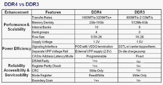
DDR4- Latest DRAM is Here

http://www.simmtester.com/page/news/showpubnews.asp?num=179
On May 2012 Micron announced DDR4 samples - First DDR4 DRAM from Micron


More about DDR4 at Why migrate to DDR4?
  • "Improved capacity and performance scalability: 
DDR4 is organized differently from DDR3—specifically in the area of how DDR4 is designed to support high-speed multi-core processors. The 8-Gb DDR4 SDRAM device with 4-bit-wide data bus interface (x4), for example, is internally organized as a device with four bank groups and four banks in each bank group...
  • Improved power efficiency:
Aside from further reducing the DRAM I/O voltage (VDDQ) from 1.35 V used by DDR3L DRAM devices to 1.2 V, the DDR4 SDRAM device also specifies that a separate VPP voltage supply be provided to support high DRAM core word line voltage requirements...
  • Improved reliability, availability and serviceability (RAS):

 DDR4 SDRAM specification improves RAS is that DDR4 device supports command and address parity error detection, as well as recovery from parity error...supports a connectivity test mode, so that a system controller can test and detect connectivity faults without needing to go through DRAM initialization sequencing...The DDR4 register also provides enhanced RAS over the DDR3 register in that the DDR4 register can be configured to support command blocking upon detection of a parity error.."


It will still be awhile before DDR4 will replace DDR3.

Ron
Insightful, timely, and accurate semiconductor consulting.
Semiconductor information and news at -
http://www.maltiel-consulting.com/


Kristin Lewotsky
10/17/2013 10:30 AM EDT