Friday, May 4, 2012

Apple's A5 Die Shrink, Improve Battery Life, Cut Cost

A teardown of a new iPad reveals a shrunk SoC die (see below). In second  half of 2011 an iPad's processor was made in the 45nm manufacturing process, while the current iPad seems to use a 32nm process.

The new 32nm A5 has a chip die area of only 69mm2 while in the 45nm process it was more than 120mm2 . I predicted that Apple will shift soon to 32nm process to improve battery life on March 22 in my blog post  New iPad-Teardown: Why Apple's A5X uses 45nm

This shrink will substantially reduce the cost of the A5 for Apple as Samsung improve the die yield of its  32nm high-k + metal gate LP manufacturing process.


Ron Maltiel


The iPad 2,4 Review: 32nm Brings Better Battery Life


by Anand Lal Shimpi on 5/4/2012 12:50:00 AM
http://www.anandtech.com/show/5789/the-ipad-24-review-32nm-a5-tested

When Apple launched the 3rd generation iPad (as the new iPad), it also dropped the price of the entry-level 16GB WiFi iPad 2 to $399. Apple's products tend to hold their values exceptionally well, so this two-tablet strategy made sense. Apple also proved the success of discount-the-previous-gen strategy with its iPhone line, where you can now buy current, n-1 and n-2 generations of iPhones at prices separated by $100.

What's different with the $399 iPad 2 is that Apple used it as a vehicle to introduce a new hardware platform, or more specifically, a new SoC.


When Apple launched the 3rd generation iPad (as the new iPad), it also dropped the price of the entry-level 16GB WiFi iPad 2 to $399. Apple's products tend to hold their values exceptionally well, so this two-tablet strategy made sense. Apple also proved the success of discount-the-previous-gen strategy with its iPhone line, where you can now buy current, n-1 and n-2 generations of iPhones at prices separated by $100.

What's different with the $399 iPad 2 is that Apple used it as a vehicle to introduce a new hardware platform, or more specifically, a new SoC.


The 32nm HK+MG Apple A5 SoC

Prior to the new iPad announcement there were three versions of the iPad 2:


iPad 2,1 iPad 2,2 iPad 2,3 iPad 2,4

A5 SoC 45nm LP 45nm LP 45nm LP 32nm LP

Connectivity WiFi WiFi + GSM WiFi + CDMA WiFi


Connectivity WiFi WiFi + GSM WiFi + CDMA WiFi
The 2,1 was WiFi-only, the 2,2 was GSM and the 2,3 was CDMA. The new addition to the family is the iPad 2,4. The 2,4 replaces the original iPad 2,1. It's also only available in a single capacity.


There's no known way to tell whether you're getting an iPad 2,4 vs. the older iPad 2,1 without opening the box. The 2,4 unit I ended up with was made in China, ruling out manufacturing region as a way of telling. The external box looks identical, as does the device itself.

The newer iPad 2,4 units should come with iOS 5.1 preloaded, while any older iPad 2,1 stock may have 5.0.1 or older. But the most accurate way to tell is by looking at what a utility like Geekbench will tell you about the hardware:

This particular iPad 2,4 sample came from Best Buy, and several attempts to find one elsewhere came up short. All indications seem to point to the iPad 2,4 being relatively rare, which makes sense considering what's inside it.
Although the iPad 2,1 and its 3G brethren all used a 45nm Apple A5 SoC, the iPad 2,4 uses a die-shrunk 32nm version. The performance remains the same, but the die is much smaller. This isn't however just a normal die shrink, as Apple is using Samsung's 32nm high-k + metal gate LP transistors for this new A5 die. Intel was first to make the HK+MG transition back at 45nm in 2007 and correctly predicted that no one else would make the move until 32nm at the earliest.

Transistors are amazingly complex to fully understand, but at a high level they're quite simple. Imagine a transistor as a silicon based switch. When on, current flows, and when off, current stops flowing. The smaller you make a transistor, the more likely it is to misbehave. If current flows while the transistor is off, you waste power. This is known as leakage current and can come from a number of sources.


One such source is the gate oxide/gate dielectric, a particularly thin part of modern day transistors - on the order of a handful of atoms thick. Thinning the gate dielectric is desirable up to a certain point, after which the dielectric simply leaks too much power. Switching to a different material here, specifically one with a higher dielectric constant (a higher k-value), can significantly reduce leakage current and mitigate this issue. This is exactly what the first part of Samsung's 32nm high-k + metal gate process does.

The second half of the new process is the introduction of a metal gate electrode. Switching from a polysilicon to a metal gate electrode results in higher drive current by elimination of a region of depleted conducting carriers between the gate electrode and gate dielectric.


The combination of these two innovations results in less wasted current and more efficient current delivery, which in turn can give us a more power efficient chip. It's a net win. It makes manufacturing more complex, and there's definitely a learning curve to implementing it, but after you get over that hurdle it becomes just another part of the process.

The More Cost Effective Die

Traditionally the move to a smaller process node brings about an increase in transistor density. As transistors get smaller, you can fit more of them into the same space (or the same number into a smaller space). It's this basic principle that makes Moore's Law work. If you can keep shrinking transistor size by about 50% every two years, you'll theoretically be able to double transistor count at the same cost every two years (or cut cost in half every two years). In practice it doesn't work this well. Newer processes are always more expensive than their predecessors initially and logic scaling is never perfect.

It's rare these days that we actually see a pure die shrink anymore. With Intel's tick-tock model we almost always see increases in functionality to accompany each process node shift. In the case of Ivy Bridge, we actually saw a significant increase in transistor count thanks to an improved GPU. With Apple's 32nm A5 however, we truly end up with a die shrunk version of the 45nm A5 SoC. About the only part of the computing world where we see these pure shrinks is in the console space where performance doesn't have to go up within a generation, but cost must go down.


45nm A5 (left) vs. 32nm A5 (right)
45nm A5 (left) vs. 32nm A5 (right) - Source: Chipworks


 The original 45nm A5's die measured approximately 122mm^2. The new 32nm A5 has a surface area of only 69mm^2. That's actually amazingly good scaling at 57% of the old die size, as perfect scaling from 45nm to 32nm would be around 50.5%.


Die size comparison

Assuming Apple could make full use of a 300mm wafer (which it can't, wafers are round, chips are rectangular at best so there are some unusable chips), Samsung could deliver 579 45nm A5 die to Apple. The move to 32nm would give Apple 75% more die per wafer at 1015 chips. Again both of these numbers are over estimates as they assume full usage of the surface area of a wafer as well as 100% yields, but you can see the benefit of a smaller die. As long as wafer costs increase by a factor less than the 75% increase in number of die per wafer, Apple can effectively reduce SoC cost by going this route.

These ARM based SoCs are already fairly cheap - all selling well below $30 (many around $15) - so there's not a whole lot of cost savings here. On a product like the $399 iPad 2, where Apple needs to do its best to maintain margins while holding onto (and growing) market share, every last dollar matters.
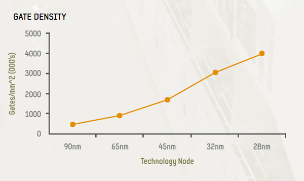


Gate density vs. process node at Samsung

There's another motivation for Apple however. Just as with any good microprocessor company, its best to introduce a new process technology on a known architecture. It's also a good idea to introduce a new process technology on lower volume products. The combination of both of these minimize risk. Should there be something wrong with the new process, introducing a new architecture on it just means you now have two very complex things to debug - the process technology and the chip's architecture. Should the new process not yield very well initially, you'd be similarly screwed if you were depending on it for your highest volume parts.
32nm A5 in iPad 2,4 (Source: Chipworks)


Apple decided to try out Samsung's 32nm HK+MG process on the A5 used in the 3rd generation Apple TV and some of the new iPad 2s. The former is a relatively low volume product for Apple, while the latter still moves in significant quantities. To deal with that fact, Apple is continuing to ship the original 45nm iPad 2,1 alongside the new 32nm iPad 2,4. Any hiccups in Samsung's production of the A5 and there are still more than enough iPad 2,1s to go around. The risk of moving to 32nm is effectively mitigated, while the learnings Apple gains from building the 32nm A5 will pay off later this year as Apple ramps up production of a 32nm SoC for use in the next iPhone. It's a very smart strategy, one you would expect from an experienced chip company - not a device vendor. When you consider that Apple employs chip architects who have worked on everything from the Athlon 64 to the Cortex A15, Apple's behavior is no longer that surprising.


Apple gets two benefits from the iPad 2,4: lower manufacturing costs, and experience with Samsung's 32nm HK+MG process which it will later use in much greater volumes. What about customers who end up with an iPad 2,4? Better battery life and cooler operation, of course.


Impact of HK+MG at Samsung


Remember the basics of Samsung's 32nm HK+MG process: a 40% performance improvement at the same leakage, or a 10x reduction in leakage at the same switching speed. As the iPad 2,4 retains the same clocks as the initial iPad 2, the benefit realized is a significant reduction in leakage current. This translates to tangibly better battery life.


Significant Battery Life Improvements details at http://www.anandtech.com/show/5789/the-ipad-24-review-32nm-a5-tested/2
.....

Final Words

If Apple's A5 is any indication, Samsung's 32nm HK+MG process is extremely capable. Assuming Apple didn't change any fundamentals of its microarchitecture, the iPad 2,4's gains in battery life can be attributed directly to the process. The gains themselves are significant. We measured a 15% increase in our web browsing battery life, a nearly 30% increase in gaming battery life and an 18% increase in video playback battery life. Although Apple hasn't revised its battery life specs, the iPad 2,4 definitely lasts longer on a single charge than the original iPad 2.


If you're in the market for an iPad 2, the 2,4 is clearly the one to get - if you can find one that is. Unfortunately there's no sure fire way to tell that you're getting a 2,4 without opening the box and turning on the tablet, and I suspect most stores will get a bit irate if you're constantly buying and returning iPad 2s in search for a 32nm model. Presumably over time more of the available inventory will shift to 2,4 models, but based on our experiences in trying to find a 2,4 it's still pretty tough.


I would like to applaud Apple's 32nm migration plan. By starting with lower volume products and even then, only on a portion of the iPad 2s available on the market, Apple maintains a low profile and gets great experience with Samsung's 32nm HK+MG process. It's very clear that this is all in preparation for the next iPhone, which will almost certainly use Samsung's 32nm process and require it in significant volumes. It's obvious that Apple employs some very smart chip heads in Cupertino.


What I'd really like to see is a 32nm version of the A5X used in the new iPad. I don't know that there's much reason for that this year, especially when the 4th generation iPad will likely ship in the first half of 2013 with yet another new SoC (dual-core A15 + Rogue anyone?), but it'd still be nice to have. The power efficiency improvements are substantial and the 3rd gen iPad could definitely use them. Those of you who are waiting for the next iPhone should also be pretty happy about these results. Apple could easily deliver a higher clocked version of the A5 for the next iPhone while keeping power consumption equal to if not lower than where it's at today. The move to 32nm is going to be good all around it seems, and Samsung appears to be a very capable foundry partner for Apple. Despite all of the rumors of a rift in the relationship, the foundry side of things is working out well.

Micron Technology Likely Winner, Buying Chipmaker Elpida Memory

"Micron likely winner in bidding for Japan's Elpida-NHK" as predicted with details by Businessweek in Feb. 27, 2012 (see below)


Ron Maltiel


Micron Biggest Winner as Elpida Bankruptcy Sidelines Rival Tech

http://www.bloomberg.com/news/2012-02-28/micron-biggest-winner-as-elpida-bankruptcy-sidelines-rival-tech.html


Micron Technology Inc. (MU) will probably emerge as the top winner from the bankruptcy ofElpida Memory Inc. (6665), whose filing yesterday sidelines the last Japanese maker of computer memory chips and gives rivals the chance to scoop up factories on the cheap.
Elpida filed for Japan’s biggest bankruptcy in two years after chip prices plunged and it failed to win a second government bailout. The elimination of a top maker of dynamic random access memory would give the rest of the industry more control over production, helping to ease the price swings that have left Micron unprofitable for six of the past 10 years.
The headquarters building of Micron Technology Inc. in Boise, Idaho. Micron shares jumped 7.7 percent yesterday amid speculation that the company, the fourth-largest DRAM maker, might seek to acquire some of Elpida’s plants. Photographer: Matthew Staver/Bloomberg
Elpida Memory Inc. memory chips are displayed in this arranged photograph in Tokyo, Japan. Photographer: Tomohiro Ohsumi/Bloomberg

Elpida’s creditors will look for ways to recoup losses through the sale of such assets as a plant in Hiroshima valued at $1 billion by Sanford C. Bernstein & Co. For potential buyers such as Micron, that price tag would be about a fifth of the cost of building a new equivalent facility. That would fit with Micron’s strategy of trying tobuy up capacity cheaply, rather than making acquisitions that outstrip the company’s $1.9 billion in cash and compel it to take on debt.

“Micron is clearly the winner,” said Dan Berenbaum, a New York-based analyst at MKM Partners LP. “Now it’s a question of how much does Micron pay for the assets.”

Micron shares jumped 7.7 percent yesterday amid speculation that the company, the fourth-largest DRAM maker, might seek to acquire some of Elpida’s plants. Dan Francisco, a spokesman for Boise, Idaho-based Micron, declined to comment.

Elpida has facilities that are responsible for about 18 percent of DRAM industry output, making it the No. 3 supplier. A push to take the plants offline or use them for other kinds of chips would help ease oversupply and stem industrywide losses.

Falling DemandThe computer-memory industry has been grappling with a decline in demand, brought on by a global consumer shift to smartphones and tablet computers, which need less memory and typically use a different type of chip.

Elpida’s troubles were exacerbated by DRAM prices falling below the cost of production. Industry sales last year dropped 26 percent to $29.2 billion, according to an estimate by Gartner Inc. That followed a 72 percent surge in 2010.

The Japanese chipmaker was the product of a 1999 merger between the memory businesses of NEC Corp. and Hitachi Ltd., which exited the industry.
‘Ten-Foot Pole’If Micron makes a bid for some DRAM facilities, Elpida’s creditors will get an offer that’s “tough to swallow,” because the U.S. company knows it’s not likely to face any competition, said Hans Mosesmann, an analyst at Raymond James & Associates Inc.

“Nobody else is going to touch DRAM with a ten-foot pole,” said Mosesmann, who has a “strong buy” rating on Micron shares. “Micron is very practical. They don’t want all of Elpida.”
Earlier this month, Micron’s management told Mosesmann and other analysts the company is monitoring events in Japan to see if there are opportunities. Executives declined to comment on whether Elpida is one of them and what the company might do.
“It just doesn’t feel like there’s going to be any fresh capital put into the DRAM business,” Micron President Mark Adams said in an interview on Feb. 9. “If we’re right, then the industry is mature enough that consolidation could make a lot of sense.”
Elpida has total debt of about $4 billion and has reported five straight quarters of losses. Micron, which has been making acquisitions and driving industry consolidation for more than 10 years, has about $1.95 billion of debt, approximately equal to its cash reserves. The company has a target range for its debt- to-capital ratio of 20 percent to 25 percent. Its current cash plus market capital of $8.4 billion give it a debt-to-capital ratio of about 18 percent, according to data compiled by Bloomberg.
Debt GuidelinesIf Micron stays within those guidelines -- giving it the latitude to borrow about another $500 million -- it’s not going to have enough leeway to buy its Japanese rival, said Daniel Amir, a San Francisco-based analyst at Lazard Capital Markets LLC.
“They probably won’t just buy out Elpida,” Amir said. “They are not willing to break the bank. It’s not like they’re going to spend $2 billion.”

Samsung Electronics Co., which dominates the memory-chip business and is the only consistently profitable company in the industry, has said it will concentrate on running its own business, making it an unlikely bidder for Elpida’s assets.
“Samsung is not going to come to their rescue,” said Raymond James’s Mosesmann.
Profit StruggleExcluding Samsung -- which is also the world’s second- largest maker of mobile phones and the biggest maker of liquid crystal displays -- DRAM makers have struggled to make money.
Matching supply with demand poses a constant challenge in the market for DRAM for personal computers, where plants take years to come online and can’t be shut down cheaply. With factories costing billions of dollars to build, companies such as Elpida have found themselves facing debts they have trouble repaying.
In six of the past 10 years, industry companies have spent more cash than their operations have generated. Even including Samsung, whose share price has more than tripled, memory makers as a group have lost 40 percent of their market value since October 2002.
If output from Elpida’s plants is slowed down or halted, all of its rivals will benefit as supply gets closer to demand and prices stabilize, according to Shawn Webster, an analyst at Macquarie Capital USA Inc.
“Any time a competitor is in distress, it’s a positive for everybody else,” said Webster. “If you pull supply offline, that could help everybody in the DRAM industry.

Micron CEOEarlier this month, Micron lost longtime Chief Executive Officer Steve Appleton, who died in a plane crash. Mosesmann and other analysts speculated that his death might slow any possible negotiations for industry consolidation, because Appleton had been the driving force behind previous transactions.

Micron, which got its start with an investment from local potato magnate J.R. Simplot, became one of the largest makers of computer memory when it bought the memory operations of Texas Instruments Inc. in 1998. Since then, it has acquired plants from Toshiba Corp., bought control of a Japanese joint venture, and formed partnerships with Taiwan’s Nanya Technology Corp. and Intel Corp. to secure access to more production.
In 2008, as Germany’s Qimonda AG headed for bankruptcy and sought investments, Micron bought out its interest in Inotera Memories Inc. (3474)Qimonda subsequently went out of business, and its chipmaking equipment was sold off.
Micron has also walked away from opportunities. In April 2002, it abandoned a transaction under which it would have acquired the memory operations of South Korea’s Hynix Semiconductor Inc., the second-largest DRAM maker, after the companies couldn’t agree on terms.
‘In No Rush’One way that Micron might consider a purchase of Elpida would be if it could get cheap financing for a transaction from Elpida’s creditors, which are facing the dilemma of knowing that restructuring the company’s debt wouldn’t be enough to make it competitive again, according to Betsy Van Hees, a San Francisco- based analyst at Wedbush Securities. Elpida needs more money to invest in making its production more efficient, she said.
When asked on Feb. 10 whether he would take Micron’s debt level above 25 percent of its capital to make an acquisition that would consolidate the industry, Chief Executive Officer Mark Durcan told analysts he was going to be “very careful about putting the company in a position where we’re not confident we can deal with any additional debt.”
Still, he would consider taking the debt ratio higher if there was a good enough opportunity, he said.

Thursday, May 3, 2012

TSMC To Makes Processer Chip For Apple? Not so Quickly

DigiTime below states “Taiwan Semiconductor Manufacturing Company's (TSMC) plans to ramp up 20nm production ahead of schedule…to entice Apple”. TSCM already is having trouble processing enough 28nm wafers for their current customers, why would Apple want to give TSCM orders for the next generation 20nm process?

In addition, if we look at how Apple’s is handling the current A5 processor manufacturing. They currently use the 45nm process (New iPad-Teardown: Why Apple's A5X uses 45 nm). It indicates that Apple intentionally does not want to push the envelope of a new process technology at the same time that they are bringing up a new processor circuit. They prefers to use a more mature process while the pushing the limits on circuit design.

It is more likely that TSMC is more aggressive in developing the fab and the 20nm process just to enhance their market position relative to other foundry vendors for their current customers. See Nvidia: TSMC 20nm Essentially Worthless.
Another prespective is at TSMC has a “good chance” of winning Apple’s chip biz in 2014
Ron Maltiel


TSMC eyeing advanced process chip orders from Apple
Cage Chao, Taipei; Jessie Shen, DIGITIMES [Wednesday 2 May 2012]

Taiwan Semiconductor Manufacturing Company's (TSMC) plans to ramp up 20nm production ahead of schedule have prompted industry sources to speculate that the foundry will be aggressively striving for CPU orders for future Apple devices.

The present 28nm shortage at TSMC makes it more unlikely that the foundry could attract orders from Apple, the sources claimed. TSMC currently is unable to provide sufficient capacity to its existing 28nm customers, the sources said.

With orders placed by Qualcomm, Nvidia, Broadcom, TI and AMD, TSMC meets less than 70% of 28nm chip demand at present, the sources pointed out. While having tight supply of 28nm capacity, TSMC now hopes an early investment in 20nm technology will help the foundry engage in collaboration with potential clients such as Apple in advance and ensure enough capacity to meet demand, the sources indicated.

The sources added TSMC stands a good chance of landing CPU orders from Apple in 2014.

With regards to the speculation, Digitimes Research analyst Nobunaga Chai commented that the fundamental issue will still be whether Apple would use a 28nm or 20nm process to build its next-generation processor, and choose TSMC as its contract manufacturer. If TSMC succeeds in grabbing CPU orders from Apple, the foundry's supply capability should not be a problem at all, Chai said.

Apple still uses 45nm to make its newest A5X, and has Samsung Electronics build the chips.

TSMC has revealed plans to invest about US$700 million in building a 20nm R&D line in 2012 – instead of its originally-planned 2013. Acknowledging that demand for 28nm manufacturing capacity from its mobile product IC customers has been higher than expected since the process ramp-up, the foundry finds it necessary to put its 20nm process into production ahead of schedule. Demand for 20nm will also first come from the mobile device sector, and order volumes are likely to be huge during the initial ramp-up stage – similar to the situation 28nm has, TSMC said at its recent investors meeting.

TSMC also indicated that the firm has accelerated its pace of 28nm capacity expansion. The foundry expects to have its supply of 28nm chips close to catching up with demand in the fourth quarter of 2012, and satisfy demand completely by the first quarter of 2013.


Tuesday, May 1, 2012

Q4'11 NAND Flash Ranking, Can We Trust the Numbers?

The result for 2011 Q4 worldwide flash market sales and growth rankings are not accurate. The tables don't includes SanDisk whose total sales in 2011 was $5.66 billion.

While it is true that not all SanDisk's $5.66B is in Branded NAND, a reasonable portion of the $5.66 billion is. More details about SanDisk's results from 2008 to 2011 are available at Is Apple Squeezing Suppliers, Or Is SanDisk Simply Missing Out?

US Fabs Losing Their Edge. Really?


It is true that "As chip plants get pricey, U.S. risks losing edge", as the article state.

However we should keep in mind that Apple has Samsung manufacture their A5 processor (that runs the iPad) at Samsung's Texas fab.  Apple manufactures in Texas due to the need for a close interaction between Apple's R&D and the Fab development and manufacturing groups. Such eco systems of technologies are a very important part of the development, production, and product supply chain.

The US still has some good manufacturing fabs. Intel is a good example. Intel has been extending its lead in manufacturing since the HKMG 45nm process.
 
As the article mentions, the future of US semiconductors will be strengthened by the industry's joint development of 450mm wafer manufacturing. It is important for the USA to maintain their current position.

Thursday, April 26, 2012

Intel: "Fabless model collapsing". Is it correct?


Intel’s top process technology exec says the foundry model is collapsing.  A good manufacturing process is only one of the factors that leads to success in product and circuit strategies. Intel had been leading in manufacturing with the HKMG process since the 45nm process.

However, they were not able to use their manufacturing clout to lead in new areas such as the mobile phone microprocessor market.

TSMC, GlobalFoundries, and UMC will have to work closer with the fabless companies sharing resources and cost to address these challenges.


Ron Maltiel

Friday, April 20, 2012

Qualcomm and Nvidia 28 nm Wafers? Shortage...

Last quarter results from Qualcomm show again the impact of Moore's law breaking down. As detailed below, Qualcomm growth this quarter was limited by the supply of 28 nm wafers. Nvidia has been complaining about similar type of issues in the last few months.

It all is really tied to the bigger issues of increasing cost of developing and producing new process technologies. This fact is reducing the number of leading edge fabs.

Fabless companies to ensure their supply will need to share more of the development costs in order to gain higher priorities.


More information on foundries, fabs, and wafer supply is available at Forecasting Wafer Demand: Technology Migration, Bottlenecks (Link includes a chart of wafer demand by IC product type (i.e. DRAM, NAND, NOR, MPU, PLD, etc))

Ron Maltiel