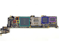
Detailed teardown with battery, NAND, A6, DRAM chips views at
http://www.ifixit.com/Teardown/iPhone-5-Teardown/10525/1
More on iPhone 5 Cost $199 BOM
Ron
http://www.maltiel.com/
http://www.ifixit.com/Teardown/iPhone-5-Teardown/10525/2
Step 15 
More chips on the underside of the logic board:
Qualcomm PM8018 RF power management IC
Hynix H2JTDG2MBR 128 Gb (16 GB) NAND flash
Apple 338S1131 dialog power management IC*
Apple 338S1117 Elpida memory MCP for LTE*
STMicroelectronics L3G4200D (AGD5/2235/G8SBI ) low-power three-axis gyroscope—same as seen in the iPhone 4S, iPad 2, and other leading smart phones
Murata 339S0171 Wi-Fi module
*Our buddies at Chipworks are making well-informed hypotheses here, and they're pretty good at what they do.
http://www.ifixit.com/Teardown/iPhone-5-Teardown/10525/3
Step 18 
Chips on a board. Kinda like ants on a log.
STMicroelectronics LIS331DLH (2233/DSH/GFGHA) ultra low-power, high performance, three-axis linear accelerometer
Texas Instruments 27C245I touch screen SoC
Broadcom BCM5976 touchscreen controller
Rather than a single touchscreen controller, Apple went with a multi-chip solution to handle the larger screen size, à la iPad.
Apple A6 Application processor
Qualcomm MDM9615M LTE modem
RTR8600 Multi-band/mode RF transceiver, the same one found in the Samsung Galaxy S III

-NAND-flash-Elpida-memory-MCP.jpg)

No comments:
Post a Comment