Monday, July 21, 2014

Bottlenecks: DRAM & Moore's Law

In addition to Moore's law slowing there are bottlenecks between the memory device and the CPU. 


The article below discusses
" How long will it will it take to find a technology so fundamentally different and better from anything we have today that we can do away with the DRAM latency and power consumption bottleneck?

There is a need for -
"A new RAM technology that cut main memory accesses by an order of magnitude would be reason enough to reevaluate the entire balance of resources on a microprocessor. If accessing main memory was as fast as accessing the CPUs cache, you might not need cache on the CPU die or package at all — or at least, you wouldn't need anything beyond L1 and maybe a small L2."

More about Moore's Law bottleneck from March 2012 Moore's Law End? (Next semiconductors gen. cost $10 billion)

Ron
Insightful, timely, and accurate semiconductor consulting.
Semiconductor information and news at - 
http://www.maltiel-consulting.com/


DRAM is pretty amazing stuff. The basic structure of the RAM we still use today was invented more than forty years ago and, just like its CPU cousin, it has continually benefited from the huge improvements that have been made in fabrication technology and density improvements. Less than ten years ago, 2GB of RAM was considered plenty for a typical desktop system — today, a high-end smartphone offers the same amount of memory but at a fifth of the power consumption.
After decades of scaling, however, modern DRAM is starting to hit a brick wall. Much in the same way that the CPU gigahertz race ran out of steam, the high latency and power consumption of DRAM is one of the most significant bottlenecks in modern computing. As supercomputers move towards exascale, there are serious doubts about whether DRAM is actually up to the task, or whether a whole new memory technology is required. Clearly there are some profound challenges ahead — and there’s disagreement about how to meet them.

What’s really wrong with DRAM?

A few days ago, Vice ran an article that actually does a pretty good job of talking about potential advances in the memory market, but includes a graph I think is fundamentally misleading. That’s not to sling mud at Vice — do a quick Google search, and you’ll find this picture has plenty of company:
DRAM scaling
The point of this image is ostensibly to demonstrate how DRAM performance has grown at a much slower rate than CPU performance, thereby creating an unbridgeable gap between the two system. The problem is, this graph no longer properly illustrates CPU performance or the relationship between it and memory.  Moore’s law has stopped functioning at anything like its historic level for CPUs or DRAM, and “memory performance” is simply too vague to accurately describe the problem.
The first thing to understand is that modern systems have vastly improved the bandwidth-per-core ratio compared to where we sat 14 years ago. In 2000, a fast P3 or Athlon system had a 64-bit memory bus connected to an off-die memory controller clocked at 133MHz. Peak bandwidth was 1.06GB/s while CPU clocks were hitting 1GHz. Today, a modern processor from AMD or Intel is clocked between 3-4GHz, while modern RAM is running at 1066MHz (2133MHz effective for DDR3) — or around 10GB/sec peak. Meanwhile we’ve long since started adding multiple memory channels, brought the memory controller on die, and clocked it at full CPU speed as well.
ddr_memory_data_rate
The problem isn’t memory bandwidth — it’s memory latency and memory power consumption. As we’ve previously discussed, DDR4 actually moves the dial backwards as far as the former is concerned, while improving the latter only modestly. It now looks as though the first generation of DDR4 will have some profoundly terrible latency characteristics; Micron is selling DDR4-2133 timed at 15-15-15-50. For comparison, DDR3-2133 can be bought at 11-11-11-27 — and that’s not even highest-end premium RAM. This latency hit means DDR4 won’t actually match DDR3′s performance for quite some time, as shown here:

This is where the original graph does have a point — latency has only improved modestly over the years, and we’ll be using DDR4-3200 before we get back to DDR3-1600 latencies. That’s an obvious issue — but it’s actually not the problem that’s holding exascale back. The problem for exascale is that DRAM power consumption is currently much too high for an exascale system.
The current goal is to build an exascale supercomputer within a 20MW power envelope,sometime between 2018 and 2020. Exascale describes a system that has exaflops of processing power, and perhaps hundreds of petabytes of RAM (current systems max out at around 30 petaflops and only a couple of petabytes of RAM. If today’s best DDR3 were used for the first exascale systems, the DRAM alone would consume 54MW of power. Clearly massive improvements are needed. So how do we find them?

Reinvent the wheel — or iterate like crazy

There are two ways to attack this problem, and they both have their proponents. One method is to keep building on the existing approaches that have given us DDR4 and the Hybrid Memory Cube. It’s reasonably likely that we can squeeze a great deal of additional improvement out of the basic DRAM structure by stacking dies, further optimizing trace layouts, using through-silicon vias (TSVs), and adapting 3D designs. According to a recent research paper, this could cut the RAM power consumption of a 100-petabyte supercomputer from 52MW (assuming standard DDR3-1333) to well below 10MW depending on the precise details of the technology.
While 100PB  is just one tenth of the way to exascale, reducing the RAM’s power consumption by an order of magnitude is unquestionably on the right track.
DRAM-Types
The other, more profound challenge, is the idea of finding a complete DRAM replacement. You may have noticed that while we cover new approaches and alternatives to conventional storage technologies, virtually all the proposed methods address the shortcomings of NAND storage — not DRAM. There’s a good reason for that — DRAM has survived more than 40 years precisely because it’s been very, very hard to beat.
The argument for reinventing the wheel is anchored in concepts like memristorsMRAM,FeRAM, and a host of other potential next-generation technologies. Some of them have the potential to replace DRAM altogether, while others, like phase change memory, would be used as a further buffer between DRAM and NAND. The big-picture fact that Vice does get right is that discovering a new memory technology that was faster and lower power than DRAM really would change the fundamental nature of computing — over time.
It’s easy to forget that the trends we’re talking about today have literally been true for decades. 11 years ago, computer scientist David Patterson presented a paper entitledLatency Lags Bandwidth, in which he measured the improvements in bandwidth against data accesses across CPUs, DRAM, LAN, and hard drives (SSDs weren’t a thing at that time). What he found is summarized below:
Latency lags bandwidth
In every case — and in a remarkably consistent fashion — latency improved by 20-30% in the same time that it took bandwidth to double. This problem is one we’ve been dealing with for decades — it’s been addressed via branch prediction, instruction sets, and ever-expanding caches. It’s been observed that we add one layer of cache roughly every 10 years, and we’re on track to keep that with Intel’s 128MB EDRAM cache on certain Haswell processors.
A new main memory with even half standard DRAM latency would give programmers an opportunity to revisit decades of assumptions about how microprocessors should be built. A new RAM technology that cut main memory accesses by an order of magnitude would be reason enough to reevaluate the entire balance of resources on a microprocessor. If accessing main memory was as fast as accessing the CPUs cache, you might not needcache on the CPU die or package at all — or at least, you wouldn’t need anything beyond L1 and maybe a small L2.
How long will it will it take to find a technology so fundamentally different and better from anything we have today that we can do away with the DRAM latency and power consumption bottleneck? Given how such a fundamental breakthrough would be vital to our ability to reach exascale computing and beyond, though, I hope it’s soon.

Thursday, July 17, 2014

DRAM as Non Volatile Memory =>Longer Battery Life

If your cell phone has non removable batteries, its DRAM memory can be treated as as a battery backed up nonvolatile DRAM. This improve battery life time and speed of mobile devices "data committed to flash was reduced by about 40 percent." See more in the article below. 

Actually, these benefits should be achieved in any mobile device with an improved operating system.

"several innovations.
·         Quasi-NVRAM. They set aside a portion of system DRAM to act as a battery backed up nonvolatile DRAM.
·         Device driver. A new device driver and library that manage I/O between the qNVRAM and system flash memory.
·         Persistent Page Cache. A new data structure in SQLite using quasi-NVRAM to perform in-place updates to the database files. 
·         Relaxed data flushing. Absorbs repeated writes to table files to further reduce I/O."


Ron
Insightful, timely, and accurate semiconductor consulting.
Semiconductor information and news at - 
http://www.maltiel-consulting.com/


Summary: You still hear complaints about nonremovable batteries in mobile devices – mostly Apple – but there is an upside: the ability to eliminate performance overhead. Here's how.
By Robin Harris for Storage Bits | July 14, 2014 in

Three researchers, Hao Luo, Lei Tian and Hong Jiang of the University of Nebraska, asked a simple and seemingly obvious question. Since our mobile devices have non-removable batteries why don't we treat DRAM as if it were nonvolatile?
Their paper, qNVRAM: quasi Non-Volatile RAM for Low Overhead PersistencyEnforcement in Smartphones was presented at the Usenix HotStorage conference last month.

Background
Typically Android mobile devices rely on SQLite, a shared preference key value store or the filesystem API to save persistent data on local flash. These employ journaling or file-level double-writes to ensure persistency.
The problem is that these techniques require multiple writes to storage, incurring substantial system overhead in devices that are already performance and power constrained.
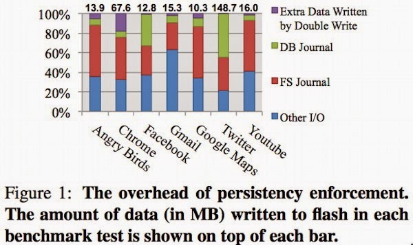
For example, they found that more than 75 percent of Twitter data was written for persistency reasons. Looking at a group of common mobile apps they found that anywhere from 37 percent to 78 percent of the data writes were for atomicity. From the paper:


Courtesy the authors.
Furthermore, it turns out that Android kernel reliability — where these data structures reside — is quite good, based on bug fixes and user support calls. They analyzed Android issue reports and found that only 10 reports or 0.05 percent of all 19,670 reported issues related to Android defects with unexpected or random power-off. That implies a small chance that unexpected power failure may occur.
The test
The researchers constructed a prototype test system with the with several innovations.
·         Quasi-NVRAM. They set aside a portion of system DRAM to act as a battery backed up nonvolatile DRAM.
·         Device driver. A new device driver and library that manage I/O between the qNVRAM and system flash memory.
·         Persistent Page Cache. A new data structure in SQLite using quasi-NVRAM to perform in-place updates to the database files. 
·         Relaxed data flushing. Absorbs repeated writes to table files to further reduce I/O.
Results
Implemented on an Android smartphone they found that
"...qNVRAM speeds up the insert, update and delete transactions by up to 16.33x, 15.86x and 15.76x respectively."

The Storage Bits take 
Furthermore, the amount of data committed to flash was reduced by about 40 percent. Given how common constant feed updates are on mobile devices, this is a significant result.
Some are miffed that many smartphones don't have easily removable batteries. This research shows the upside of such designs: all DRAM can be treated as NVRAM whether on Android or Apple's iOS.
Note that qNVRAM can't replace flash. DRAM is more power-hungry and costly than flash.
But research shows that by reducing the I/O overhead of the system with qNVRAM, significant gains in performance — and presumably battery life — can be achieved at very little cost. It also simplifies the problem of extending flash endurance.
It was obvious five years ago with the advent of non-removable batteries on phones and notebooks that engineers could take a new look at achieving persistency. Congratulations to the researchers for taking a rigorous approach to the problem.


Wednesday, July 9, 2014

Will NAND DIMMs take of?

Product like ULLtraDIMM (see article below) can take off  and become a major NAND SSD product line as SanDisk proves it in the market and Diablo Technologies license it to additional SSD suppliers.

More about ULLtraDIMM - Sandisk's future is far from ULLtraDIMM: Diablo tie-up holds promise Goldmine in the making for flash-DIMM server shop


This product is advancing memory system designs similar to the discussion in May 2012 blog - Apple NAND Storage in Upcoming MacBook Pros


Ron
Insightful, timely, and accurate semiconductor consulting.
Semiconductor information and news at - http://www.maltiel-consulting.com/


Will SanDisk Corp's New Product Revolutionize the Storage Industry?

In January, storage provider SanDisk  (NASDAQ: SNDK  ) announced ULLtraDIMM, a new form of flash storage that promises drastic speed increases for high-performance applications. SanDisk already has one big customer, IBM (NYSE: IBM  ) , for its ULLtraDIMMs, giving some early validation to this new technology. Let's take a closer look at ULLtraDIMMs and the effect they might have on the industry.

A bit of background
Storage, such as flash SSDs or hard disk drives, typically sits far away from the CPU and main memory. This means that there is latency due to the time it takes data to travel between the storage device and the CPU. For hard drives, this is not particularly relevant because their own internal latency is much greater than the transport latency. However, for flash, which is completely electronic and therefore much faster than hard disks, this becomes an issue.

The first approach to reducing this latency was to move flash from the drive and onto the PCIe communications bus, a step closer to the CPU. This provided an improvement, but it is not the optimal solution. PCIe still has latency compared to the memory bus, which sits right next to the CPU.

The new technology
Enter SanDisk's ULLtraDIMM, a flash storage that connects directly to the memory bus through the DIMM form factor, just like DRAM memory. Connecting to the memory bus gives ULLtraDIMMs a write latency of under 5 microseconds, compared to around 50 microseconds for PCIe SSDs. The shorter communication distance also means less power consumption, a crucial concern in densely packed enterprise servers.

Sandisk currently provides 200 GB and 400 GB ULLtraDIMMs, and users can add as many ULLtraDIMMs as they have memory slots. ULLtraDIMMs are implemented in a way that makes them look like a normal storage device to the operating system, but achieving this requires modifications to the BIOS which mean that ULLtraDIMMs are not yet plug-and-play devices.

Current and future applications
IBM has already signed up as a customer for Sandisk's ULLtraDIMMs. The enterprise giant has added some functionality to ULLtraDIMMs and rebranded them as eXFlash memory-channel storage. The new technology is available in IBM's X6 family of servers.

According to SanDisk and IBM, memory-channel storage will be useful for applications such as big data analytics, transactional databases, high-frequency trading, and virtualized environments. So far, it seems that IBM's X6 servers have been particularly popular with Wall Street firms. Speaking with EnterpriseTech, SanDisk senior director of marketing Brian Cox said, "we have all kinds of hedge funds begging us to deliver this."

What this means for the industry
It will take several more computer manufacturers to sign on in order to fully validate ULLtraDIMMs as a technology and to reveal the applications where it might best be used. SanDisk's management said that this will require evangelization and a surrounding ecosystem, and that they are continuing to invest in order to bring ULLtraDIMMs to wider adoption.  
Revenue from ULLtraDIMMs is estimated to be small in 2014. However, if ULLtraDIMMs catch on, competitors such as Micron  (NASDAQ: MU  ) (which is increasingly focusing on providing SSDs rather than selling chips as a commodity) will certainly follow with their own versions of memory bus flash. Currently, no other major flash provider is talking about this kind of technology; this means that SanDisk will have first-mover advantage for at least a few quarters.

It's also not clear yet to what extent memory-channel storage might displace PCIe or server-side flash. If the total cost of ownership for an ULLtraDIMM is comparable to or lower than current SSDs, the technology might eventually become the dominant form of flash storage. However, it is also possible that ULLtraDIMMs will complement rather than replace other forms of storage, much like flash itself did with hard disk drives in the enterprise space.

In conclusion
SanDisk has introduced a new form of flash storage called ULLtraDIMM, which sits right next to the CPU on the memory bus and provides much smaller latencies than existing solutions. In a partnership with IBM, ULLtraDIMMs have been shipping to enterprise customers, with expected applications such as high-frequency trading. While the technology certainly sounds promising and might be valuable for both SanDisk and IBM down the line, it's still too early to tell what effect this will have on the storage industry and enterprise computing in general. 
Warren Buffett: This new technology is a "real threat"At the recent Berkshire Hathaway annual meeting, Warren Buffett admitted this emerging technology is threatening his biggest cash-cow. While Buffett shakes in his billionaire-boots, only a few investors are embracing this new market which experts say will be worth over $2 trillion. Find out how you can cash in on this technology before the crowd catches on, by jumping onto one company that could get you the biggest piece of the action. Click here to access a FREE investor alert on the company we're calling the "brains behind" the technology.

Wednesday, June 18, 2014

eMMC/ eMCP - Samsung lose, Hynix gain $1.7Bil

The market of embedded flash controller grew from $6 to 9.5 Billion between 2012 to 2013 (see the article below). 

The article does not elaborate on the large increase of market share by Hynix and Toshiba. Hynix gain market share from 6.3% to 22.5% while Toshiba from 18.7% to 22.5%.

2013 Rank
Company
2012 Share
2013 Share
1
Samsung
56.6%
35.6%
2
Toshiba
18.7%
22.5%
3
SK Hynix
6.3%
22.5%
4
SanDisk
15.5%
14.0%

Wondering what is the cause for Hynix $1.68 Billion growth? It will be interesting to compare to the market share of the overall Flash NAND memory market shares. Is Apple behind Hynix growth?

Interesting to see today news that Quarterly Profits of Samsung Electronics Forecast to Drop
IT & Mobile Division, which accounted for over 60 percent of the electronics giant’s sales and business profits last year. The division’s smartphone and tablet PC shipments are estimated to have declined significantly in the current quarter. “According to our forecast, smartphone and tablet PC shipments have fallen at least 10 percent and approximately 20 percent from the preceding quarter, respectively,” said research analyst Song Myung-sup at HI Investment & Securities”


Ron
Insightful, timely, and accurate semiconductor consulting.
Semiconductor information and news at - http://www.maltiel-consulting.com/


Janine Love
6/16/2014 05:15 PM EDT 

Recently, Gartner released a report, "Market Share Analysis: eMMC and eMCP Vendors by Revenue, Worldwide, 2013." The top ranked vendor for eMMC and eMCP market was Samsung Electronics, with 35.6% of worldwide revenue (around $3.317 billion). The top four vendors, Samsung, Toshiba, SK Hynix, and SanDisk, claimed 95.4% revenue share in 2013, up from 90% the previous year. Sales of eMCPs saw higher growth in 2013 than eMMCs. In the report, Gartner attributes this to the increased support of eMCPs by application vendors for low-cost smartphones.


Table: Vendor revenue for eMMCs and eMCPs, worldwide, 2012-2013 (millions of dollars).

Officially known as JESD84-B50: Embedded MultiMediaCard (e.MMC), Electrical Standard (5.0), eMMC memory is a JEDEC standard that is currently in version 5.0. As JEDEC defines it, eMMC is an embedded non-volatile memory system that includes flash memory as well as a flash memory controller. The aim of the standard is to simplify the application interface design and free up the host processor from some of the low-level flash memory management tasks. About two years ago, we saw the introduction of embedded multi-chip package (eMCP) memory, which is eMMC memory with an additional DRAM module, developed for low-cost smartphones in an effort to speed time to market.

Figure: Position of different mobile memory systems in relation to cost and speed.
(Source: Gartner)

Gartner's principal analyst, Brady Wang, compiled the report. He found it surprising that sales of eMCPs saw higher growth in 2013. He also noted that TLC (also known as 3-bits-per-cell) NAND solutions for both eMMC and eMCP will see high adoption in 2014, both in smartphones and tablets. This will address the market demands for high levels of storage space while lowering costs.
eMMC and eMCP memory includes controllers. Some vendors are using their in-house controllers to gain a competitive advantage. 

Wang says: Some NAND flash vendors, including SNKD, Toshiba and Samsung, still use in-house controllers. Since the geometry of NAND flash moves fast and also the configurations of NAND flash chips between vendors are slightly different, it's important to have a close relationship between controller vendors and chip vendors. That's one advantage of in-house controllers. The other advantage is the cost.

Despite the success stories, challenges remain for mobile memory, and Wang identifies speed and performance as the top ones, as mobile memory is challenged to meet the demands of high-performance processors. As a result, he expects universal flash storage (UFS) memory to see its initial adoption in the second half of 2014, but only in very high-end, flagship products to start.
The advantages of UFS memory (as compared to eMMC/eMCP memory) are better performance, higher capacity, better bandwidth, better IOPS, and optimized performance for multithreaded applications, according to Wang. UFS uses a serial interface (eMMC is a parallel interface) and asynchronous I/O (eMMC is synchronous I/O), enabling it to efficiently move data between the host processor and mass storage.

Wang notes that currently the cost and power consumption of UFS is higher than eMMC, so this will constrain its adoption. However, with the introduction of multi-core architectures that require high-performance memory, UFS is well positioned. “Although the power consumption of UFS is higher than eMMC, its energy efficiency is better,” says Wang. He expects to see UFS in high-end smartphones, tablets, and ultrabooks. eMMC will still be the best choice for mid-to-low cost mobile applications. Wang also points to SATA SSDs as competition for UFS in ultrabook applications. Finally, he notes that UFS is not backward compatible with eMMC, which will slow its adoption in applications where eMMC is already used.


Monday, June 16, 2014

SSD Market Share/ SanDisk buys Fusion-io

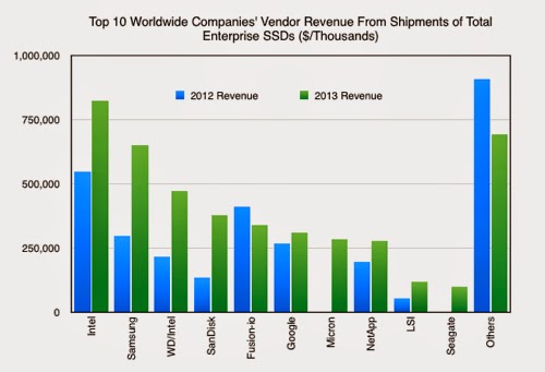
A recent survey by Gartner (see below) shows Intel and Samsung leading in shipment of SSD storage for enterprise.


Ron
Insightful, timely, and accurate semiconductor consulting.
Semiconductor information and news at - http://www.maltiel-consulting.com/


 IBM officially biggest all-flash array shipper - analyst

Gartner AFA data hits the street
By Chris Mellor13 Jun 2014 

No, it isn’t the greatly anticipated all-flash array magic quadrant, but it's great Gartner analysis nonetheless. The number-crunchers at Gartner HWQ have produced a Market Share Analysis: SSDs and Solid-State Arrays, Worldwide, 2013. Yummy. Let’s see what’s inside.
The doc, available as a download from Pure Storage (guess who's done well in the analysis) after registering a few details. It looks at both SSDs and all-flash arrays, which Gartner calls Solid State Arrays (SSAs) and IBM comes out as the leading SSA shipper – with Pure Storage second.
SSAs are defined carefully: ”SSAs are scalable, dedicated, solutions based solely on solid-state semiconductor technology for data storage that cannot be configured with HDD technology at any time. As distinct from SSD-only racks within ECB storage arrays, an SSA must be a stand-alone product denoted with a specific name and model number, which typically (but not always) includes an operating system and data management software optimised for solid-state technology.”
To cut a long story short, Dell and HDS all-flash array products are excluded, as are all-flash versions of – for example – EMC VMAX and VNX, and NetApp FAS arrays.
The SSD category embraces PCIe flash cards and also includes “self-contained solid-state NAND dual in-line memory modules (DIMMs), which must be used in dedicated slots in servers. Mainstream PC SSDs being used in servers are counted in this category due to end consumption.”
We’ll graph the information here, and you can read the detailed numbers by downloading the doc. The SSD info starts with worldwide vendor revenues:
Click chart for larger version
Total SSD revenues in 2012 were $7.2 billion, and in 2013 had risen to $10.99 billion, a 53.1 per cent increase.
Samsung as top dog got most of that with Intel, growing less, at number 2. Look at Sandisk’s rocketing growth up into the no 3 slot, closely followed by Micron. Toshiba held its fifth place but didn’t grow much. WD grew, Fusion-io declined and now we’re in the tail-enders.
Now let’s look at the enterprise SSD market:


Intel is top dog, not second-placed Samsung. WD, with its HGST/Intel SSDs is in third place followed by SanDisk successfully exhibiting its enterprise supplier credentials. Then there’s Fusion-io, which declined 2012 - 2013, Google with its internal use - amazing - Micron is a, we think, in a disappointing sixth place, NetApp a, for it, strong seventh then LSI and Seagate. EMC does not appear at all.
Now for the SSA numbers.
Here are the vendor revenue market share numbers:

Click chart to make it larger.
And here the actual SSA revenues by vendor:

Click chart to make it larger
IBM has had a wildly successful 2013 year, solidly overtaking Violin Memory to claim a dominating number 1 slot. Pure Storage has rocketed to the number 2 position in 2013 while Violin Memory slumped from first place in 2013 to third in 2013, illustrating the new management team’s uphill task. EMC has sprung into fourth place from a standing start and NetApp is not far behind in the fifth slot. Then there’s Nimbus Data and tail-ender Cisco - a dismal showing for the networking behemoth in our view, with startup SolidFire very close behind.
The SSA market was sized by Gartner at $236.5m in 2012, and 182.1 per cent higher at $667.3m in 2013. IBM’s SSA revenues grew at 278.1 per cent, Pure's at a magnificent 642.3 per cent and no other vendor outpaced the market, meaning they lost share.
Now this is artificial, as EMC, Kaminario, SolidFire and HP had no presence in Gartner’s numbers in 2013, but we can assert that Violin Memory, NetApp, Nimbus and Cisco all lost share from 2012 to 2013. With EMC, Kaminario, SolidFire and HP now in the SAA market we might expect these losses to continue in 2014.
The Gartner analysis contains more data, segment metrics and so forth. It’s worth a download and read if you’re interested.
Main takeaway? Big Blue really is big in SSAs, Pure Storage is living up to its hype, and the SSA market is growing at a fast lick. NAND the story goes on


Wednesday, May 14, 2014

3D NAND Race is On

[Image Source: Nikkei Electronics
Since Samsung announced their development of 3D NAND on August 2013 Samsung 3D Stacked NAND Flash has Engineering Samples . The other flash manufacturers have been trying to catch up while transitioning from planar NAND to 3D NAND. See below SunDisk and Toshiba announcement of their transitions plans (more information at 3D NAND Transition: 15nm Process Technology Takes Shape ).

Some background about 3D NAND and at 3D NAND flash is coming .  Also there is an interesting discussion regarding 3D flash from 2009 between Samsung and Toshiba 3D Cells Make Terabit NAND Flash Possible .


Ron
Insightful, timely, and accurate semiconductor consulting.
Semiconductor information and news at - http://www.maltiel-consulting.com/


 NAND Flash War

Toshiba, Sandisk Partnership to Mount Serious Challenge to Samsung

14 MAY 2014
Many computer memory chipmakers worldwide are said to be working to enlarge plants that produce NAND flash memory chips.  
According to the San Kei Shimbun on May 12, Toshiba, the world’s second-largest NAND flash memory chipmaker, decided to make an investment in a 3D V-NAND flash memory production facility in partnership with US-based semiconductor company SanDisk. Both companies are going to equally share the cost of the investment and inject 700 billion yen (7.419 trillion won, US$6.843 billion) for three years at the Yokkaichi Operation plant, the company’s memory production facility in Mie prefecture, Japan. At first, they estimated the amount at 400 billion yen. However, it nearly doubled after the two firms agreed to invest in the construction of a new facility and the replacement of the existing one.  
An increase in investment can be interpreted as Toshiba’s willingness to not lag behind its rival companies like Samsung Electronics, SK Hynix, and Micron. Given that Samsung completed the construction of its 3D V-NAND production facility in Xian, China on May 9, competition between Korean and Japanese firms to dominate the next-gen semiconductor memory market is expected to heat up again. 
Samsung began to mass-produce 3D V-NAND flash memory chips in its plant in Xian. 3D V-NAND flash memory where 40nm-class NAND flash memory is stacked up in 24 layers are twice as fast and last 10 times longer than 20nm-class planar NAND flash memory. The world’s largest computer memory chipmaker is planning to dominate the market by developing 3D V-NAND flash memory chips in a 36-layer stack soon.   
SK Hynix, the world's fourth-largest manufacturer of computer memory chips, is focusing on investing in NAND flash memory. For example, the firm converted its Cheongju M12 Plant that produced both DRAM and NAND flash memory chips into a NAND flash line last year in order to restructure the company whose focus was on DRAM. The chip-maker plans to mass-produce 3D V-NAND at the end of this year. Micron, which is in the third spot, recently changed its DRAM factory in Singapore into a NAND flash plant. 
Unlike its rivals, Toshiba only manufacturers NAND flash memory. Therefore, if competitors outperform the Japanese firm in the global NAND flash memory market, it will be fatal. Industry analysts are saying that Toshiba's lawsuit filed in March against SK Hynix for technology leakage despite its patent cross-licensing deal with the Korean firm was aimed at checking the Korean chip-maker's influence.  
According to the findings of market research firm IHS Technology, sales of NAND flash memory worldwide is estimated at US$25.8 billion last year, and the market continues to grow rapidly. In 2013, Samsung was the world's number one seller of computer memory chips with a 34.7 market share, followed by Toshiba (a 32.2 market share).