Tuesday, July 30, 2013

Server Storage 85% Faster w/o PCI Express

Latest advance in flash storage by changing system architecture and how flash storage is integrated are discussed in the article below. The potential for changes in flash storage architecture was already discussed in May 2012

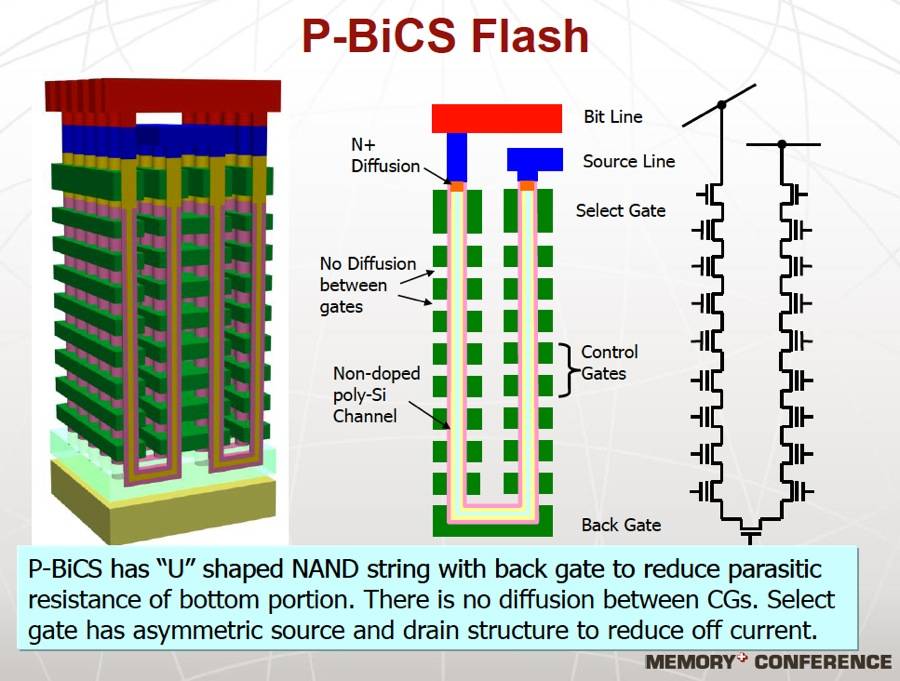
 "Diablo’s Memory Channel Storage (MCS) architecture, expected to show up in servers shipping later this year, allows flash storage components to plug into the super-fast channel now used to connect CPUs with memory. That will slash data-access delays even more than current flash caching products that use the PCI Express bus...

Diablo estimates that MCS can reduce latencies by more than 85 percent compared with PCI Express SSDs (solid-state disks)...

The connection is designed to be used by many DIMMs (dual in-line memory modules) in parallel, so each component doesn’t have to relinquish the bus for another one to use it. That saves time, as well as CPU cycles that would otherwise be used managing the bus"


Ron
Insightful, timely, and accurate semiconductor consulting.
Semiconductor information and news at - http://www.maltiel-consulting.com/


Flash breakthrough promises faster storage, terabytes of memory

In the ongoing quest for faster access to data, Diablo Technologies has taken what could be a significant next step.
Diablo’s Memory Channel Storage (MCS) architecture, expected to show up in servers shipping later this year, allows flash storage components to plug into the super-fast channel now used to connect CPUs with memory. That will slash data-access delays even more than current flash caching products that use the PCI Express bus, according to Kevin Wagner, Diablo’s vice president of marketing.
The speed gains could be dramatic, according to Diablo, helping to give applications such as databases, big data analytics and virtual desktops much faster access to the data they need most. Diablo estimates that MCS can reduce latencies by more than 85 percent compared with PCI Express SSDs (solid-state disks). Alternatively, the flash components could be used as memory, making it affordable to equip servers terabytes of memory, Wagner said.
Other than on-chip cache, the memory channel is the fastest route to a CPU, Wagner said. Not only do bits fly faster over this link, there are also no bottlenecks under heavy use. The connection is designed to be used by many DIMMs (dual in-line memory modules) in parallel, so each component doesn’t have to relinquish the bus for another one to use it. That saves time, as well as CPU cycles that would otherwise be used managing the bus, Wagner said.
The parallel design of the memory bus also lets system makers scale up the amount of flash in a server without worrying about diminishing returns, he said. A second MCS flash card will truly double performance, where an added PCIe SSD could not, Wagner said.
Diablo, which has been selling memory controllers for about 10 years, has figured out a way to use the standard DDR-3 interface and protocols to connect flash instead of RAM to a server’s CPU. Flash is far less expensive than RAM, but also more compact. The MCS components, which come in 200GB and 400GB sizes, will fit into standard DIMM slots that typically accommodate just 32GB or so of memory. The only adaptation manufacturers will need to make is adding a few lines of code to the BIOS, Wagner said.
Enterprises are more likely to use MCS as high-capacity memory than as low-latency storage, said analyst Jim Handy of Objective Analysis.
“Having more RAM is something that a lot of people are going to get very excited about,” Handy said. His user surveys show most IT departments automatically get as much RAM as they can for their servers, because memory is where they can get the fastest access to data, Handy said.
“Basically, you’d like everything to be in the RAM,” Handy said. Virtualized data centers, where many servers need to share a large set of data, need a shared store of data. But in other applications, especially with databases and online transaction processing, storage is just a cheaper and more plentiful—but slower—alternative to memory. “Everything that’s on the storage is there just because it can’t fit on the RAM,” he said.
To implement the MCS architecture, Diablo developed software and a custom ASIC (application-specific integrated circuit), which it will sell to component vendors and makers of servers and storage platforms. Flash vendor Smart Storage Systems, which earlier this month agreed to be acquired by SanDisk, will be among the companies using the MCS technology, Wagner said. In addition, a tier-one server vendor is preparing about a dozen server models with the technology and will probably ship the first of them this year, Walker said.
For the most part, Diablo doesn’t expect consumers or small enterprises to install MCS flash on their own computers. However, Diablo may work directly with enterprises that have very large data centers they want to accelerate, he said.
Using MCS flash to supplement DRAM would dramatically reduce the per-gigabyte cost of memory but also would allow for further consolidation of the servers in a data center, Wagner said. A large social networking company with 25,000 servers analyzed the MCS technology and said it would make it possible to do the same amount of work with just 5,000 servers.
That’s because the current DRAM-only servers can be equipped with just 144GB of memory, but MCS would allow each server to have 16GB of DRAM and 800GB of flash. With that much memory, each server can do more work so fewer are needed, Wagner said. Fewer servers would mean savings of space and energy, which would translate into lower costs, he said.

Thursday, July 25, 2013

Update: Chromcast Use Marvell and Azurewave


Google Chromcast is a game changer for tv media delivery. based on FCC documents (see below) "Marvell DE3005 chip, plus Azurewave hardware to handle its (2Ghz only) WiFi duties"


More in depth evaluation of Chromcast (power needs, iOS support, local files viewing)

Ron
Insightful, timely, and accurate semiconductor consulting.
Semiconductor information and news at - http://www.maltiel-consulting.com/


Even though Google only announced its new Chromecast HDMI dongle earlier today, we got our first peek at it in May. That's when the mysterious H2G2-42 leaked in FCC documents, with few details other than the name referencing Douglas Adams' book. As Anandtech's Brian Klug points out, the documents have been updated, and now include a few pictures of the Chromecast with its external casing removed. Inside there's a Marvell DE3005 chip, plus Azurewave hardware to handle its (2Ghz only) WiFi duties. Hit the link below to take a look, although at the $35 sticker price you can probably afford to do an iSuppli-style teardown of your own.

Wednesday, July 24, 2013

Smartphone: MediaTek Overtaking Qulacomm

The increasing importance of emerging markets to the smartphone market is helping MediaTek to gain on Qualcomm in term of shipment volume as is discussed in the article below.

More on MediaTek growth (from January 2013) with the help of "Coolpad, Huawei, Lenovo, Samsung and ZTE surged ahead of Apple.."


Ron
Insightful, timely, and accurate semiconductor consulting.
Semiconductor information and news at - http://www.maltiel-consulting.com/


Commentary: Qualcomm likely to be dethroned by MediaTek as the largest handset solution vendor

Cage Chao, Taipei; Steve Shen,  [Wednesday 24 July 2013]
 
With the planned release of LTE-enabled and 8-core SoCs in the fourth quarter of 2013, MediaTek will advance one-step further to beat venerable rival Qualcomm to become the world's largest supplier of smartphone solutions in terms of shipment volume.
 
Already taking up an over 50% of the solution market for the entry-level to mid-range smartphones in China and other emerging markets, the launch of LTE and 8-core CPUs will help ramp up MediaTek's share in the high-end smartphone solution market.
 
Additionally, the developments of application CPUs by Apple and Samsung Electronics, in-house for their high-end smartphones have worked to limit Qualcomm's growth potential in the high-end smartphone solution market as Apple and Samsung were previously the two major high-end smartphone solution clients for Qualcomm.
 
The outstanding performance-price ratio of MediaTeks' smartphone solutions combined with market proven records of China-based branded and white-box smartphone vendors to launch differentiated models by optimizing MediaTek solutions have enabled the Taiwan-based fabless IC house to push sales of its smartphone solutions to Sony Mobile Communications, LG Electronics and Motorola Mobility, and therefore further expanding its share in the global handset solution market.

Tuesday, July 23, 2013

SanDisk and 3D NAND


SanDisk is strongly pursuing 3D NAND  with Toshiba. 3D NAND is a very strong contender for future advances in NAND shrinking. See more below


Some background about 3D NAND and at
3D NAND flash is coming

 Ron
Insightful, timely, and accurate semiconductor consulting.
Semiconductor information and news at - http://www.maltiel-consulting.com/


SanDisk starts beating path to 3D NAND flash

Reckons product ready for market by 2015

Monday, July 15, 2013

Update: Samsung Fab. Apple A9 Processor?

It make sense for Apple to hedge it bets and use both TSMC and Samsung (see article below). It doesn't hurt that Samsung already spends 7 Billion dollars on next generation fab.

Update: GlobalFoundries Should Appeal to Apple. Not likely that Apple will get into chip making business. However all these rumors help apple negotiate with various potential partners.

Ron
Insightful, timely, and accurate semiconductor consulting.
Semiconductor information and news at - http://www.maltiel-consulting.com/


Apple Reportedly Signs Deal with Samsung for 14-nm A9 Chips Starting in 2015


The Korea Economic Daily reports that Apple and Samsung today officially signed an agreement that will see the two companies working together on future A-series chips for Apple's iOS devices, with the deal specifically covering A9 chips based on a 14-nanometer process node starting in 2015. The claim comes just weeks after Taiwan Semiconductor Manufacturing (TSMC) confirmed a deal with Apple to begin producing A-series chips in 2014.
Samsung Electronics had supplied the AP [application processor] to Apple since 2007 but lost the contract to supply 20 nano AP A8 chips to Apple to Taiwan's TSMC last year when it was engaged in patent disputes with Apple. Samsung Electronics developed state-of-the-art 14 nano models ahead of its rival TSMC, regaining the order from Apple.
A previous report about Apple's agreement with TSMC had indicated that it was a three-year deal covering not only Apple's future A8 chip but also A9/A9X chips. The Wall Street Journal's report had indicated that Samsung would remain Apple's primary supplier through next year as TSMC began ramping up its production. 

As a result, it is unclear whether today's deal will see both TSMC and Samsung producing A9 chips for Apple or if Apple has already shifted gears to return to Samsung as its primary supplier as part of its long-term roadmap. 

Apple has reportedly been seeking to reduce its reliance on Samsung as a component supplier as the two companies have become fierce rivals in both the mobile marketplace and in the courtroom. The two companies have, however, continued working together in several areas, particularly where Samsung's competitors in the component market are unable to match its technology, production capacity, or pricing. 

The shift to TSMC for production of the high-profile main chips for Apple's iOS devices had been viewed as breaking one of the most significant remaining ties between Apple and Samsung, but it appears that Samsung has been able to bring Apple back into the fold by leading the charge to 14-nm chips. With partnerships with both Samsung and TSMC, it appears that Apple should be well-positioned to take advantage of whichever company takes the lead in developing the latest technologies. 

Late last week, it was reported that Apple had bought into a fab, perhaps with an eventual goal of producing its own chips for its mobile devices, although any such move is almost certainly years away given the need to ramp up expertise and facilities for such production.

Friday, July 12, 2013

Samsung 3rd Foundry Ranking, Soon 2nd?

Samsung is growing its foundry sales and looking to make microprocessors for companies that do not have their own fab lines ( Amazon, Sony and Nvidia ). Considering Samsung advances in foundry business in 2012 it is likely that Samsung will surpass GlobalFoundries in 2013 and be 2nd largest semiconductor foundry.

"dedicated semiconductor foundry capacity reached 150 thousand 300mm wafers per month in Q4 2012"

More about Samsung foundry business below.


Ron
Insightful, timely, and accurate semiconductor consulting.
Semiconductor information and news at - http://www.maltiel-consulting.com/


Samsung Electronics’ semiconductor division is currently the world’s third largest contract maker of chips, mostly due to the fact that it produces vast amounts of different application processors for Apple as well as its own consumer electronics divisions. However, as Apple is looking at different manufacturers and Samsung wants further grows, the company is eyeing other customers.
“Samsung is eyeing Amazon, Sony and Nvidia as customers to offset the lost volume caused by the Apple’s decision to reduce purchases,” a source with knowledge of the matter revealed to the Korea Times.
At present, Samsung is negotiating on a high level with Sony Corp. and Nvidia Corp., presumably over making their chips for smartphones, game consoles, tablets and maybe even personal computers in the future.
Amazon, which has yet to develop its own application processors for its tablets, smartphones and possibly e-book reading devices, has also talked to Samsung, but without any significant outcome, presumably because Amazon’s chip development is at its early stages.
“Samsung is entering a new chapter in logic chips. It is looking for companies with processor design technology, but without manufacturing facilities,” said one industry observer.
 
Samsung has competitive process technologies and vast production capacities to satisfy demands from even such huge clients as Apple. The South Korean company is among a few foundries in the world who has leading-edge manufacturing processes, including 32nm and 28nm, and which is on-track to start making logic chips using 20nm and 14nm in the coming year.
According to market tracker IC Insights, in 2012, Samsung almost doubled its foundry sales and surpassed UMC to become the third-largest IC foundry in the world, according to estimates by IC Insights market tracking firm. It is believed that the company’s dedicated semiconductor foundry capacity reached 150 thousand 300mm wafers per month in Q4 2012. Using an average-revenue-per-wafer figure of $3000, Samsung’s IC foundry capacity currently has the potential to produce annual sales of about $5.4 billion.

Wednesday, July 10, 2013

Latest Transistor Channel (Moore Law Getting Too Expensive)


Moore law is getting too expensive to maintain the scaling march toward smaller devices. There are efforts to change the transistor channel as discussed below.
 
Some background on Fin-FET.
 
 
Ron
Insightful, timely, and accurate semiconductor consulting.
Semiconductor information and news at - http://www.maltiel-consulting.com/


Changing the Transistor Channel

Ending silicon’s central role in transistors could maintain the march of Moore’s Law

 
Illustration: Harry Campbell
The transistor isn’t shrinking the way it used to. The best ones we have today are a patchwork of fixes and kludges: speed-boosting materials that push or pull on the silicon center, exotic insulators added to stanch leaks, and a new geometry that pops things out of the plane of the chip and into the third dimension. Now, to keep Moore’s Law going, chipmakers are eyeing another monumental change in transistor architecture.
This time, they’re taking aim at the current-carrying channels at the very heart of the device, replacing the silicon there with germanium and compound semiconductors known as III-Vs. If all goes well, these materials could usher in a new generation of speedier, less power-hungry transistors, allowing for denser, faster, cooler-running chips.
But for alternate transistor channels to be accepted, engineers must find a way to build them on industry-standard silicon wafers. That’s no small feat. The atoms in the alternative semiconductors are spaced farther apart than in silicon, making the crystals difficult to grow without creating device-killing defects.
Still, industry experts say, it is quite possible that silicon fabs will ramp up production of these transistors as early as 2017. One promising approach, under development in Belgium, saves on materials and minimizes defects by precisely depositing the new materials into nanometer-scale trenches etched into standard silicon wafers. The resulting chips could trim energy consumption at data centers, boost the battery life of mobile devices, and help keep Moore’s Law going well into the next decade.
Modern transistors are built into silicon wafers through the addition of trace amounts of other materials, called dopants. Dopant atoms alter the electronic properties of the material in order to form the three core parts of the transistor: the source and drain regions, which spit out and receive charge carriers, and the current-carrying channel, which runs between them. More at  Transistor Channel Future
07transistorChannel

Friday, July 5, 2013

30% Faster Smartphone w/FinFET Atom (Intel)


Mysterious Android device with Intel's Bay Trail (FinFET Atom) chip establishes AnTuTu benchmark records (43,416 points)
Today, a mystery Android 4.2.2 device running Intel’s next generation of mobile processors – Bay Trail (FinFET Atom) – has surfaced, which blows those chart-topping numbers clean out of the water. The smartphone or tablet posted an unheard so far score of over 43,000 (43,416 points). This is apparently at 1.1GHz, while running Android 4.2.2 Jelly Bean. The first benchmarks of Intel’s upcoming Bay Trail SoC is around 30% faster than Qualcomm’s Snapdragon 800 clocked at 2.3GHz, the fastest ARM chip on the market. By comparison, the latest Galaxy S4 with LTE-Advanced support, with the Snapdragon 800, scores 31,491. To round out the comparison, Exynos 5 Octa (in the Galaxy S4) scores around 26,275, and Snapdragon 600 scores around 24,716. Bay Trail-T is Intel’s upcoming 22nm tablet-oriented SoC with four Silvermont cores, due out sometime this year (probably fall).

How good would the battery life be?


Ron
Insightful, timely, and accurate semiconductor consulting.
Semiconductor information and news at - http://www.maltiel-consulting.com/

 Mystery device running on Intel’s Bay Trail thrashes competition

http://techivian.com/015-mystery-device-running-on-intels-baytrail-thrashes-competiton/

If you thought Snapdragon 800 is the summit at which mobile processing power is going to peak for at least 2013, wait until you read this. No it’s neither Tegra, nor Exynos that we’re talking about. Instead, the Snapdragon 800 might soon be dethroned by none other than an Intel Atom processor.
bay trail vs snapdragon
A mystery device codenamed byt_t_ffrd10 was spotted on popular benchmarking tool, AnTuTu. The device featured an Intel Bay Trail processor (that will be the successor to Clover Trail+) and was clocked at just 1.1GHz instead of its usual speed of 2.1GHz. Now this is where it gets exciting. The device managed to attain a score of 43416 on AnTuTu running on Android 4.2.2. To give a fair idea of how huge that number is, the recently launched Xperia ZU and Galaxy S4 LTE-A with Snapdragon 800 could only achieve close to 34,000 points in the benchmark test. Snapdragon 600 and Exynos 5 Octa fall even behind with close to 24,000 points and 26,000 points respectively.
bay trail antutu
Now the only concern remaining would be the power usage of Bay Trail processor. Of course if Intel could master that as well, we wouldn’t have to tell you what you can expect on Galaxy S5 or probably other flagships from LG and others.

Wednesday, July 3, 2013

Interconnect Issues: History and Future Prospects

Interconnection play a key role in shrinking semiconductor chips, the latest interconnection issues are discussed below:

"The research pipeline of the semiconductor industry involves increasingly radical potential solutions to carry technology advancement through dimensional scaling to beyond-conventional CMOS. Many logic devices are under investigation to extend Moore’s Law to beyond the year 2020. These logic devices differ in structure and operating principles, and include various physical quantities that may be used for encoding information, such as charge, electric dipole, magnetic dipole (spin), orbital state, mechanical position, light intensity, etc. However, any device technology that offers advantages in performance, power dissipation or ease in dimensional scaling will have to be complemented with an interconnect technology that offers similar trades to avoid major bottlenecks due to interconnects. Various carbon-based interconnects were shown to have comparable or better performance compared to Cu/low-k in terms of both resistance-capacitance (rc) product and energy-delay-product."
 
Ron
Insightful, timely, and accurate semiconductor consulting.
Semiconductor information and news at - http://www.maltiel-consulting.com/
 

See an earlier article below

Interconnect Issues: History and Future Prospects, Part 2

Ahmet Ceyhan, Azad NaeemiGeorgia Institute of Technology
The research pipeline of the semiconductor industry involves increasingly radical potential solutions to carry technology advancement through dimensional scaling to beyond-conventional CMOS. Many logic devices are under investigation to extend Moore's Law to beyond the year 2020. These logic devices differ in structure and operating principles, and include various physical quantities that may be used for encoding information, such as charge, electric dipole, magnetic dipole (spin), orbital state, mechanical position, light intensity, etc.[1] However, any device technology that offers advantages in performance, power dissipation or ease in dimensional scaling will have to be complemented with an interconnect technology that offers similar trades to avoid major bottlenecks due to interconnects, which were described in [2]. Various carbon-based interconnects were shown to have comparable or better performance compared to Cu/low-k in terms of both resistance-capacitance (rc) product and energy-delay-product (EDP).[2]
 
The aim of this article is to investigate the interactions of interconnects with various voltage-controlled, charge-based devices similar to the conventional Si-CMOS transistor, including high-performance and ultra-low-power options. For that purpose, we pair finFETs, MOSFET-like carbon nanotube FETs (CNFETs), homojunction III-V tunnel FETs (TFETs) and sub-threshold CMOS devices with conventional Cu/low-k and emerging interconnect options; and we compare the relative performances at the circuit level. These device and interconnect technology options are illustrated in Figure 1. Since various device technologies offer very different characteristics in terms of the output current, input capacitance, subthreshold swing, etc., the constraints that they put on interconnects and the best interconnect option for each device are different as well.
 
This difference stems from the fact that the impacts of technology parameters of various interconnect technologies on the speed and energy advantages of a circuit may differ depending on the transistors used. Emerging carbon nanotube (CNT) and graphene nanoribbon (GNR) interconnects are mostly more resistive than Cu/low-k [3,4], but they offer lower capacitances.
 
Based on the Berkeley Short-channel IGFET Common Gate Model (BSIM-CMG),[5] predictive technology models (PTMs) for finFET devices are developed jointly by the Arizona State University PTM Group and ARM.[6] The development of the model parameters for the BSIM-CMG model is performed using the scaling theory of multi-gate devices, physical models and ITRS projections. Compared to planar bulk CMOS devices, finFET devices have significantly improved short channel effects (SCE) due to better electrostatics, can carry more current and offer improved area efficiency. The channel width is quantized; hence, the number of fins has to be optimized for drive current choices.
 
CNFET devices are alternative solutions to performance enhancement of transistors in the "atomic dimension limit" beyond 2020. A compact model developed by Deng et al.[7] is calibrated to meet reasonable ON current requirements while controlling the threshold voltage to keep leakage current at a reasonable value; and used for simulating MOSFET-like CNFET gates at the 16 nm technology node to predict the circuit- and system-level properties of CNFET devices. This model includes various non-idealities, such as the quantum confinement effects on both circumferential and axial directions, elastic scattering in the channel region, the resistive source/drain, the Schottky-barrier resistance, the acoustical and phonon scattering in the channel region, the screening effect by the parallel CNTs in CNFETs that contain multiple parallel CNTs under the same gate, and parasitic gate capacitances. The rest of both articles
 
Interconnect