Monday, August 26, 2013

Longest Battery Life Smartphone: Moto X (Teardown)

Below are some snapshot from Ifixit teardown of Google/ Motorola new cell phone. One of the key features of Motorola cell phones have been their very long battery life. Is it due to the combination of Qualcomm processor and the power management chip, some of the other chips, or their custom system architecture (software/ hardware)?

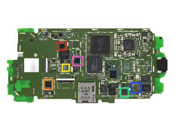
The key chips in Moto X are listed below.

Ron
Insightful, timely, and accurate semiconductor consulting.
Semiconductor information and news at -
http://www.maltiel-consulting.com/


Motorola Moto X Teardown

 
Image #1

Step 1 — Motorola Moto X Teardown 

  • The love child of Motorola and Google is here, and we are dying to crack open the little Motoroogle.
  • Technical Specifications:
    • Dual-core 1.7 GHz Qualcomm Snapdragon S4 Pro processor
    • 2 GB RAM
    • 4.7-inch 1280x720 pixels AMOLED display
    • 16 or 32 GB internal storage
    • Qualcomm Adreno 320 GPU
    • .........
    • Image #1

      Step 9 

      • Motorola claims the Moto X battery can power through an amazing 24 hours of "mixed usage."
      • How does the Moto X accomplish such a feat with a 3.8 volt, 2200 mAh Lithium ion battery? The secret is in the X8 Mobile Computing System.
      • The Motorola X8 Mobile Computing System is comprised of a Qualcomm Snapdragon S4Pro family processor, a natural language processor and a contextual computing processor.
      • Motorola developed a custom system architecture, which, when coupled with eight processor cores, allows for the delegation of processing power:
        • 4 graphics processor cores for "stunning clarity"
        • 2 application processor cores for "swift action"
        • 2 low-power cores—"awaiting your next command"
      Image #2

      Step 10 

      • Out comes the upper midframe panel, housing the speaker, headphone jack, more antennas, and pressure contacts.
        • Yay, pressure contacts! We like spring pressure contacts because they don't require any work to disconnect.
      • This is possibly the most modular headphone jack we've ever seen. It pops right out of the upper midframe panel, spring contacts and all.

      10 MP rear-facing camera

    • Image #1

      Step 15 

      • Notable ICs on the motherboard:
        • Toshiba THGBMAG7A2JBAIR 16 GB eMMC NAND Flash
        • SK Hynix H9TKNNNBPDAR RAM (we assume that the Snapdragon S4 Pro is also layered under this IC)
        • Qualcomm PM8921 Power Management IC
        • Texas Instruments TMS320C55 Digital Signal Processor
        • NXP 44701 NFC Chip
        • Skyworks 77619-12 Multiband Multimode Power Amplifier Module for Quad-Band GSM / EDGE and Penta-Band (Bands I, II, IV, V, VIII) WCDMA/ HSDPA/ HSUPA/ HSPA+/ LTE
        • Texas Instruments MSP430 F5259 Mixed Signal Microcontroller
      Image #1

      Step 16 

      • Additional ICs:
        • Qualcomm WCD9310 Audio Codec
        • Qualcomm WCN3680 802.11ac Combo Wi-Fi/Bluetooth/FM
        • NXP TFA9890 High Efficiency Class-D Audio Amplifier
        • Skyworks 77737 SkyHi™ Power Amplifier Module for LTE Bands 12/17 (698-716 MHz)
        • EPCOS 7 959 Wireless LAN / Bluetooth Filters (IF)
        • 0V00660 A56G 1B

Wednesday, August 14, 2013

Samsung 3D Stacked NAND Flash has Engineering Samples

Yesterday Samsung announced 3D flash V-NAND at Flash Summit


A key advantage of 3D vertical scaling is that device and process development issues of silicon based technology are better understood than other future flash approaches that depends on integrating brand new materials. 

Two other strong flash vendors are also developing 3D Flash

Toshiba and Hynix

There is an interesting discussion regarding 3D flash from 2009 between Samsung and Toshiba
3D Cells Make Terabit NAND Flash Possible

Based on Samsung keynote announcement at the flash summit:

 1. Samsung is having already engineering sample now and it will be in production in 2014.

2. Unless there is some unexpected development, it sound like Samsung's 3D NAND (and similar flavors by its competitors) will be the mainstream future NAND technology.

3. A key issue which they did not explain is erase cycle. They only said that erase had to be optimized with specific circuits. 

4. Samsung has been developing it since 2003. Initially they just developed the CTF memory cell technology as a standard planar NAND (see my previous comments  and at http://maltiel-consulting.com/Samsung's_32-gigabit-Gbit_40-nm_CTF-NAND_uses_high-k.htm). However, that product was not a commercial sold.

6. The first 3D test product they made was 16G in 2011, the current one is 128Gb which is built using a stack of 24 layers.

7. Samsung is building it based on a standard known 30nm silicon technology, they said it is cost competitive (or cheaper?) than planar technology. I am not sure what are their assumptions are as far as cost, but they are probably correct that it will be cheaper than competing future technologies.


Ron
Insightful, timely, and accurate semiconductor consulting.
Semiconductor information and news at - http://www.maltiel-consulting.com/

Wednesday, August 7, 2013

Samsung’s 1Tb SSD: 3D Vertical NAND

The article below discuss using CTF instead of floating gate to create 3D flash memory with up to 1T SSD product next year.

" new V-NAND is manufactured at a 10nm process size, and it starts at a density of 128Gb per NAND chip. The NAND chips are constructed in layers, stacking up to 24 individual NAND cells on top of each other...

Samsung is claiming that at minimum, the CTF-based V-NAND has at least a 2x increase in lifespan over floating gate NAND, and perhaps as high as 10x. Additionally, write performance is doubled over floating gate NAND."

Already in 2006 Samsung discussed CTF memory cell for NAND chips CTF for 40nm 32Gb .

More on CTF in March 2012 (Micron/ Intel 20-nm 64G MLC NAND Flash Memory Reverse Engineered).

At MemCon on August 6, 2013 Samsung said that more details will be presented at Flash Summit next week.

Ron
Insightful, timely, and accurate semiconductor consulting.
Semiconductor information and news at - http://www.maltiel-consulting.com/


Samsung’s “3D Vertical” NAND crams a terabit on a single chip

Longer life, higher reliability, more performance—what's not to like?

SSD enthusiasts know all about SLC, MLC, and TLC, but there are some new acronyms in SSD town: V-NAND and CTF. Samsung announced in a press release last night that it has begun mass production of "3D Vertical NAND," a type of flash that it claims overcomes the existing limits on the design and production of existing NAND types. When we looked at those limits about a year ago, they seemed pretty significant; Samsung's V-NAND aims to neatly sidestep most of the issues.
Enlarge / Samsung's 3D Vertical NAND stacks up to 24 NAND elements on top of each other.


The new V-NAND is manufactured at a 10nm process size, and it starts at a density of 128Gb per NAND chip. The NAND chips are constructed in layers, stacking up to 24 individual NAND cells on top of each other. This lets S amsung scale the chip's capacity up without having to add more NAND cells in a series, or "planar scaling," as the traditional "just shrink 'em and add more cells" method is called.
The other acronym, CTF, stands for "Charge Trap Flash." Traditional NAND flash records zeros and ones by storing charge in a set of floating gate transistors, with the presence or absence of charge corresponding to a 0 or a 1 in single-level cell NAND, and the amount of charge corresponding to different multibit values in multi- and triple-level cell NAND (we have an extremely in-depth primer on the inner workings of SSDs if you want more details). However, Samsung's new V-NAND dispenses with floating gate transistors and uses a different method:
Samsung's CTF-based NAND flash architecture, an electric charge is temporarily placed in a holding chamber of the non-conductive layer of flash that is composed of silicon nitride (SiN), instead of using a floating gate to prevent interference between neighboring cells.
The longevity and reliability problems with standard floating gate transistor-based NAND have a lot to do with the large amounts of power required to perform erasures. Without taking too large a digression, each time a NAND transistor undergoes a program/erase cycle, it retains some additional electrons in its dielectric layer. Eventually, these trapped electrons alter the transistor's resistance to the point that it can no longer be reliably read. The problem grows worse as the NAND cell manufacturing process shrinks—smaller cells become useless at lower levels of retained charge.
Smaller NAND transistor gates means it takes a smaller retained charge to overwhelm the gates' ability to quickly and reliably change state.
Aurich Lawson

The switch from floating gate to Charge Trap Flash appears to negate a lot of these issues. Samsung is claiming that at minimum, the CTF-based V-NAND has at least a 2x increase in lifespan over floating gate NAND, and perhaps as high as 10x. Additionally, write performance is doubled over floating gate NAND.
Samsung predicts that V-NAND will scale up to 1Tb per individual NAND chip. Most SSDs use at least eight NAND chips in parallel, so V-NAND could lead directly to low dollar-per-GB 2.5-inch form factor SSDs of 1TB and beyond—capacities which many Ars commenters have said repeatedly that they desperately want. At that size, concerns over installing an operating system and a few games on a fast SSD and stashing non-speed-critical files on a larger HDD are moot, and most folks can simply use the SSD exclusively without worry. There's no word yet on exactly when a consumer-level SSD filled with V-NAND will become available, but Samsung's vertical integration likely means that the first V-NAND SSD will be a Samsung-branded product with a Samsung-branded SSD controller.