Moore law is getting too expensive to maintain the scaling march toward smaller devices. There are efforts to change the transistor channel as discussed below.
Some background on Fin-FET.
Ron
Insightful, timely, and accurate semiconductor consulting.
Semiconductor information and news at - http://www.maltiel-consulting.com/
Semiconductor information and news at - http://www.maltiel-consulting.com/
Changing the Transistor Channel
Ending silicon’s central role in transistors could maintain the march of Moore’s Law
By Richard Stevenson / 24 Jun 2013 | 20:50 GMT
Illustration: Harry Campbell
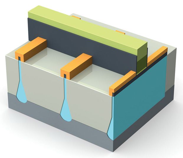
The transistor isn’t shrinking the way it used to. The best ones we have today are a patchwork of fixes and kludges: speed-boosting materials that push or pull on the silicon center, exotic insulators added to stanch leaks, and a new geometry that pops things out of the plane of the chip and into the third dimension. Now, to keep Moore’s Law going, chipmakers are eyeing another monumental change in transistor architecture.
This time, they’re taking aim at the current-carrying channels at the very heart of the device, replacing the silicon there with germanium and compound semiconductors known as III-Vs. If all goes well, these materials could usher in a new generation of speedier, less power-hungry transistors, allowing for denser, faster, cooler-running chips.
But for alternate transistor channels to be accepted, engineers must find a way to build them on industry-standard silicon wafers. That’s no small feat. The atoms in the alternative semiconductors are spaced farther apart than in silicon, making the crystals difficult to grow without creating device-killing defects.
Still, industry experts say, it is quite possible that silicon fabs will ramp up production of these transistors as early as 2017. One promising approach, under development in Belgium, saves on materials and minimizes defects by precisely depositing the new materials into nanometer-scale trenches etched into standard silicon wafers. The resulting chips could trim energy consumption at data centers, boost the battery life of mobile devices, and help keep Moore’s Law going well into the next decade.
Modern transistors are built into silicon wafers through the addition of trace amounts of other materials, called dopants. Dopant atoms alter the electronic properties of the material in order to form the three core parts of the transistor: the source and drain regions, which spit out and receive charge carriers, and the current-carrying channel, which runs between them. More at Transistor Channel Future
No comments:
Post a Comment