Thursday, September 27, 2012

iPhone A6 Teardown Update


iPhone A6 Polysilicon Layer
 Apple iPhone is still using Samsung's fab's 32nm HKMG process based on the chipwork teardown detailed below.

More on iPhone A6 Performance Improvement

Ron
http://www.maltiel-consulting.com/


http://www.chipworks.com/blog/recentteardowns/2012/09/21/apple-iphone-5-the-a6-application-processor/
Posted on September 21, 2012 by carav

Much has already been covered about the Apple A6 processor, whether it be the move to Apple-designed ARM cores or the possible fab transfer from Samsung to TSMC. Our job with these teardowns is to provide evidence-based information so as we complete work we will confirm what is possible (and for a reasonable cost – don’t expect the circuit schematics for the whole chip).
What we can say is that the foundry for the chip we have anlayzed is confirmed to be Samsung and that, from what we see this chip is a custom designed ARM core.

Lets look in more detail at the evidence.

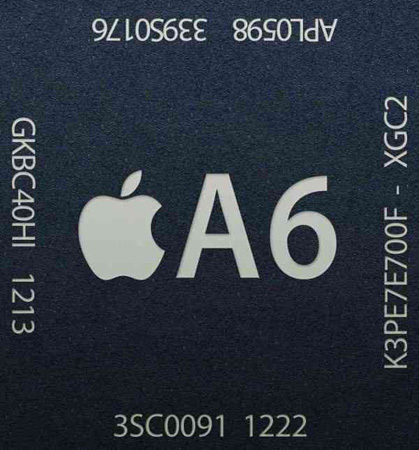
The die measures 9.70 mm x 9.97 mm and has the markings APL0589B01. The look of the markings is consistent with previous generation Samsung-fabricated parts.


Apple A6 Top Metal Die Photo (click to zoom)


Apple A6 Die Markings With a die area of 96.71 mm2 the die is considerably larger than the previous 2nd generation variant of the Apple A5 (~70 sq mm) which was fabricated by Samsung using their 32-nm HKMG process.


And finally (enough being coy), the following shots compare the Samsung 32 nm found in the A6 with the Samsung 32 nm in the A5 (2nd gen). We measure a contacted gate pitch of 130 nm to confirm this.

Apple A6 SEM Cross Section
Samsung 32 nm HKMG
Apple A6 - Samsung 32 nm HKMG
Samsung 32 nm HKMG from Apple A5
Apple A5 - Samsung 32 nm HKMG
Combining process generation with die size give you an idea of chip complexity. Simply put, if a die is larger at the same generation you can assume the chip is more complex, and in the case of the Apple A6 – this is certainly true. For comparison purposes, we are including some of the prior generation polysilicon die images to compare with the die size of this top metal image of the A6. Things will get really interesting when we can compare the block sizes of the A5 with the A6.
In order from left to right
A4 45 nm 7.3x7.3 mm
:


A5 45nm 10x12mm


A5 Gen 2
32nm 8.2x8.7 mm

A5x 45nm 12.9x12.8mm


A6 32nm 9.7x10mm
Let’s now turn our attention to the die layout. We see that there are three Power VR Graphics cores, as expected. Much of the world has been speculating on whether Apple is using an ‘out of the box’ ARM core or if they have custom designed some variant.


Apple A6 Polysilicon Die Photo (click to zoom)


Annotated Apple A6 Polysilicon Die Photo (click to zoom)


From the die layout we can see that the ARM core in the Apple A6 is about 50% larger than that previously found in the A5:


A5: 3.65 mm x 2.83 mm (10.3 mm2), each is 1.82 mm x 2.83 mm


A6: 4.15 mm x 3.81 mm (15.8 mm2), each is 4.15 mm x 1.91 mm


The feature that really jumps out at you in the A6 poly layer die photo is the dual ARM core. The layout for this CPU appears to have been done by hand. Normally large digital blocks of logic use automated “place and route” CAD software to layout all the digital cells and connect them. This is the style used on the rest of the digital blocks on this chip (shown below). This is also the style that has been used for the CPUs in all previous Apple iPhone and iPad processors. However, on this A6 chip, the ARM core appears to have been laid out by hand. This does lend credence to the current thinking that this is a custom ARM core specifically designed for the A6.


Typical automatically laid out standard cell block (A6 GPU)


Layout of the ARM core in the Apple A6

So this is the first Apple core we’ve seen done with custom digital layout. In fact, with the exception of Intel CPUs, it’s one of the first custom laid out digital cores we’ve seen in years! This must have taken a large team of layout engineers quite a long time. The obvious question is, why? This is a more expensive and time-consuming method of layout. However it usually results in a faster maximum clock rate, and sometimes results in higher density. Certainly one possibility is that Apple could not meet timing on a automatically laid out block, and chose to go with a custom laid out block. Was this a decision at the architecture stage, or did timing fail late in the design cycle and a SWAT team of layout engineers brought in to save the day? We’ll probably never know, but it is fascinating, and also 2X faster (according to the below image)


Apple promoting A6 performance at iPhone 5 launch


And now for a bit of the fun part


Last time around (with Apple A5X in the iPad 3) we gave out a full resolution die photo for people to use as their screen backgrounds. It seemed to be pretty popular so this time around, we’re doing it again. Given that the die is square and we are a bunch of engineers who don’t like to mess with reality, we didn’t get too creative with making it fit the 1136 x 640 screen.


However, we are also providing zoomed-in screen resolution versions of the rectangular graphics and logic cores for a better fit. Now you can show people your background and say, “my ARM core is fancier than your ARM core”.


Full die photo 640x649 (click to zoom and download)


Apple A6 Graphics Core (click to zoom and download)


Apple A6 ARM Cores (click to zoom and download)


__________________________________________


Other Pages in the analysis of the iPhone5


Page 1 – Initial Teardown of the iPhone 5


Page 2 – Camera and Battery


Page 3 – Apple A6 Analysis


Page 4 – A closer look at the RF Chips (coming soon)

Monday, September 24, 2012

NAND:Prices, Market Shares (Micron Up, Toshiba Down..)


NAND flash market share in July 2011
 Micron was able to increase its market share in NAND flash to 20.7%. based on IHS's report:

"Micron was able to claim some of the market share ceded by Toshiba. The Japanese maker in the second quarter saw its share decline by 9.5 percentage points sequentially, which occurred after strong growth in the first quarter....
Micron accounted for 80 percent of production from its joint venture with Intel, up from 62 percent in the first quarter. The increase was part of a revised capacity agreement between the two companies."


The pie chart shows how much Micron's market share improved since July 2011. (via https://www.semiconportal.com/en/archive/news/main-news/110715-toshiba-fab5-nand.html).


Since July 2011, NAND prices have been trending down. From the second article below:

"over the last two or so years, Micron, Samsung, SK Hynix and Toshiba began to expand their NAND production at a dramatic pace. The goal was to meet the anticipated demand for the next wave of product drivers, such as smartphones, solid-state drives (SSDs), tablets and ultrabooks.
Seeking to drive down product costs, particularly for SSDs, NAND vendors took the lead in process technology. For example, the Toshiba-SanDisk duo has been ramping up parts based on the world’s most advanced process, a 19nm technology.
The bottom fell out of the NAND market in recent times. NAND vendors built up too much fab capacity. Average selling prices (ASPs) for NAND fell by 46% in the first half of 2012. Demand for NAND in smartphones and tablets remains overwhelming, but SSD and ultrabook shipments have been disappointing thus far."


Ron
http://www.maltiel-consulting.com/


In a First, U.S.-Based Micron Takes 20 Percent Share of the NAND Flash Market

http://www.isuppli.com/Memory-and-Storage/News/Pages/In-a-First-US-Based-Micron-Takes-20-Percent-Share-of-the-NAND-Flash-Market.aspx
Dee Nguyen,     September 21, 2012

For the first time since it entered the industry seven years ago, U.S.-based Micron Technology Inc. managed to cross the 20 percent market share threshold in the NAND flash memory business during the second quarter.

Micron posted the strongest sequential performance of all NAND suppliers, with second-quarter revenue amounting to $897 million, up 6 percent from $846 million in the first quarter, according to an IHS iSuppli
In comparison, the other ranked suppliers all suffered revenue declines during the same period.

Despite overall NAND flash market revenue declining by 13 percent, Boise, Idaho-based Micron increased its market share to 20.7 percent in the second quarter, up from 17 percent in the first quarter, as presented in the table below.


“Defying weak demand and falling prices in the overall business, Micron expanded its NAND revenue and market share to reach the key 20 percent milestone for the first time since it started selling the memory in 2005,” said Dee Nguyen, memory analyst at IHS. “Micron not only successfully increased its bit shipments of NAND flash by a whopping 68 percent, it also benefitted from a reallocation in production from the NAND joint venture partner with Intel Corp., while capitalizing on the travails at its close competitor—No. 2-ranked Toshiba Corp.”

Intel and Toshiba Benefit Micron

See the rest at www.maltiel-consulting.com/nandprices-market-shares-micron-up.html


NAND Enters Tough Cycle

http://semimd.com/blog/2012/09/20/nand-enters-tough-cycle/
By Mark LaPedus

The NAND flash memory market is entering into a new and painful cycle, a period that will impact suppliers, OEMs and fab tool vendors alike.

For some time, there has been an oversupply and depressed pricing in the NAND market. In mid-2011, Micron, Samsung, SK Hynix and Toshiba put on the brakes in their capital spending plans. And in recent months, NAND suppliers in total have announced plans to cut 150,000 wafer starts per month, or about 12% of the world’s NAND capacity, amid ongoing losses and sluggish demand.

Just as suppliers moved to cut their production, spot shortages of NAND surfaced at some OEMs in early September. Most OEMs are not seeing any shortages, but that could all change. Apple, the world’s largest buyer of NAND, could cause some gyrations in the channels as it ramps up its new iPhone 5.

So what’s the outlook in the fluid and confusing NAND market? Amid a bitter legal battle with Samsung, speculation is rampant throughout the NAND industry about whether Apple will swap suppliers from Samsung to SK Hynix, Toshiba and Micron. If that happens, Samsung would face an oversupply in NAND, while others may see capacity shortfalls.

The outlook is also not so rosy for fab tool vendors, which counted on a big capital spending cycle for NAND. In fact, NAND suppliers are expected to push out their capital spending plans until June of 2013 and perhaps beyond, said Vijay Rakesh, an analyst with Sterne Agee.

The lack of capital spending is expected to create a shortfall in NAND capacity, creating perhaps a long cycle of acute shortages. Presently, there is a capacity glut for NAND. “Demand should catch up with capacity by mid-2013,” said Jim Handy, an analyst with Objective-Analysis. “Then, there could be NAND shortages from then until the middle of 2015.”

See the rest at www.maltiel-consulting.com/nandprices-market-shares-micron-up.html

Friday, September 21, 2012

iPhone A6 Performance Improvement

Using LPDDR2 DRAM memory with an A6 processor led to
"Roughly 33% more peak memory bandwidth than the iPhone 4S, which can definitely help feed the faster GPU and drive the higher resolution display"


More on Appple Teardown and on iPhone 5 Cost $199 BOM


   Ron
www.maltiel.com


iPhone 5 Memory Size and Speed Revealed: 1GB LPDDR2-1066


 http://www.anandtech.com/show/6297/iphone-5-memory-size-and-speed-revealed-1gb-lpddr21066
 by Anand Lal Shimpi & Brian Klug on 9/15/2012 8:53:00 PM


Quick analysis of the A6 SoC photos from the iPhone 5 launch event tells us all we need to know about the memory interface, speed and bandwidth of the new platform. As always, the A6 features a PoP stack combining the SoC itself and its DRAM. The package-stacked DRAM helps save space, which comes at a premium inside a device as small as a smartphone. PoP stacks are quite common in all modern smartphones.

Apple thankfully didn't obscure the details of its A6 slide at the launch event, which gave us a Samsung part number: K3PE7E700F-XGC2. Through crafty navigation of Samsung's product guide, Brian Klug got us the details. The K3P tells us we're looking at a dual-channel LPDDR2 package with 32-bit channels. The E7E7 gives us the density of each of the two DRAM die (512MB per die, 1GB total). The final two characters in the part number give us the cycle time/data rate, which in this case is 1066MHz.


Plug all of that into our memory bandwidth scaling chart and you get this:


Roughly 33% more peak memory bandwidth than the iPhone 4S, which can definitely help feed the faster GPU and drive the higher resolution display. Many vendors have been shipping LPDDR2-1066 so there's nothing too surprising here. There's understandably less bandwidth than in the 3rd gen iPad of course as the display/GPU requirements aren't nearly as high.

There's more than just memory clocks that will impact memory bandwidth here. It's unclear whether the A6 improves the memory controller Apple deployed in the A5. ARM architectures (especially in the A9 generation) have typically struggled getting good memory bandwidth efficiency. We'll have to see what happens with the A6.

iPhone Teardown Updated

Detailed teardown with battery, NAND, A6, DRAM chips views at
http://www.ifixit.com/Teardown/iPhone-5-Teardown/10525/1


More on iPhone 5 Cost $199 BOM


Ron
http://www.maltiel.com/


http://www.ifixit.com/Teardown/iPhone-5-Teardown/10525/2
Step 15 


More chips on the underside of the logic board:


Qualcomm PM8018 RF power management IC

Hynix H2JTDG2MBR 128 Gb (16 GB) NAND flash

Apple 338S1131 dialog power management IC*

Apple 338S1117 Elpida memory MCP for LTE*

STMicroelectronics L3G4200D (AGD5/2235/G8SBI ) low-power three-axis gyroscope—same as seen in the iPhone 4S, iPad 2, and other leading smart phones

Murata 339S0171 Wi-Fi module

*Our buddies at Chipworks are making well-informed hypotheses here, and they're pretty good at what they do.

http://www.ifixit.com/Teardown/iPhone-5-Teardown/10525/3
Step 18 


Chips on a board. Kinda like ants on a log.


STMicroelectronics LIS331DLH (2233/DSH/GFGHA) ultra low-power, high performance, three-axis linear accelerometer
Texas Instruments 27C245I touch screen SoC

Broadcom BCM5976 touchscreen controller

Rather than a single touchscreen controller, Apple went with a multi-chip solution to handle the larger screen size, à la iPad.
Apple A6 Application processor
Qualcomm MDM9615M LTE modem
RTR8600 Multi-band/mode RF transceiver, the same one found in the Samsung Galaxy S III

Wednesday, September 19, 2012

iPhone 5 Cost $199 BOM

The article below estimates new iPhone 5 costs based on
" virtual teardown information is based on an analysis of the specifications announced by Apple, combined with information regarding known components and suppliers. Information presented in this News Flash is preliminary and subject to change "

Apple was able to limit the cost of flash NAND and DRAM chips to about $21 on the 16GByte phone that cost Apple $207 to manufacture. On the 64 GByte phone flash NAND and DRAM chips cost about $52 on Apple's manufacturing cost  of $238.

Ron
www.maltiel.com


iPhone 5 Carries $199 BOM, Virtual Teardown Reveals

http://www.isuppli.com/Teardowns/News/Pages/iPhone5-Carries-$199-BOM-Virtual-Teardown-Reveals.aspx
Andrew Rassweiler September 18, 2012

This is an IHS iSuppli News Flash from information and analytics provider IHS (NYSE: IHS) covering the IHS iSuppli Teardown Analysis Service’s virtual teardown of the iPhone 5. This virtual teardown information is based on an analysis of the specifications announced by Apple, combined with information regarding known components and suppliers. Information presented in this News Flash is preliminary and subject to change pending our actual physical teardown of the device.
The new iPhone 5 carries a bill of materials (BOM) of $199.00 for the low-end model with 16Gbytes of NAND flash memory, according to a preliminary virtual teardown conducted by the IHS iSuppli Teardown Analysis Service. When the $8.00 manufacturing cost is added in, the cost to produce the iPhone 5 rises to $207.00. For the 32Gbyte version of the iPhone 5, the BOM cost increases to $209.00, while 64Gbyte version is estimated at $230.00, as presented in the table below.


Please note that these teardown assessments are preliminary in nature, account only for hardware and manufacturing costs and do not include other expenses such as software, licensing, royalties or other expenditures.

“With the base model carrying a $199.00 BOM, the iPhone 5’s components are expected to be slightly more expensive compared to the iPhone 4S model,” said Andrew Rassweiler, senior principal analyst, teardown services, for IHS. “The low-end iPhone 4S with the same memory density as the base-model iPhone 5 carried a BOM of $188.00, according to a preliminary estimate issued by IHS in October 2011. While the price of some components, such as NAND flash, has fallen during the past year, the iPhone 5’s overall BOM has increased mainly because its display and wireless subsystems are more expensive compared to the iPhone 4S.”

As in previous models, the costliest subsystem in the iPhone 5 is estimated to be the display with integrated, in-cell touch sensing. At $44.00, this subsystem is pricier than the combined total of $37.00 for the iPhone 4S display with separate touchscreen based on pricing from October 2011. This is due to the iPhone 5’s larger display—at 4.0 inches diagonally, compared to 3.5 inches for the iPhone 4S—and the inclusion of the new in-cell touchscreen technology

“The iPhone 5 makes a big evolutionary step in technology that we have not seen elsewhere with the use of in-cell touch sensing,” Rassweiler said. “Most other smartphones LCDs use a completely distinct capacitive touchscreen assembly that is physically separate and placed on top of the display. The iPhone 5 partially integrates the touch layers into the display glass, making the product thinner and reducing the number of parts required to build display that senses touch without the need for a separate capacitive touch layer.”

In the past, smartphones with capacitive touch technology employed different suppliers for the display and touchscreen. However, Samsung made the first advance beyond conventional capacitive touch with what is known as on-cell touch. All of Samsung’s Super AMOLED screens employed in smartphones use on-cell technology, which is sold as a single integrated display/touchscreen unit from Samsung. When smartphone makers buy Super AMOLED displays from Samsung, they come with touch capability integrated. This simplifies smartphone product designs and also makes them thinner.

Apple’s in-cell technology represents the next step beyond on-cell by integrating the touch sensing feature into the display. No separate touchscreen assembly is involved; instead, a single unit comes directly from the iPhone 5’s three known display suppliers—LG Display Co. Ltd., Japan Display Inc . and Sharp Corp.

The addition of high-speed 4G LTE technology is estimated to have driven up the cost of the wireless section of the iPhone 5, at $34.00, compared to about $24.00 for the iPhone 4S.

“We believe that Apple is implementing LTE in a particularly novel way,” Rassweiler said. “Apple ideally would like to sell one iPhone in all markets. However, there are so many different LTE frequencies that must be supported around the world that this has become a difficult thing to do. For most smartphone manufacturers, the solution is to build different variations of their smartphones for each carrier, so that they won’t spend extra money on superfluous components. However, this is not the Apple way.”

“Instead, the Apple way is to pack all of the features needed to support as many carriers as possible with a single product. Still, that will be tough to do in this situation. For now, IHS believes there are at least two different versions of the iPhone 5—each with multiband filters that will allow Apple to support as many global markets as possible with as few versions of the product as feasible. In some ways this is an expensive way to do business, but by maintaining the fewest numbers of variations possible, Apple is playing to its strength in product design.”
The iPhone 5 is expected to use a similar LTE wireless subsystem found in the iPad 3, but with at least one major enhancement. The iPad 3’s wireless section is based on Qualcomm Inc.’s first-generation LTE baseband processor, the MDM9600, and its RTR8600 RF transceiver. However, in the iPhone 5, Apple is expected to employ Qualcomm’s second-generation MDM9615 baseband processor, which is made with a more advanced semiconductor manufacturing technology, reducing power consumption.
Another major upgrade of the iPhone 5 is the use of the A6 processor, compared to the A5 in the iPhone 4S. The A6 is estimated to be slightly more expensive, at $17.50, compared to $15.00 for the A5, based on pricing at the time of the iPhone 4S’s introduction.
According to preliminary information, the A6 has a dual-core processor as well as several graphics-processing units to boost performance. Samsung is expected to be the manufacturer of the A6. However, since this is an Apple-designed chip, Samsung is expected to produce it on a foundry basis, rather than acting as a semiconductor supplier for Apple. IHS speculates the A6 is manufactured using at least 32nm process geometry, and perhaps even the more advanced 28nm technology. This will be determined during the IHS iSuppli physical hardware teardown.
The 16Gbytes of NAND flash in the iPhone 5 is estimated to cost $10.40, down dramatically from $19.20, based on pricing in October 2011.

“NAND flash continues to come down in price as manufacturing processes for these memory chips become more advanced,” Rassweiler said. “And because it is the world's largest buyer of NAND flash, Apple gets preferential pricing. Apple’s massive leverage in this market is reflected in our price estimate.”

Tuesday, September 18, 2012

SSD, Flash, iPad, PC, Tablet, and Servers Architecture

The pace of implementing an appropriate eco-system of software and hardware for SSD, iPad, Servers, tablets, and PCs,  that would take into account flash memory is surprisingly slow. 

Just in a pc, NAND flash technology is slowly integrated in the PC's organization of hard drive, cache memory, and processor (see my April comments Flash is not just about storage  ).

The article below discusses Intel's perspective.

Intel's chief technology officer, Justin Rattner:
"the implications of what happens when main memory becomes non-volatile, Rattner said.
"Right now all extant architectures assume all [directly CPU-accessible] memory is volatile," he said, noting that Intel is looking at adding instructions to processors to help them correctly move data between cache and into persistent memory and back.

Along with processors, Intel is thinking about filing systems as well as it would be "ridiculous" to use conventional techniques on top of non-volatile memory. "Those [filing systems] are all optimised for when access times are in the tens of milliseconds, but [with non-volatile] now they're in the tens of nanoseconds.," Rattner said.

Ultimately, architectures will have to change because widespread use of non-volatile memory will make the "distinction between main memory and bulk memory... begin to disappear",

Ron
http://www.maltiel.com/


Intel: Non-volatile memory shift means chips need an overhaul

http://www.zdnet.com/intel-non-volatile-memory-shift-means-chips-need-an-overhaul-7000004221/
Summary: Processor architectures and filing systems will need dramatic redesigns to take advantage of upcoming non-volatile memory technologies, Intel has said.
By Jack Clark

Current processor and filing system designs must be revamped to get the most out of non-volatile memory technologies, Intel has said.
Though we are still a few years away from seeing a replacement for flash that will dominate the market, when it does chipmakers and filing system designers will need to alter their technologies to take advantage of the low latencies afforded by this new class of memory, Intel's chief technology officer, Justin Rattner, told ZDNet on Tuesday at the Intel Developer Forum in San Francisco.
"I'm reasonably confident that... non-volatile technologies will replace flash and bring non-volatile memory very close [to compute] with dramatic improvements in latency," he said. "Architectures will clearly have to react and respond to that."

Memory hierarchy

The jury is still out on exactly which technology will come to replace flash. It could be any one of phase change memory (which is currently being developed by IBM), memristors, which are being worked on by HP and Hynix, or spin-transfer torque, Rattner said.
Non-volatile memory can retain information without power — unlike RAM — and has fast access times, providing both huge power savings and the potential for much faster data transfer.

"Within probably the next three, four or five years we're going to have that memory, and we need to start now to look at the operating system issues and file system issues to take advantage of it," Rattner said.

When you change the memory hierarchy, it has huge knock-on effects on how computation works, he explained.

"Through most of the history of computing, we've assumed a persistent storage system — including the file system and virtual memory system — based on the characteristics of moving-head disks — devices with a very high access latency organised into fixed-sized blocks of thousands of bytes," Hank Levy, a professor of computer science and engineering at the University of Washington and non-volatile memory chip design researcher, told ZDNet on Thursday.

"These characteristics run very deep at every level of the software stack. These new memory technologies are fundamentally different both in their low access time and their fine-grained (byte-level) access."

If chip and filing system designers do not make fundamental changes to take advantage of new memory, "then we'll be missing an opportunity to really benefit from what these technologies can provide", Levy said.

Intel Labs research

To that end, Intel Labs is currently doing research about the implications of what happens when main memory becomes non-volatile, Rattner said.

"These new memory technologies are fundamentally different both in their low access time and their fine-grained (byte-level) access" — Hank Levy

"Right now all extant architectures assume all [directly CPU-accessible] memory is volatile," he said, noting that Intel is looking at adding instructions to processors to help them correctly move data between cache and into persistent memory and back.

Along with processors, Intel is thinking about filing systems as well as it would be "ridiculous" to use conventional techniques on top of non-volatile memory.
"Those [filing systems] are all optimised for when access times are in the tens of milliseconds, but [with non-volatile] now they're in the tens of nanoseconds.," Rattner said.
Ultimately, architectures will have to change because widespread use of non-volatile memory will make the "distinction between main memory and bulk memory... begin to disappear", he added.

Race to replace flash

Richard Coulson, director of the storage technologies group within Intel's technology and manufacturing group, pointed out that there is currently "a race" between spin-transfer torque, memristors and PCM to see which technology can be mass manufactured at a low enough price to be viable.
"We don't know which one of those or others will ultimately be cost effective," he told ZDNet on Wednesday. But when one of these comes in, "it changes the whole memory storage hierarchy".

Unfortunately, a lot of further development work depends on which non-volatile technology comes to dominate, and that is as yet unknown. "The base memory technology is the biggest wild card at the moment," Coulson said.

Thursday, September 13, 2012

Google, Facebook Top Buyers of Intel Server Chips

The link below discuss the top 8 buyers of server chips from Intel. It is interesting to notice the rise of Google and Facebook in the list.


These chips are about 20% of Intel's revenues (Intel: Tremendous Growth of Clouds' Servers ).


Ron
http://www.maltiel-consulting.com/


Intel Confirms Decline of Server Giants HP, Dell, and IBM
http://www.wired.com/wiredenterprise/2012/09/29853/

In 2008, says Intel bigwig Diane Bryant, three familiar names bought far more server chips than any other company on earth. That year, she remembers, HP, Dell, and IBM accounted for 75 percent of the revenue Intel raked in from the sale of processors destined for the beefy computer servers that drive the internet and so much of the software used inside the world’s businesses
Intel sells a vast majority of the world’s server chips, so this was a sure sign that a vast majority of the world’s businesses were buying their servers from HP, Dell, and IBM.
But just four years later, Bryant says, the landscape has completely changed. Today, she explains, eight server makers account for 75 percent of Intel’s server chip revenues, and at least one of those eight doesn’t even sell servers. It only makes servers for itself. “Google is something like number five on that list,” Bryant told us on Monday evening, during a dinner with reporters in downtown San Francisco.


That’s right, Google is likely the world’s fifth largest server maker.
Over a decade ago, Google started designing its own machines for the massive data centers that underpin its web empire, looking to save both power and cost as the empire expanded to epic proportions, and this was only the beginning of a movement away from traditional server sellers such as HP, Dell, and IBM. As Bryant points out, other companies are now buying machines directly from “original design manufacturers,” or ODMs, in Asia, working to cut costs in much the same way. This includes Facebook, and according to a former employee of one large ODM, it includes Amazon as well.
In short, some of the biggest server buyers are cutting out the big-name middlemen. Those ODMs are some of the same companies that manufacture machines on behalf of the HPs and the Dells.
Bryant did not list all eight of Intel’s biggest customers. But she did name Quanta and SuperMicro as ODMs who are “growing up into OEMs” — i.e., original equipment manufacturers that sell directly to server buyers — and she mentioned Wiwynn, the new U.S. subsidiary of ODM Wistron. The whole idea behind Wiwynn is to sell directly to server buyers here in the States.
She also said that new server makers in China, including Huawei, are now having a big effect on the worldwide market.

The Big Switch

In 2008, Diane Bryant left Intel’s server group to take over as the company’s CIO, but in January of this year, she returned to lead the group as vice president and general manager. When she arrived, she didn’t recognize the place.
For one, the name had changed. The server group had morphed into the datacenter and connected systems group, encompassing not only server chips but also storage and networking hardware. But the bigger change was that HP, Dell, and IBM were no longer the dominant forces of years gone by.
Dell and IBM did not immediately respond when asked about Bryant’s view of today’s server market. But an HP spokesperson said her comments were inconsistent with the latest server market stats from research outfit IDC, which still put the combined market share of HP, Dell, and IBM at 73.9 percent, down slightly from 78.2 percent in 2008.

‘Google is something like number five on that list.’
— Diane BryantIt should be noted, however, that research operations such as IDC and Gartner don’t have the best view into direct sales by the ODMs — let alone Google’s highly secretive hardware operation — and these hidden parts of the market are increasingly important. It’s the big web players that are moving away from the HPs and the Dells, and most of these same companies offer large “cloud” services that let other businesses run their operations without purchasing servers in the first place.
To be sure, as the market shifts, HP, Dell, and IBM are working to reinvent themselves. Dell, for instance, launched a new business unit dedicated to building custom gear for the big web players — Dell Data Center Services — and all these outfits are now offering their own cloud services. But the tide is against them.
Google now calls itself one of the world’s largest hardware makers, and Bryant’s comments show just how big it has become. Asked about its relationship with Intel, a Google spokesperson merely said: “We work with a variety of vendors to manufacture the equipment we use in our data centers.” But it has long been an open secret that Google buys directly from Intel — and that it buys so much.
This summer, Urs Hölzle told us that Google designs just about all the servers used in its worldwide network of data centers, and though he declined to discuss where these machines are manufactured, it appears that the company contracts with manufacturers in Asia and elsewhere in the world, providing these builders not only with the server designs but with chips and other hardware purchased from component suppliers such as Intel.


Google Not the Only One

In August, Bryant told us that Google is the only web company that buys chips directly from Intel. But Facebook also designs its own servers, and a source familiar with Facebook’s operation tells us that the company purchases directly from Intel too.
However, the source said, Facebook uses a “just-in-time” purchase model, meaning it does not actually acquire and store the chips itself. Intel sends Facebook’s chips directly to manufacturers such as Quanta and Wistron when they’re needed for manufacturing, the source said.
This means that Facebook avoids getting stuck with a warehouse full of old chips it doesn’t want. It simply buys chips as it needs them.
In any event, Facebook is also a big part of the move away from the HPs and the Dells. It has even “open sourced” its server designs, hoping that others will buy similar gear through the ODMs and drive down prices even further.
The social networking giants shows that the lines between the web players and the ODMs are often blurred. Facebook designs its servers in tandem with the ODMs and other hardware makers, and though it negotiates directly with Intel for chips, the ODMs do all the manufacturing. Which one is the server maker?
Though Bryant did not rank the rest of Intel’s largest server chip customers, we’re guessing that Quanta now sits quite high on the list. According to an ex-Google engineer, Quanta has worked with Google in the past on its custom-built networking gear. Facebook is quite open about its relationship with Quanta. And Quanta itself says it has been selling servers, storage gear, and networking switches to multiple web outfits, which jibes with what an ex-Quanta man has told us.

Typically, the big web companies say very little about who they’re buying gear from. Companies such as Google and Amazon see their hardware operations as a competitive advantage best kept hidden from rivals. But Diane Bryant provides another look behind the scenes. And one thing is for sure: HP, Dell, and IBM aren’t the powers they used to be.

Friday, September 7, 2012

Apple Cuts Samsung Orders: Lawsuits Impact?

Considering all the legal patent fights between Apple and Samsung, it would make sense that Apple would want to diversify away from Samsung.

Taking into account the very long lead time and tightening demand for chips, it will be very slow for Apple to separate.

More on the crosscurrents for DRAM and flash chips demand


Ron Maltiel
www.maltiel-consulting.com


Apple reportedly cuts order for Samsung chips for new iPhone
iPhone maker has reduced its order for NAND and DRAM chips from its courtroom foe, industry sources report
http://news.cnet.com/8301-13579_3-57508009-37/apple-reportedly-cuts-order-for-samsung-chips-for-new-iphone/
by Steven Musil  September 6, 2012 9:47 PM PDT

Apple has cut its orders for memory chips from Samsung for its next-generation iPhone as it tries to reduce its dependence on its legal foe and competitor, according to industry sources.
Samsung has been a primary supplier of both DRAM and NAND storage for iPhones, iPads, and iPhones, but Apple has been reducing its orders to the South Korean electronics giant in an effort to diversify its supply lines, according to a Reuters report.

Meanwhile, the Korea Economic Daily reported that Apple had completely dropped Samsung from its list of memory chip suppliers for the first shipment of the new iPhones, choosing instead to go with Toshiba, Elpida Memory, and Korea's SK Hynix.

However, Reuters' source said Samsung remains on Apple's list of initial suppliers for the iPhone but is making up for the reduction with orders from other handset makers, notably Samsung's. The source also said the decision was unrelated to the recent courtroom clashes between the two tech titans.


Apple is said to be trying to reduce its dependence on Samsung, the world's largest consumer electronics maker by market value. Apple reportedly tried to secure exclusive access to Taiwan Semiconductor Manufacturing Co. smartphone chips by making a $1 billion investment in the chipmaker -- possibly in a bid to replace Samsung's contract for the A6 processor. TSMC reportedly rejected the offer, saying it had no need for investment capital and was unwilling to sell part of itself.

iPad, iPhone and Tablets=> Flash, DRAM Markets Crosscurrents

The article below discuss shifting crosscurrents in the flash and DRAM markets. iPad, iPhone and Tablets impact Flash, DRAM chip markets. Expected demand for iPhone, iPad, Amazon fire and other tablets drive up expectation for chip markets.

Some of the key crosscurrents
"Many of the leading NAND flash suppliers, including Toshiba, Samsung and Micron have significant commitments to Apple Inc. to supply NAND flash. Apple is reported to have recently cut its order of NAND flash memory from Samsung. It is not clear whether OCZ's "industry-wide" supply shortage could have resulted from NAND flash memory inventory being taken up for use by Apple in its forthcoming model of iPhone expected to launch on Sept. 12."


Impact of legal patent figths of Apple and Samsung are discussed in the next blog.

Ron Maltiel


NAND flash memory in short supply

http://www.eetimes.com/electronics-news/4395618/NAND-flash-in-short-supply-after-production-cuts
Peter Clarke  9/7/2012 6:22 AM EDT


LONDON – Just six weeks after Toshiba Corp. announced it was cutting its production of NAND flash chips by about 30 percent due to market oversupply and chip price concerns, a maker of solid-state drives has signaled it can't get enough of the memory chips.

"Despite achieving bookings in excess of our expectations for our second fiscal quarter, we were not able to meet our previously stated revenue guidance due primarily to constraints in NAND flash supply," said Ryan Petersen, CEO of OCZ Technology Group Inc. (San Jose, Calif.), in a statement on the company's second fiscal quarter financial results, issued Wednesday (Sept. 5). "During the month of August we experienced a significant shortage on certain NAND flash components, based on industry-wide tightening of supply, leaving OCZ with an undersupply of the 2X-nm MLC NAND used in our Vertex and Agility Line of products," Petersen said.

"While we believe that the situation will resolve itself, subject to market conditions, we plan to hasten our transition to new process nodes in order to help ease these supply constraints," added Petersen.
When Toshiba announced the immediate cut in production in July it said it expected the supply and demand balance to improve in the third quarter due to growth of PC and smartphone shipments and that it would continue to monitor the situation and resume production ahead of increasing demand.

Many of the leading NAND flash suppliers, including Toshiba, Samsung and Micron have significant commitments to Apple Inc. to supply NAND flash. Apple is reported to have recently cut its order of NAND flash memory from Samsung. It is not clear whether OCZ's "industry-wide" supply shortage could have resulted from NAND flash memory inventory being taken up for use by Apple in its forthcoming model of iPhone expected to launch on Sept. 12.