Monday, December 15, 2014

Samsung's 3D NAND Teardown, Patent

Andrew Walker at 3dincites.com analyzes Samsung 3D V-NAND below.

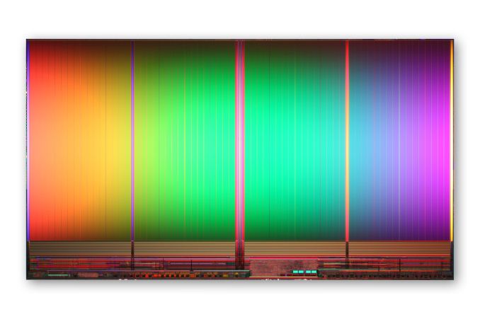
Andrew Walker's  vertical channel 3D NAND based on Chipworks’ cross section of Samsung’s 86 Gbit 32-layer 2nd generation V-NAND


The article below calculate cell size based on Techinsights teardown and wonders about benefits of this technology. However, there are key benefits for Samsung due to the difference in yield and cost of increasing the number of CVD layers vs reducing photolithography layers and masks cost and the associate increase in yield.

More from November 2012 -  3D NAND flash is coming


A 2009 patent application by Samsung for this technology is - US20100155810


Ron
Insightful, timely, and accurate semiconductor consulting.
Semiconductor information and news at - http://www.maltiel-consulting.com/


Samsung’s 3D V-NAND Flash Product: Ceaselessly Marching

What a feast of information Techinsights has given us on Samsung’s 32-layer 3D V-NAND product! By adding dimensions to the cross sections and including the orthogonal direction, we can now add to what we discerned last time and see how Samsung has built this engineering wonder. As a reminder, Figure 1 shows what I thought was a reasonable guess based on Chipworks analysis.
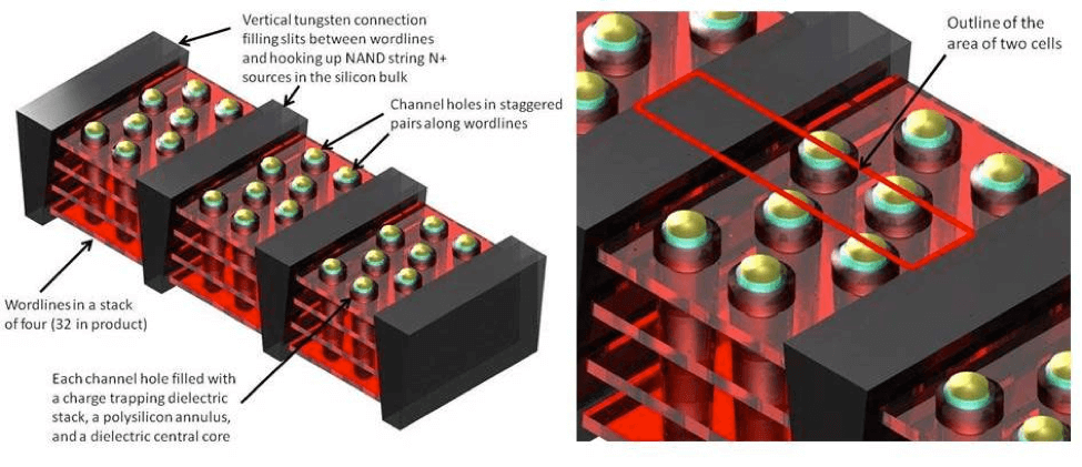
Figure 1: Generic vertical channel 3D NAND based on Chipworks’ cross section of Samsung’s 86 Gbit 32-layer 2nd generation V-NAND.
Notice that I couldn’t add real dimensions at the time. Now we can. But let’s first look at what Techinsights has provided. Figure 2 shows the die with a measurement bar allowing us to come out with the following: die size = 87.4 mm²; array efficiency = 66%.
FIGURE 2 – Die photo of Samsung’s 86 Gbit 32-layer 2nd generation V-NAND (courtesy Techinsights).
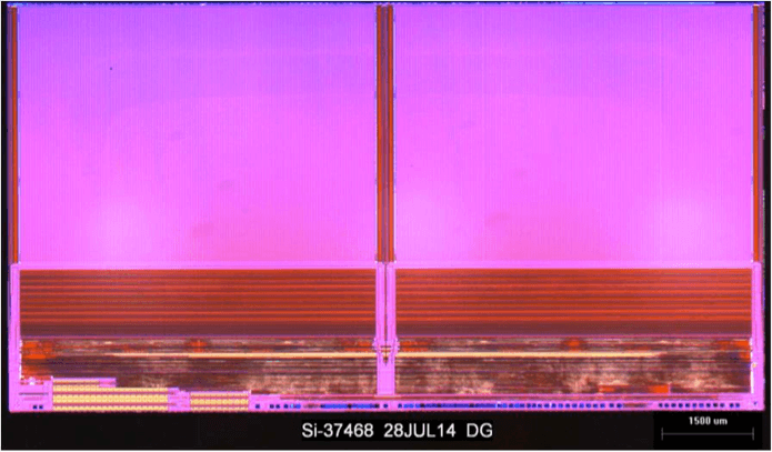
Figure 2: Die photo of Samsung’s 86 Gbit 32-layer 2nd generation V-NAND (courtesy Techinsights).
Figure 3 shows how the wordlines are connected in a staircase fashion. A space of about 20µm is needed.
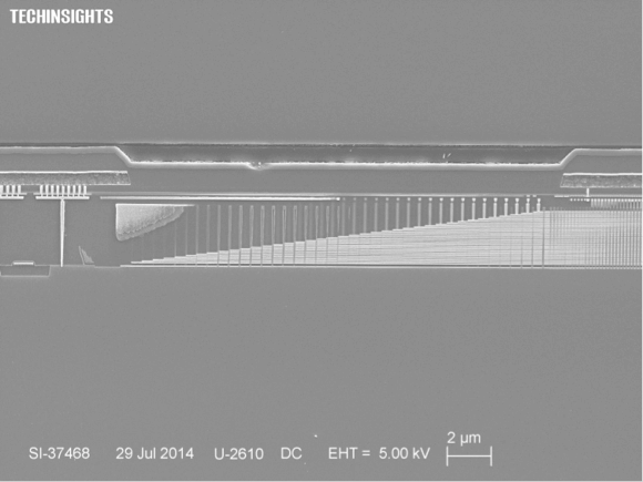
Figure 3: How Samsung connects to the wordlines in the array (courtesy Techinsights).
Figure 4 shows a SEM cross section made at the top of the array stack. This is similar to the one from Chipworks but now with the all-important measurement bar. With this, the long edge of the outline rectangle for two cells given in Figure 1 above is about 725nm. Also, the channel hole pitch in the same direction between the vertical tungsten slits is about 240nm. Don’t worry about remembering these numbers – we’ll summarize at the end in a figure.
Figure 4: Cross section of Samsung’s 86 Gbit 32-layer 2nd generation V-NAND at the top of the stack (courtesy Techinsights).
Figure 5 shows a beautiful cross section TEM image taken at the bottom of the stack and shows how the whole 3D memory array connects up to the wafer substrate.There are some interesting points to be highlighted from this, namely:
  1. The gate all-around access device at the bottom of the stack has a crystalline channel that looks like it has been epitaxially grown from the substrate. If you look carefully, you can make out where the epitaxial growth started which would have been the bottom of the channel hole etched into the wafer substrate.
  2. The polysilicon channel material rests on this pedestal of epitaxial silicon at the bottom of the hole.
  3. The vertical tungsten slits reach through to the silicon substrate which is probably where the NAND N+ doped sources are.
  4. The vertical tungsten slits are laterally isolated from the gate all-around tungsten wordlines.
  5. Vertical tungsten slit-to-slit space (the long edge of the outline rectangle for two cells given in Figure 1) is 730nm.
  6. Hole-to-hole pitch lying between the vertical tungsten slits is 245nm.
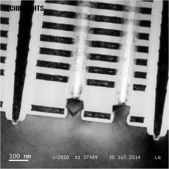
Figure 5; Cross-section TEM of Samsung’s 86 Gbit 32-layer 2nd generation V-NAND at the bottom of the stack (courtesy Techinsights).
Figure 6 shows another beautiful TEM image of the channel holes taken staring down the holes. This one surely wins the prize! It looks like the picture’s y-axis aligns with the direction of the wordlines and the x-axis with the bitlines. In other words, the y-axis is orthogonal to the plane of Figures 4 and 5 above.
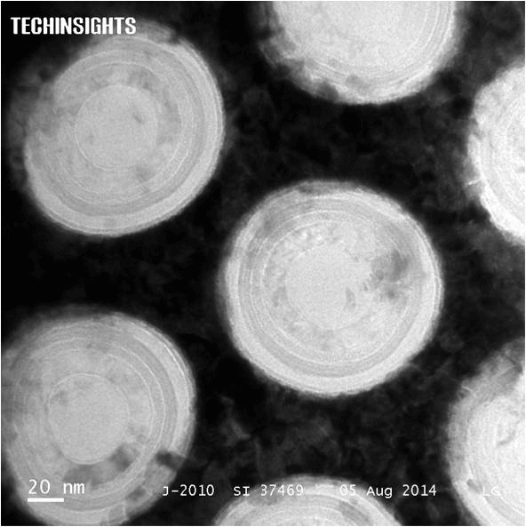
Figure 6: – TEM of Samsung’s 86 Gbit 32-layer 2nd generation V-NAND looking down the channel holes (courtesy Techinsights).
Figure 6 allows us to derive the following information:
  1. Hole-to-hole pitch to make it equivalent to the sectioned holes in the plane of Figures 4 and 5 (bottom left channel hole to bottom right channel hole in Figure 6) = 260 nm.
  2. Hole-to hole-pitch in the orthogonal direction (distance between a horizontal line in Figure 6 through a hole and another horizontal line through the hole that is placed offset to the first hole) = 80 nm.
  3. Diameter of channel hole (before ONO, polysilicon and dielectric core have been deposited) = 120nm.
  4. ONO thickness = 22 nm.
  5. Channel polysilicon thickness = 11 nm.
By taking the critical dimensions from the highest resolution TEM photo (Figure 6) since this will probably be more accurate than the other photos, we can redraw Figure 1 with the dimensions needed to calculate cell size. Note that the vertical tungsten slit to slit dimension has been scaled up slightly from that found in Figure 5 based on the hole to hole dimension calculated in Figure 6.
The final result shown in Figure 7 has two cells in a box of 775nm x 80nm. Therefore, the physical cell size on each layer is around 31000 nm². This is certainly more aggressive than what I had calculated previously but is still around 20F2 where F is 40 nm and remains around 24 times the area of Micron’s 16nm 2D cell.
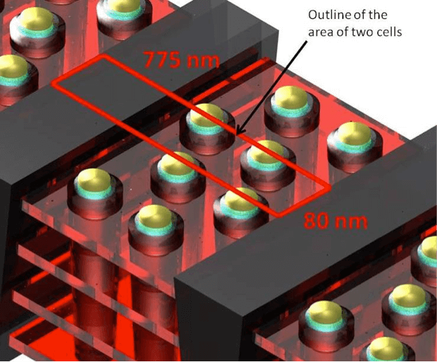
Figure 7: – Final dimensional result for a box containing two physical cells in each layer. The effective physical cell size is 31000 nm².

Thursday, December 11, 2014

Semiconductor Manufacturing 2015 Demand

Key new drivers for new semiconductor fabrication tools is advancing FinFETs 20nm to 16nm/14nm with reasonable yield, and the pace of implementation of 3D NAND. 

Ramp up of 3D flash manufacturing tools will really happen only in 2016 due to length of the development cycle.


In lithography, multi-patterning will continue to be used while EUV continue to faces difficulties. More details are below.


Ron
Insightful, timely, and accurate semiconductor consulting.
Semiconductor information and news at - http://www.maltiel-consulting.com/


Fab Tool Biz Faces Challenges In 2015

After a slight downturn in 2013, the semiconductor equipment industry rebounded and experienced a solid upturn in 2014. The recovery was primarily driven by tool spending in the foundry and DRAM [KC]sectors.
Another big and ongoing story continued to unfold in 2014. In late 2013, Applied Materials announced a definitive agreement to acquire Tokyo Electron Ltd. (TEL) for $9.3 billion. The deal was supposed to close in the second half of 2014. But now, the completion of the deal has been pushed out into 2015 amid a host of complicated regulatory issues.
In fact, the fate of the Applied-TEL deal is just one of the many burning issues for the industry in 2015. The other issues are also clear:
• Will IC-equipment vendors see an upturn or a downturn in 2015?
• What are the drivers?
• Will 450mm fabs, EUV [] and 2.5D [KC]/3D IC [KC] stacked die really happen?
• Will the equipment industry continue to see more acquisition activity in 2015?
The industry continues to consolidate and for good reason. At each node, there are simply fewer customers to serve in a maturing market. “More industry consolidation is needed in several areas, notably in process control and in the components/consumables market, where companies like MKS Instruments, Entegris and others participate,” said Patrick Ho, an analyst at Stifel Nicolaus. “So, will we see (acquisition activity) in 2015? There is a greater likelihood that the smaller players may combine with one another, versus any of the large players taking out the small players. My rationale: the big players are either busy, such as Applied and TEL, or content in their current positions for now. Longer term, we still need one more big deal to occur to further consolidate the space.”
Bold predictions
It’s difficult to predict the future, but there are signs that the Applied-TEL deal will get completed in 2015. So far, the deal has been approved by regulatory bodies in some countries, but not in others. “The deal gets done at some point,” Ho said. “Any deal of this size and scope, particularly when you’re dealing with a relatively consolidated customer base, will likely garner more scrutiny and even some pushbacks from customers. But like many other large deals, I believe ultimately it gets done with perhaps a few contingencies added on to the final deal.”
Another lingering issue is the IC-equipment forecast for 2015. There are mixed signals in the market. Economic growth remains sluggish in many countries. The worldwide geopolitical landscape is troubling. And in the electronics market, the two main catalysts for growth—smartphones and tablets—are showing signs of a slowdown.
As a result, the outlook is cloudy for tool vendors. In fact, citing the slowdown in mobile products and other factors, some are already lowering their forecasts for 2015. In its latest forecast, Gartner projected that semiconductor capital spending and the wafer fab equipment (WFE) market would grow by 11.4% and 17.1%, respectively, in 2014.
For 2015, Gartner currently predicts that semiconductor capital spending and WFE will grow by 8.8% and 11.1%, respectively. “At the moment, those numbers will probably come down a bit, as 2015 does not appear as robust as it did three months ago,” said Dean Freeman, an analyst with Gartner. “WFE for 2015 will be in the 5% to 10% range and CapEx will be closer to 5%. Much of this is dependent upon how much Samsung spends in Q4.”
Many other analysts have a similar forecast for 2015. But on the down side, the ATE market faces a possible downturn in 2015.
Drivers—DRAM, finFETs and NAND
Looking beyond the numbers, tool vendors are in the midst of the most challenging period in the industry’s history. Chipmakers are making a major transition from planar structures to various 3D-like architectures, such as 3D NAND, finFETs [KC] and stacked die.
Toolmakers, in turn, must develop new and advanced systems to meet customer requirements. But the cost to develop new tools is soaring out of control. And yet, there are fewer leading-edge customers at each node.
On the other hand, the shift towards new chip architectures are becoming the “inflection points”—or engines for growth–in the equipment industry, said Doug Bettinger, executive vice president and chief financial officer at Lam Research [], at a recent conference. “(The inflection points include) the move towards multi-patterning. That’s an enormous driver of growth,” Bettinger said. “It’s also the move to finFET from planar. It’s planar to 3D NAND, as well as the move to 3D packaging.”
In 2015, the big driver for fab tool orders will likely reside in the foundry segment, where GlobalFoundries [], Samsung and TSMC [] are making a transition from planar transistors at 20nm to finFETs at 16nm/14nm. Intel Corp. []is already ramping up its second-generation finFETs at 14nm.
For the foundry segment alone, WFE is expected to grow 5% to 10% in 2015, according to Stifel Nicolaus’ Ho. But tool orders for the finFET ramps are also somewhat dependent on one major factor—yield. The foundries, including Intel, are struggling with finFET yields. “With finFET, it will be a question of the magnitude of spending related to yields,” Ho said.
For DRAM, WFE is expected to grow 10% to 15% in 2015. And in NAND, WFE is projected to grow 5% to 10%, according to Stifel Nicolaus. In fact, the DRAM [KC] market remains strong. There could be a shortage of 2D NAND capacity in 2015. But with the exception of Samsung, vendors continue to push out their 3D NAND ramps.
“The timing of 3D NAND has been pushed out due to yields and demand, but the NAND flash industry will eventually transition to this technology,” Ho said. “The cost basis for planar NAND is still more attractive, so I believe the players will try and take advantage of this for two more nodes.”
Others also see a mixed picture in 2015. “In NAND, 3D spending is expected to be broader and larger, but it still lags planar spending until 2016. However, our customers are seeing diminishing gains from planar and (the) 3D adoption is inevitable. DRAM supply is expected to remain tight with strong potential for capacity additions,” said Gigi Lai, senior director of strategic marketing at Applied Materials. “Overall, we expect wafer fab equipment spending will be higher (in 2015), driven by the foundry finFET battle, broader investments in 3D NAND, and increasing DRAM spending.”
450mm and EUV
It’s safe to say that 450mm will not be a factor in 2015. In fact, the industry has put 450mm technology on hold for the foreseeable future. For now, 450mm is too expensive and the benefits are marginal.
But in 2015, the industry will keep a close eye on ASML’s ongoing efforts to put extreme ultraviolet (EUV) lithography into production. “If you look at the (recent) eBeam Initiative [] survey, it indicates that there is a little bit of an increase in the skepticism in EUV,” said Aki Fujimura, chairman and chief executive of D2S. “The survey echoes the statements from many in the industry: ‘We still want (EUV) to happen.’ But publicly, everyone is saying: ‘I don’t know if we can count on it. So we better have backup plans in place.’ “
Barring a major breakthrough in EUV, chipmakers will use 193nm immersion and multiple patterning for both 16nm/14nm and 10nm. “It’s not the question whether you can do (multiple patterning). Technically, it is possible. The question is if it’s economically viable. Certainly, the economic viability answer is very different, depending on who you are,” Fujimura said.
Backend blues
For years, meanwhile, the industry has been talking about the development of 2.5D and 3D chips using through-silicon vias (TSVs). So far, though, 2.5D/3D technology is taking longer than expected amid a number of cost and technical challenges. “We have stuff in production today. But again, these are high-performance applications,” said Jan Vardaman, president of TechSearch International. “Besides Xilinx, there are other people that are developing products using an interposer that should come out in 2015.”
So when will 2.5D/3D stacked die hit the mainstream? “These are new architectures,” Vardaman said. “New architectures take a long time to develop and you have to sort them out carefully.”
The ATE industry, meanwhile, is expected to grow by 20% in 2014. That was driven by booming demand for test in the mobile-based application processor space. Not long ago, Pacific Crest Securities projected that the ATE market would grow by 10% in 2015. But the firm recently lowered its forecast and now projects a 2% decline for ATE in 2015.

Friday, December 5, 2014

Apple Ask Samsung for iPhone 6 Parts

The flash memory bug of TLC performance versus MLC leads Apple to fix the memory IC controller and move from MLC to TLC NAND. It takes about a year to implement such changes. In the meantime, Apple looks to Samsung to provide MLC NAND (see the article below).


This is just another example of the limitations that the consolidation of semiconductor fabrication companies cause on their customers such as Apple. More about semiconductor industry consolidation from March 2012 Moore's Law Slowwwing and from February 2013 Semiconductor Moore's Law Running out of Money.

Ron

Insightful, timely, and accurate semiconductor consulting.Semiconductor information and news at - http://www.maltiel-consulting.com/


Samsung to Provide Parts for Apple’s iPhone 6 and 6 Plus in Order to Fix Huge Bug

Samsung to Provide Parts for Apples iPhone 6 and 6 Plus in Order to Fix Huge Bug Apple iPhone 6 and iPhone 6 Plus 300x225Samsung and Apple have been at war with each other for a long time due to a legal issue where the American tech giant sued Samsung for copying its iPad design. The trial turned out well in the end for Samsung, who continued to heavily criticize Apple and taunt the iPhone 6 and the iPhone 6 Plus devices in their promos and video adverts.
Taking this into consideration, it comes off as a huge and ironic surprise that the South Korean tech company will be providing parts to Apple. Apparently, there have been some discussions between the two tech companies in order to obtain NAND flash memory chips, as Apple needs some supplies of the triple-level cell NAND flash used in the iPhone 6.
Samsung to Provide Parts for Apples iPhone 6 and 6 Plus in Order to Fix Huge Bug Samsung Apple iPhone 6 and iPhone 6 Plus 300x200The higher capacity iPhone 6 handsets are apparently experiencing constant crashes and reboots, and apparently it’s because of the TLC memory. Naturally, Apple has to fix affected devices as soon as possible, especially when you think about how much money people spend on them. Apple’s products have some of the steepest price tags in the tech industry, but the quality has been heavily degrading over the years, making it look like Apple has no quality control. Besides supplying parts for Apple, Samsung will be making batteries for the iPhone 6 as well, according to Business Korea. This has been happening for a while, but Apple has been trying to reduce its reliance on Samsung components for its devices.
It seems that the two companies are going to bury the hatchet, but this could be strictly business-related, so we’ll have to wait and see.

Thursday, December 4, 2014

3D Flash Race:Intel vs Samsung

Following Samsung development of V- NAND Intel introduce their version of 3D NAND (see below). One of the benefits of 3D flash memories is the capability of using larger design rules such as 30-40 nm instead of scaling the design rules to smaller than 20nm.

One of the key problem of shrinking to smaller design rules than 20nm is the cost and complexity of multi-patterning photolithography and EUV lithography difficulties (ASML: Next-gen chipmaking tool ready forproduction in 2016 ). In addition, the reliability of the flash memory degrades when the memory cells become too close to each other.

"Samsung consciously went from a 24-layer 128Gbit MLC die to a 32-layer 86Gbit MLC die. In other words, Samsung could have upped the die capacity to ~170Gbit by just adding the extra layers, but the company chose to go with a smaller die instead. Smaller capacity dies have advantages in performance (higher parallelism) and applicability because eMMC/microSD devices have very strict die size constraints, "

Samsung only use 24 layers in fabricating the chips in order to increase the yield, which reduces the cost of working dies on each wafer. Adding layers that has to be manufactured with precise alignment and low defect density lengthen the learning curve of fabricating working dies. Intel is trying to catch up with Samsung which is already making the second generation of 3D NAND (Samsung 3D Process Pioneers Next Gen Semiconductor Devices ).


Ron
Insightful, timely, and accurate semiconductor consulting.
Semiconductor information and news at - http://www.maltiel-consulting.com/


Intel's 3D NAND to Ship in H2'15: 256Gbit Die

 & 32 Layers

by Kristian Vättö on November 25, 2014 5:20 AM EST
Last Thursday in its annual Investor Meeting Intel revealed the first details of its 3D NAND technology and announced that it will begin the shipments of 3D NAND in the second half of 2015. While Intel's investment in 3D NAND hasn't been a secret, the company has been relatively quiet about any specifics and the vital specs such as the number of layers and die capacity have remained unknown. In Thursday's webcast, Rob Crooke, Senior VP and General Manager of Intel's non-volatile memory group, disclosed that Intel's first generation 3D MLC NAND die will be 256Gbit (32GB) in capacity and will consist of 32 layers. The technology also enables a 384Gbit (48GB) TLC (3-bit-per-cell) die as we have learned over the years.
Intel claims that its 3D NAND is the most cost effective on the market and bases this on the fact that its die is 256Gbit whereas Samsung's is only up to 128Gbit at the moment. I'm not sure if I buy Intel's claim because while it's true that a higher capacity die results in higher array efficiency (i.e. peripheral circuitry takes less area), Samsung consciously went from a 24-layer 128Gbit MLC die to a 32-layer 86Gbit MLC die. In other words, Samsung could have upped the die capacity to ~170Gbit by just adding the extra layers, but the company chose to go with a smaller die instead. Smaller capacity dies have advantages in performance (higher parallelism) and applicability because eMMC/microSD devices have very strict die size constraints, so that might be a part of the reason why Samsung's strategy is so different from Intel's and Micron's. 
NAND Die Size
As the graph above shows, Intel's/Micron's NAND dies have historically been larger than the competitors', so the die capacity alone isn't enough to dictate whether Intel's 3D NAND is more cost efficient than Samsung, especially because both have 32 layers. Unlike Samsung, Intel didn't reveal the lithography that is used to manufacture the 3D NAND, but I would say it's safe to assume that the lithography is in the order of 30nm or 40nm because the whole idea of 3D NAND is to move away from multi-patterning to cut costs and with today's technology the smallest pitch of single-patterning is somewhere between 30nm and 40nm. Either way, it will be very interesting to see how Intel's 3D NAND stacks up against Samsung's because there are also some structural differences that affect the production cost as well as performance and endurance, but I'll save the structural analysis for a future article.
Intel said that 3D NAND technology will enable +10TB SSDs in the 'next couple of years', but it wasn't clear whether that is with first generation 3D NAND or some later generation with more layers and higher die capacity. Currently Intel's lineup tops out at 2TB (P3700 & P3600) with a 128Gbit die, so the 256Gbit die alone isn't enough to bring the capacities above 10TB. With effective controller development it should certainly be possible to build a 10TB SSD with a 256Gbit die, although I'm still inclined to believe that Mr. Crooke was referring to second or third generation 3D NAND with his statement. 
Similar to Intel's previous NAND efforts, 3D NAND has been jointly developed with Micron and will most likely be manufactured in the co-owned Utah plant as Intel sold its share in other fabs a couple of years ago. Interestingly enough, Mr. Crooke said that they also have the ability to bring 3D NAND production to an Intel fab, although to me that sounded more like a statement of technological possibility rather than a hint of future strategy. I wouldn't rule it out, though, but like Mr. Crooke said in the Q&A, Intel needs to have significant competitive advantage for it to make sense. In the past Intel's NAND technologies have generally been slightly ahead of the rest of the industry, but at least as of now Intel doesn't seem to have any substantial advantage in 3D NAND technology as Samsung is already shipping a 32-layer die and will likely ship a 48-layer die before Intel ships its 32-layer product.
All in all, we'll likely get more crumbs of information as the second half of 2015 gets closer. Given Intel's recent SSD strategy, I expect 3D NAND to first find its way to enterprise-class SSDs, but we'll see soon enough.