PORTLAND, OR — Every digital semiconductor manufacturer and foundry in the world is trying to build 3D FinFETS that rival Intel, which is so far leading the pack by several years. Hot on Intel's heels is IBM, which just signed a deal to
turn its fabs over to GlobalFoundries (which has already licensed Samsung's FinFET process that, according to Rick Doherty, research director of The Envisioneering Group, told EE Times stems from early IBM/GlobalFoundaries discussions). TSMC, AMD, Freescale, and others claim to be hot on Intel's and IBM's trail, but have yet to prove it.
With that background, the "dueling technologies" session over FinFET designs being held at the IEEE International Electron Devices Meeting (IEDM, December 15 until December 17, 2014, in San Francisco) looks to be a knock-down, drag-out fight.
"The IEEE's use of the phrase 'dueling technologies' is right!" Doherty told us. "Engineers at IEDM will pass muster on the amazing advances of IBM and Intel first with applause, and later, with purchase orders."
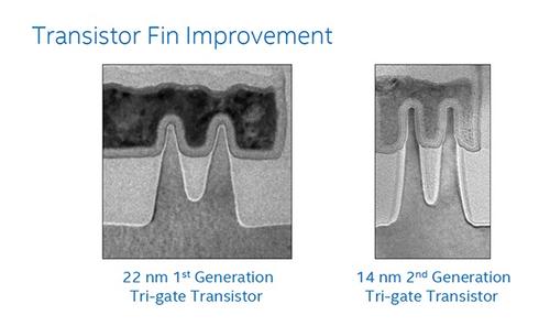
The size of transistor gates and "fins," especially to interconnection, were reduced by more than a third from the previous generation of technology.
(Image: Intel)
Envisioneering believes the IBM FinFET details to be revealed at IEDM lean towards bolstering the Samsung/GlobalFoundaries FinFET technologies already being integrated into Global’s 14 nanometer processes.
"The combinations of dense memory, scalable power budgets and SoCs up to 600 square millimeters strongly point to these IEDM features being available on IBM silicon from Global," Doherty told us. "And possibly available to broader Global customers. What is not yet known is whether these technologies will be build upon the Samsung suite, or might become an alternative FinFET offering from Global."
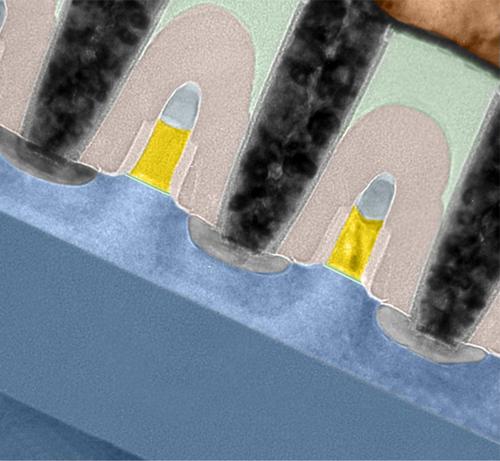
Built on a fully depleted SOI technology base, IBM's 3D, FinFET architecture retains the advantages of SOI over bulk-based planar technologies, which IBM claims is a simpler manufacturing process, with isolation by structure, not doping, low-voltage operation, and lower power.
(Image: IBM)
Either way, Doherty told us that the winners here are customers of both Global and Intel.
"At the IEDM, system and silicon architects will start determining the best applications and markets for each. Intel has given a clear commitment to its novel FinFET designs," Doherty told us. "Global’s choice of two FinFET techniques will likely attract SoC, mobile and high performance users looking for custom solutions."
The biggest difference between IBM's and Intel's approach is that Intel -- as usual -- has taken the traditional bulk silicon approach to developing its FinFET design resulting in a a two- to four-year lead on its competitors in perfecting its approach. Intel has been manufacturing FinFETS in volume since 2011 starting with its 22nm Ivy Bridge and later Haswell micro-architecture processors. More recently it announced successfully transferring of the technology to its 14nm Broadwell micro-architecture which it is the centerpiece for its latest
Core M processor family.
IBM, on the other hand, has take a more experimental approach using more expensive silicon-on-insulator (SOI) substrates that it claims simplify the manufacturing process, allow lower-voltage operation, which means lower-power chips in the long run.
FinFETS were designed to mitigate the leakage effect of short-gate transistors, and have proven to work with or without SOI. By wrapping the gate around the "fin" channel it is possible to fully or nearly-fully deplete the channel when its off leaving very little leakage current to overheat chips.
According to IEDM, Intel will reveal its processing secrets including its doping technique to prevent current leakage under the fins and to maintain very low doped fins, resulting in mitigation of variation, its use of two levels of air-gap-insulated interconnects at 80-and-160nm minimum pitches, yielding a 17% reduction in capacitance delays; eight layers of 52nm pitch interconnects embedded in low-k dielectrics; an embedded 140Mb SRAM memory with a tiny cell size of 0.0588 square micrometers. The fully saturated drive currents are significantly higher than for Intel's 22nm first-generation FinFETs (improvements of 15% for NMOS and 41% and PMOS transistors. Intel will also discuss how it achieved such high-aspect ratio rectangular fins only 8nm wide and 42nm high, according to IEDM. All Intel transistors are operating at a supply voltage of only 0.7 volts.
IBM counter argumentIBM will describe its SOI approach to building 14nm FinFETs, emphasizing that its insulated substrates are worth the extra money the wafers cost because of the processing steps they reduce to isolated devices from one another. Its latest 14nm FinFETs are 35% faster than its planar 22nm transistors and use an operating voltage of 0.8 volts.
IBM will also claim the world's smallest and densest DRAM cells ever demonstrated, taking up just 0.0174 square micrometers. IBM will also describe its unique dual-workfunction process, for both low power and high speed, by virtue of optimizing the threshold voltages of both NMOS and PMOS transistors without mobility degradation in the channel, according to IEDM.
IBM will also brag about its 15 levels of copper interconnect to distribute power and clocks across an entire 600 square millimeter complex SoC for everything from video game consoles to corporate-caliber data centers.
Intel's paper will be called "A 14nm Logic Technology Featuring 2nd-Generation FinFET Transistors, Air-Gapped Interconnects, Self-Aligned Double Patterning and a 0.0588µm2 SRAM Cell Size."
IBM's will be called "High Performance 14nm SOI FinFET CMOS Technology with 0.0174µm2 Embedded DRAM and 15 Levels of Cu Metallization."
— R. Colin Johnson, Advanced Technology Editor,
EE Times


