Showing posts with label SSD. Show all posts

Monday, December 7, 2015

Intel's 3D XPoint Bottlenecks

While Intel's 3D XPoint technology will improve the speed of the CPU communicating with the memory, it will uncover new bottlenecks. The overall system speed is always limited by the weakest link in the chain. 3D XPoint will improve the overall system speed (based on Intel's data). However, depending on specific system setups and the details of their operations, there will be new bottlenecks that will limit the improvement of this new technology.

We saw similar evolution when SSD technology was implemented with new bottlenecks popping up over the last +8 years ( SSD The Next Killer App in NAND Flash - Jim Elliott / Samsung ) .  For example, there are still a lot of issues with storing data in cache of an SSD system as the cache  memory gets filled. See - Why Solid-State Drives Slow Down As You Fill Them Up and How can SD cards be faster than SSDs?


Ron
Insightful, timely, and accurate semiconductor consulting.
Semiconductor information and news at - http://www.maltiel-consulting.com/


Intel’s 3D XPoint fixes bottlenecks


bottleneck-constraint-lean-managementChipzilla and Micron have been working on 3D XPoint technology which they say will close the performance gap between memory, CPU, and networking.
Until now details of the project have been kept under wraps, but now it seems the pair are keen to talk about it. All Intel would say is that it promised about 1,000 times the performance of NAND flash, 1,000 times the endurance of NAND flash, and about 10 times the density of DRAM.
3D XPoint technology is a 3D stacked memory with high-speed interconnects that can be used like DRAM and like flash storage.
Intel CEO Brian Krzanich is now saying that Intel will sell the memory under the Optane brand, and The Next Platform.
Memory is a bottleneck forcing CPUs to wait. Krzanich Optane would speed things up so processors are no longer waiting for data to arrive from memory or storage, in this case flash drives.
Krzanich showed a pair of matching servers. One server had Intel’s P3700 NAND PCI Express SSD and the other was a prototype Optane SSD. The Optane SSD outperformed the P3700 by 4.4 times in IOPS with 6.4 times less latency.
He said that Intel would release Optane next year and will “transform how we think about data and memory and storage.” The company will also come out with Optane DIMMs later this year for early testers. These will combine the performance of DRAM with the capacity and cost of flash.
A two-socket server with Optane DIMMS will have a total of 6 TB of addressable memory, “virtually eliminating paging between memory and storage, taking performance truly to a whole new level.”
- See more at: http://www.techeye.net/chips/intels-3d-xpoint-fixes-bottlenecks#sthash.n79kXMNz.dpuf

Monday, April 6, 2015

3D Semi. Manufacturing Will Benefit LAM, Applied and Other Semiconductor Equipment Vendors

3D semiconductor chip process demand will have a very large impact on semiconductor equipment vendors over the next several years. Initially it is being implemented only on NAND flash

3D chip manufacturing will be implemented by many other types of semiconductor chips such as DRAM memories and other high density ICs.

Historically chip size has been shrinking by using stringent photolithography processes. 3D chip manufacturing enables shrinking chip size while using more relaxed photolithography processes,

3D chip manufacturing relaxes photolithography, but it adds stringent demands on other semiconductor manufacturing processes such as layers deposition and etch. This will increase the demand for equipment vendors such as Applied Materials and LAM as is discussed in the article below.

More about 3D semiconductor from November 2012 is in-  3D NAND flash is coming


More about the processing difficulties is in Applied Materials talks about 3D NAND flash production .

A 2009 patent application by Samsung for this technology is - US20100155810


Ron
Insightful, timely, and accurate semiconductor consulting.
Semiconductor information and news at - http://www.maltiel-consulting.com/


By Tiernan Ray
Credit Suisse’s chip equipment analyst Farhan Ahmad and chip analyst John Pitzer today write that equipment vendors Lam Research (LRCX) and Applied Materials (AMAT) could both see multiplication of their sales as a result of newer three-dimensional NAND flash memory chips, known as “3-D NAND,” that are becoming more prevalent.
Why are the chips important? 3-D NAND chips have 35% more bits per square millimeter, the authors write, at least in the parts produced by Samsung Electronics (005930KS). With increasing “layers,” that can rise to more than double and perhaps triple the bit density.
As a result of density rising faster than costs, “As the density growth is significantly higher from 2D to 3D, than the CapEx increase from 15nm to 3D, we believe that 3D NAND roadmap can potentially provide a 20%/yr cost reductions for next two years.”
While 3-D NAND has been talked about for some time, the key is that the prices of the products are declining rapidly in the marketplace, as evidenced by Samsung’ ssolid-state drives using the chips, the authors write:
We would note the following recent data points (i) Samsung 3D NAND SSD pricing is now at parity with Planar SSDs. Retail pricing indicates that Samsung’s 3D NAND SSDs have declined 20-25% qtd and are now on price parity with leading planar SSDs. Note that 3D NAND SSD are known to have better reliability relative to 2D NAND SSDs, which makes 3D NAND SSD as better choice at same price points. We believe that recent price reductions are a sign that Samsung is trying to accelerate the adoption of 3D NAND and this could prompt other NAND companies to accelerate adoption of 3D NAND. (ii) SanDisk and Micron 3D NAND announcements are indication that 3D NAND progress is not just limited to Samsung, and there is greater evidence that 3D NAND can significantly reduce cost on NAND (our analysis suggests that 48/64 layer 3D NAND could offer >20% cost reduction over planar). Note that once 3D NAND becomes more economical relative to planar, transition to 3D could accelerate as NAND Companies try to compete on costs. (iii) We are seeing more signs of product wins for 3D NAND. Earlier today Korea Times reported that Samsung’s 3D NAND SSD had secured design wins at GOOG and AMZN data centers. Earlier this month Korea times had also reported that Samsung’s 3D NAND had won the Apple’s MacBook business for next year.
For Lam and Applied, they write,
Our analysis suggests that 3D NAND transition could potentially increase NAND WFE to $9-12bn /year for 2016-2018 versus $5-6bn over last 2 years (assuming 40% bit growth per year). We believe that NAND revenues for LRCX could potentially increase by 3x (or $1.5 bn per year) as 3D NAND accelerates. We also expect AMAT to benefit from the 3D NAND transition but estimate that NAND revenues for ASML will decline by > 50% as litho intensive CapEx for planar NAND is replaced by non litho intensive CapEx for 3D NAND.

Friday, February 20, 2015

3D Flash NAND, SSD Challenges

The article below discusses progress in applying 3D processes in fabrication of next generation flash memory. 


Some of the key challenges in developing this technology are:

"challenges on the manufacturing front. In no particular order, alternating stack deposition, metal deposition, high-aspect-ratio etch and metrology are arguably the most difficult process steps for 3D NAND. “Above all, metrology was the most underestimated and under-invested for the industry’s readiness for vertical NAND,” said Naga Chandrasekaran, vice president of process R&D at Micron Technology. “We have these vertical structures and recessed structures within these vertical spaces, but we cannot measure them today....”


My 1990 patent ( Electrical measurements of the profile of semiconductor devices during their manufacturing process ) would help resolving the vertical Metrology difficulties.


More about the processing difficulties is in Applied Materials talks about 3D NAND flash production .


Ron
Insightful, timely, and accurate semiconductor consulting.
Semiconductor information and news at - http://www.maltiel-consulting.com/


3D NAND Market Heats Up

Chips from Samsung, Intel, Micron being sampled, with others on the way.
popularity
After some delays and uncertainty in past years, the 3D NAND market is finally heating up.
In 2013 and 2014, Samsung was the only vendor participating in the 3D NAND market. Most other suppliers were supposed to ship 3D NAND devices in volumes last year, but vendors pushed out their production dates for various business and technical reasons.
Going into 2015, Samsung continues to expand its 3D NAND production. In addition, Micron and its 3D NAND partner, Intel, have recently begun sampling 3D NAND chips, with production slated for the second half of 2015. Another 3D NAND vendor, SK Hynix, plans to move into pilot production later this year.
As previously stated, the SanDisk/Toshiba duo won’t ship 3D NAND until 2016. Meanwhile, Spansion and China’s XMC recently announced a joint agreement to make 3D NAND, with production slated for 2017.
Still, 3D NAND isn’t expected to move into mainstream production until 2017, which is a year or two later than expected. 3D NAND is the eventual successor to today’s 2D NAND, but 3D NAND is more difficult to make than previously thought. 3D NAND resembles a skyscraper, in which horizontal levels are stacked and then connected using tiny vertical channels.
“(3D NAND) will start to ramp in 2016, but it’s a new technology and it will take time to qualify in applications,” said Greg Wong, an analyst with Forward Insights. “It will gain steam in 2017.”
Still, OEMs want to get their hands on 3D NAND sooner than later. So, 3D NAND customers may be asking themselves some simple questions—What are the challenges? And what will it take to get the technology over the hump?
As it turns out, there are a number of challenges on the manufacturing front. In no particular order, alternating stack deposition, metal deposition, high-aspect-ratio etch and metrology are arguably the most difficult process steps for 3D NAND. “Above all, metrology was the most underestimated and under-invested for the industry’s readiness for vertical NAND,” said Naga Chandrasekaran, vice president of process R&D at Micron Technology. “We have these vertical structures and recessed structures within these vertical spaces, but we cannot measure them today.”
Why 3D NAND?
For the foreseeable future, today’s 2D NAND will remain the mainstream technology due to costs. In 2D NAND, the transistor has two gates. The control gate is on the top of the device. The floating gate is in the middle, which is surrounded by a dielectric.
Thanks to 193nm immersion and self-aligned double/quadruple patterning, vendors have extended planar NAND down to the 1xnm node. But at that node, vendors are struggling to scale the floating gate. “In fact, the floating gate is seeing an undesirable reduction in the capacitive coupling to the control gate,” said Jim Handy, an analyst with Objective Analysis.
2D NAND will run out of steam at 10nm, prompting the need for 3D NAND. Unlike planar NAND, 3D NAND makes use of vertical stacks or layers to increase the densities.
Today, the big market for 3D NAND is solid-state drives (SSDs) for niche-oriented enterprise applications. But as 3D NAND becomes more cost competitive, the devices are moving beyond the enterprise. “We (will bolster) our product competitiveness by expanding V-NAND in all segments of SSDs,” said Ji Ho Pak, vice president of memory marketing at Samsung Electronics, in a recent conference call.
Samsung refers to its 3D NAND technology as V-NAND. So far, the company has introduced two V-NAND devices, including 24- and 32-layer chips, based on 30nm to 40nm design rules.
But even at 32 layers, 3D NAND still does not reach cost parity with 2D NAND, keeping 3D NAND at a price premium. In 2015, though, vendors are expected to ship 40- and 48-layer devices, which will bring 3D NAND closer to the price-per-bit curve with 2D NAND.
“It’s a moving target where the true crossover is in terms of the cost-per-bit,” said Bradley Howard, vice president of the Etch Advanced Technology unit at Applied Materials. “The crossover will probably occur closer to 40 to 48 device stacks, as opposed to the 24 and 32 device stacks you are seeing now.”
Howard is also seeing a big shift in the 3D NAND ramp. “We can see the wave building up over the course of this year, based on the interest in tool buys and product ramps,” he said. “And you will see the big ramps going on probably at the end of this year and into 2016.”
At the end of 2014, there were a total of 60,000 to 65,000 wafers starts per month (wspm) in terms of installed capacity for 3D NAND, said Martin Anstice, president and chief executive of Lam Research, in a recent conference call.
Of that figure, Samsung had around 40,000 wspm of installed capacity, according to Pacific Crest Securities. By the end of 2015, the industry is projected to have a total of 130,000 wspm (plus or minus 10,000) of 3D NAND capacity installed, Lam’s Anstice said.
The new litho: alternating stack deposition
Still, there are some big challenges. To make the technology more cost competitive, vendors must scale 3D NAND well beyond 48 layers. In fact, the number of layers is not determined by traditional lithography. Planar NAND requires advanced lithography, while 3D NAND does not. Because the current 3D NAND devices make use of trailing-edge design rules, the challenges shift from lithography to deposition and etch.
The 3D NAND flow starts with a substrate. Then, vendors undergo the first major challenge in the flow—alternating stack deposition. Using chemical vapor deposition (CVD), alternating stack deposition involves a process of depositing and stacking thin films layer by layer on the substrate.
This process is much like making a layer cake. As a chipmaker adds more layers, the device becomes more complex. “Obviously, with these multiple layers, uniformity, repeatability and low defects are becoming critical,” Applied Howard’s said.
There are other issues. “Those alternating layers require a very precise thickness. They require film and surface integrity between each of the layers. And you have to do that in a cost effective way. If I’m putting down 32, 40 and 64 layers, you don’t want it to take forever,” said Dave Hemker, senior vice president and chief technology officer at Lam Research. “There is also a stress concern. As you put down dielectric films, they could have varying degrees of tensile or compressive stress. With a couple of layers, it’s not really something to worry about. But when you start stacking so many of these layers on top of each other, you can run into problems.”
High-aspect ratio etch
Following that step, a hard mask is applied on the surface and holes are patterned on the top. Then, here comes the next hard part. High-aspect ratio trenches are etched from the top of the device to the substrate.
“It’s not just the aspect ratios, but it’s also how deep we have to go,” Applied’s Howard said. “If you take typical planar NAND, you are looking at 12:1 or 15:1 contacts. In 3D NAND, you are looking at 40:1 to 60:1 high-aspect ratios.”
To illustrate the complexity, Samsung’s initial 24-layer device has 2.5 million tiny trenches or channels in the same chip. Each of them must be parallel and uniform. “You need to have perfectly vertical profiles and they need to maintain the CD,” added Lam’s Hemker.
Metal deposition
After the trenches are formed, the device requires contacts. The device is backfilled with a conductor using a metal deposition step.
“There is a challenge in the metal deposition area,” Hemker said. “Typically, in one of the flows, they will wet etch out a nitride layer and backfill it. We’re seeing a lot of customers’ backfilling it with tungsten. And that’s a tricky deposition, because you are doing a non-line of sight deposition. So you basically have these caves and tunnels in there. You have to go back in there after the fact and put in tungsten metal. If you don’t engineer the process right, you may put in this pre-cursor that wants to plate out metallic tungsten. Given its own way, it could plate out right when it gets into the hole. So you have a lot of ways to create voids.”
Metrology
At various steps, the structure goes through a rigorous metrology and inspection flow. The workhorse metrology tool is the scanning electron microscope, which measures the critical dimensions in chips. Another technology, optical scatterometry, analyzes changes in the intensity of light.
One of the many challenges is to find a defect in a multi-layer 3D NAND stack and determine its exact location. “If you look at a planar device, you can look at the top down and get a feel for what’s going on,” Applied’s Howard said. “In these 3D structures, you start getting into 32 or 48 layers. If there’s something going on somewhere in the middle of that stack, your ability to see it is a challenge.”
The big problem is that the current metrology tools are falling short. “The vertical NAND industry is moving very fast, but the characterization requirements of vertical NAND are significant and we don’t have the right techniques in place,” Micron’s Chandrasekaran said.
3D NAND vendors can use the existing metrology tools, at least to some degree. “The tool says there is a defect, but I can’t see it,” Chandrasekaran said. “You have to do a cross section, and you need to find the defect. Then you wait for an electrical signature. That’s too long.”
The metrology tools are making progress, although somewhat more slowly than the industry wants. “It’s taking the traditional methodology and trying to get a better understanding of the data coming off of it,” Applied’s Howard said. “For example, if you are putting an e-beam on a surface, you are getting electron beams on and secondary electrons are coming off. How to interpret that signal gives you the information. There is a lot of work going in how to interpret the signals. As we get more and more data coming out, the ability to build the right algorithms for interpreting the data will mature over time.”
Still, there is room for innovation in the arena. “Everyone knew inspection would be difficult. But it turned out to be very difficult. That’s one of the areas where there is a lot of opportunity for improvement,” he said.

Thursday, September 18, 2014

SanDisk ULLtraDIMM gaining traction

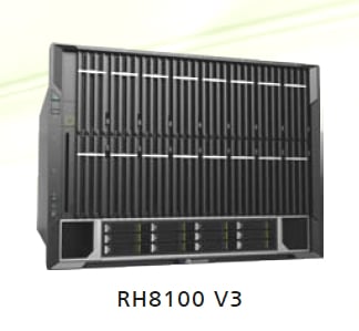
Huawei servers add flash DIMMs to their RH8100 servers (see below).

Are Dell, HP and Cisco next?


More about SanDisk ULLtraDIMMs


Ron
Insightful, timely, and accurate semiconductor consulting.
Semiconductor information and news at - http://www.maltiel-consulting.com/


Huawei: Our servers are a flash in the DRAM – thanks, SanDisk

Chinese box builder flings ULLtraDIMMs into processor memory bus – IBM, Dell next?

Wednesday, July 9, 2014

Will NAND DIMMs take of?

Product like ULLtraDIMM (see article below) can take off  and become a major NAND SSD product line as SanDisk proves it in the market and Diablo Technologies license it to additional SSD suppliers.

More about ULLtraDIMM - Sandisk's future is far from ULLtraDIMM: Diablo tie-up holds promise Goldmine in the making for flash-DIMM server shop


This product is advancing memory system designs similar to the discussion in May 2012 blog - Apple NAND Storage in Upcoming MacBook Pros


Ron
Insightful, timely, and accurate semiconductor consulting.
Semiconductor information and news at - http://www.maltiel-consulting.com/


Will SanDisk Corp's New Product Revolutionize the Storage Industry?

In January, storage provider SanDisk  (NASDAQ: SNDK  ) announced ULLtraDIMM, a new form of flash storage that promises drastic speed increases for high-performance applications. SanDisk already has one big customer, IBM (NYSE: IBM  ) , for its ULLtraDIMMs, giving some early validation to this new technology. Let's take a closer look at ULLtraDIMMs and the effect they might have on the industry.

A bit of background
Storage, such as flash SSDs or hard disk drives, typically sits far away from the CPU and main memory. This means that there is latency due to the time it takes data to travel between the storage device and the CPU. For hard drives, this is not particularly relevant because their own internal latency is much greater than the transport latency. However, for flash, which is completely electronic and therefore much faster than hard disks, this becomes an issue.

The first approach to reducing this latency was to move flash from the drive and onto the PCIe communications bus, a step closer to the CPU. This provided an improvement, but it is not the optimal solution. PCIe still has latency compared to the memory bus, which sits right next to the CPU.

The new technology
Enter SanDisk's ULLtraDIMM, a flash storage that connects directly to the memory bus through the DIMM form factor, just like DRAM memory. Connecting to the memory bus gives ULLtraDIMMs a write latency of under 5 microseconds, compared to around 50 microseconds for PCIe SSDs. The shorter communication distance also means less power consumption, a crucial concern in densely packed enterprise servers.

Sandisk currently provides 200 GB and 400 GB ULLtraDIMMs, and users can add as many ULLtraDIMMs as they have memory slots. ULLtraDIMMs are implemented in a way that makes them look like a normal storage device to the operating system, but achieving this requires modifications to the BIOS which mean that ULLtraDIMMs are not yet plug-and-play devices.

Current and future applications
IBM has already signed up as a customer for Sandisk's ULLtraDIMMs. The enterprise giant has added some functionality to ULLtraDIMMs and rebranded them as eXFlash memory-channel storage. The new technology is available in IBM's X6 family of servers.

According to SanDisk and IBM, memory-channel storage will be useful for applications such as big data analytics, transactional databases, high-frequency trading, and virtualized environments. So far, it seems that IBM's X6 servers have been particularly popular with Wall Street firms. Speaking with EnterpriseTech, SanDisk senior director of marketing Brian Cox said, "we have all kinds of hedge funds begging us to deliver this."

What this means for the industry
It will take several more computer manufacturers to sign on in order to fully validate ULLtraDIMMs as a technology and to reveal the applications where it might best be used. SanDisk's management said that this will require evangelization and a surrounding ecosystem, and that they are continuing to invest in order to bring ULLtraDIMMs to wider adoption.  
Revenue from ULLtraDIMMs is estimated to be small in 2014. However, if ULLtraDIMMs catch on, competitors such as Micron  (NASDAQ: MU  ) (which is increasingly focusing on providing SSDs rather than selling chips as a commodity) will certainly follow with their own versions of memory bus flash. Currently, no other major flash provider is talking about this kind of technology; this means that SanDisk will have first-mover advantage for at least a few quarters.

It's also not clear yet to what extent memory-channel storage might displace PCIe or server-side flash. If the total cost of ownership for an ULLtraDIMM is comparable to or lower than current SSDs, the technology might eventually become the dominant form of flash storage. However, it is also possible that ULLtraDIMMs will complement rather than replace other forms of storage, much like flash itself did with hard disk drives in the enterprise space.

In conclusion
SanDisk has introduced a new form of flash storage called ULLtraDIMM, which sits right next to the CPU on the memory bus and provides much smaller latencies than existing solutions. In a partnership with IBM, ULLtraDIMMs have been shipping to enterprise customers, with expected applications such as high-frequency trading. While the technology certainly sounds promising and might be valuable for both SanDisk and IBM down the line, it's still too early to tell what effect this will have on the storage industry and enterprise computing in general. 
Warren Buffett: This new technology is a "real threat"At the recent Berkshire Hathaway annual meeting, Warren Buffett admitted this emerging technology is threatening his biggest cash-cow. While Buffett shakes in his billionaire-boots, only a few investors are embracing this new market which experts say will be worth over $2 trillion. Find out how you can cash in on this technology before the crowd catches on, by jumping onto one company that could get you the biggest piece of the action. Click here to access a FREE investor alert on the company we're calling the "brains behind" the technology.

Monday, June 16, 2014

SSD Market Share/ SanDisk buys Fusion-io

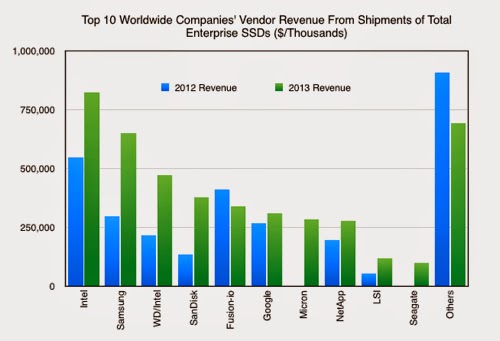
A recent survey by Gartner (see below) shows Intel and Samsung leading in shipment of SSD storage for enterprise.


Ron
Insightful, timely, and accurate semiconductor consulting.
Semiconductor information and news at - http://www.maltiel-consulting.com/


 IBM officially biggest all-flash array shipper - analyst

Gartner AFA data hits the street
By Chris Mellor13 Jun 2014 

No, it isn’t the greatly anticipated all-flash array magic quadrant, but it's great Gartner analysis nonetheless. The number-crunchers at Gartner HWQ have produced a Market Share Analysis: SSDs and Solid-State Arrays, Worldwide, 2013. Yummy. Let’s see what’s inside.
The doc, available as a download from Pure Storage (guess who's done well in the analysis) after registering a few details. It looks at both SSDs and all-flash arrays, which Gartner calls Solid State Arrays (SSAs) and IBM comes out as the leading SSA shipper – with Pure Storage second.
SSAs are defined carefully: ”SSAs are scalable, dedicated, solutions based solely on solid-state semiconductor technology for data storage that cannot be configured with HDD technology at any time. As distinct from SSD-only racks within ECB storage arrays, an SSA must be a stand-alone product denoted with a specific name and model number, which typically (but not always) includes an operating system and data management software optimised for solid-state technology.”
To cut a long story short, Dell and HDS all-flash array products are excluded, as are all-flash versions of – for example – EMC VMAX and VNX, and NetApp FAS arrays.
The SSD category embraces PCIe flash cards and also includes “self-contained solid-state NAND dual in-line memory modules (DIMMs), which must be used in dedicated slots in servers. Mainstream PC SSDs being used in servers are counted in this category due to end consumption.”
We’ll graph the information here, and you can read the detailed numbers by downloading the doc. The SSD info starts with worldwide vendor revenues:
Click chart for larger version
Total SSD revenues in 2012 were $7.2 billion, and in 2013 had risen to $10.99 billion, a 53.1 per cent increase.
Samsung as top dog got most of that with Intel, growing less, at number 2. Look at Sandisk’s rocketing growth up into the no 3 slot, closely followed by Micron. Toshiba held its fifth place but didn’t grow much. WD grew, Fusion-io declined and now we’re in the tail-enders.
Now let’s look at the enterprise SSD market:


Intel is top dog, not second-placed Samsung. WD, with its HGST/Intel SSDs is in third place followed by SanDisk successfully exhibiting its enterprise supplier credentials. Then there’s Fusion-io, which declined 2012 - 2013, Google with its internal use - amazing - Micron is a, we think, in a disappointing sixth place, NetApp a, for it, strong seventh then LSI and Seagate. EMC does not appear at all.
Now for the SSA numbers.
Here are the vendor revenue market share numbers:

Click chart to make it larger.
And here the actual SSA revenues by vendor:

Click chart to make it larger
IBM has had a wildly successful 2013 year, solidly overtaking Violin Memory to claim a dominating number 1 slot. Pure Storage has rocketed to the number 2 position in 2013 while Violin Memory slumped from first place in 2013 to third in 2013, illustrating the new management team’s uphill task. EMC has sprung into fourth place from a standing start and NetApp is not far behind in the fifth slot. Then there’s Nimbus Data and tail-ender Cisco - a dismal showing for the networking behemoth in our view, with startup SolidFire very close behind.
The SSA market was sized by Gartner at $236.5m in 2012, and 182.1 per cent higher at $667.3m in 2013. IBM’s SSA revenues grew at 278.1 per cent, Pure's at a magnificent 642.3 per cent and no other vendor outpaced the market, meaning they lost share.
Now this is artificial, as EMC, Kaminario, SolidFire and HP had no presence in Gartner’s numbers in 2013, but we can assert that Violin Memory, NetApp, Nimbus and Cisco all lost share from 2012 to 2013. With EMC, Kaminario, SolidFire and HP now in the SAA market we might expect these losses to continue in 2014.
The Gartner analysis contains more data, segment metrics and so forth. It’s worth a download and read if you’re interested.
Main takeaway? Big Blue really is big in SSAs, Pure Storage is living up to its hype, and the SSA market is growing at a fast lick. NAND the story goes on


Monday, March 17, 2014

Self Encrypting SSD (SED) to Rescue Security/ Privacy?

The article below discusses benefits of integrating encrypting in the hardware.

"Samsung claims that self-encrypting drives are the solutions to better security...can protect sensitive data better than software solutions because self-encrypting SSDs automatically encrypt information as it's saved to the drive.

A key benefit of SED (Self Encrypting Drive) is the automated process, which makes it difficult for human error leaving the data vulnerable (see Missed Alarms, 40 Mil. Stolen Credit Card Numbers: Target Blew It). In addition, the additional security level of the hardware on silicon chip increase the difficulty for anybody trying to access the data.

Remaining issues in protecting the data:
Is there any way to replicate the encryption key stored on the silicon chip?

Can a government or a malicious vendor duplicate the encryption and transmit it through a back door?

Ron
Insightful, timely, and accurate semiconductor consulting.
Semiconductor information and news at - http://www.maltiel-consulting.com/


Will Self-Encrypting Drives Help Stop Data Breaches?

  • Mar 14, 2014 8:00 AM EST
In light of all the security breaches last year, companies are looking for ways to protect their own and their clients' data. Samsung claims that self-encrypting drives are the solutions to better security software protection. In a recent infographic, the company outlines a few reasons why self-encrypting drives are better for businesses.
In 2012, well over 250 million records with personal information were compromised in security breaches. That same year, the average cost of a data breach was more than five million dollars. Samsung claims this devastating problem can be alleviated with an easy solution: swapping out a PC's hard disk drive for a solid state drive (SSD) with self-encrypting drive (SED) technology. These drives can protect sensitive data better than software solutions because self-encrypting SSDs automatically encrypt information as it's saved to the drive. 
The Perks of SSD with SEDFirst off, data encryption and key management happen in drive hardware so putting in an SSD with SED leads to better security and system performance. Software encryption is just another process on a host device, which makes it more vulnerable to attacks and hinders PC performance when it encrypts data.
Oftentimes employees will turn off software-based encryption, which leads to noncompliance risk. SEDs, on the other hand, cannot be disabled, and encryption transparent to users. There's no need to download special security software to use SEDs either; they meet requirements for enterprise applications and can be controlled by security management software.
Why Self-Encrypting SSD Is the SolutionUsing Crypto Erase technology to wipe out data on your SED is a quick and painless process: the drive simply deletes the active encryption key. Trying to render data unreadable on a hard drive with software-based encryption, on the other hand, can take up a lot more of your time and money.
An additional perk is that SEDs fulfill government and industry requirements that laws like FACTA and HIPAA implement to regulate the security of private electronic data. Several laws also include a Safe Harbor convention for encrypted data, which spares organizations the embarrassment and expense of a public notification of data breaches.
Self-encrypting SSDs costs less than 80 cents per gigabyte, potentially saving millions of dollars for many companies. These drives could be a great tool for companies to use to protect consumer information and avoid the headaches of data breaches. 

Monday, March 3, 2014

Flash NAND, NOR, eMMC Market Growth

NAND market continues to grow while NOR continue to shrink (see article below). 

The reason for NAND dominance were explained on my May 2007 article on Long Term Trends in the NOR and NAND Markets .


Highlights from review of the IHS report in the article below:
"NAND product known as embedded multimedia card (eMMC) enjoyed record shipments in 2013 of more than 1 billion units, up a hefty 49 percent from 687 million in 2012. NAND revenue rose 28 percent to US$25.8 billion.
In comparison, NOR shipments last year fell 10 percent to 606 million units, with revenue down 15 percent to approximately US$3.0 billion....
The evolution of eMMC, in particular, has been rapid, with nearly annual enhancements to performance. As an economical choice for greater flash-memory densities, eMMC has become viable in high-end markets like smartphones and tablets, in which high-density storage capacity is required along with low-power consumption and a small footprint.
Embedded NAND’s utility has also now carried over from smartphones in its early use, to tablets. Last year, eMMC was the standard memory configuration for a vast majority of tablets, the only exception being the Surface Pro from Microsoft, which employs a SATA-interface solid-state drive.
The billion-unit shipment level of eMMC last year is a milestone, Yang remarked, and the product shows the way forward for managed NAND solutions by its deft handling of error correction and enhanced reliability at the solution level."
Ron
Insightful, timely, and accurate semiconductor consulting.
Semiconductor information and news at - http://www.maltiel-consulting.com/


NAND eMMC hits a record year, while NOR Flash shrinks further

 
NAND eMMC hits a record year, while NOR Flash shrinks further
Source: IHS Technology, February 2014

The global memory market presented a vivid picture of contrast last year given the wildly divergent fortunes of its two main segments, with spritely NAND offset by the sobering continued downturn of beleaguered NOR flash, according to a new report from IHS Technology.
On the one hand, the NAND product known as embedded multimedia card (eMMC) enjoyed record shipments in 2013 of more than 1 billion units, up a hefty 49 percent from 687 million in 2012. NAND revenue rose 28 percent to US$25.8 billion.
In comparison, NOR shipments last year fell 10 percent to 606 million units, with revenue down 15 percent to approximately US$3.0 billion.
The overall flash market in 2013 was worth US$28.8 billion, up from US$23.7 billion a year earlier, as shown in the attached figure.
“The key driver to NAND lies in its proliferating use for mobile consumer electronics, exemplified by the memory’s increasingly widespread application in devices like smartphones, tablets and notebook PCs,” said Michael Yang, senior principal analyst for memory & storage at IHS.
“Meanwhile, NOR’s once-broad portfolio of applications in low-end mobile handsets and desktop PCs has mostly matured, and its next killer market has yet to manifest.”
These findings are contained in the report, “Mobile & Embedded Memory Tracker – Q4 2013,” from the Semiconductors & Components service of IHS.
NAND memory, in the form of either raw NAND or eMMC, is now the standard memory used for most smartphones. The only exception is Apple’s iPhone, which uses its own managed NAND memory product.
The evolution of eMMC, in particular, has been rapid, with nearly annual enhancements to performance. As an economical choice for greater flash-memory densities, eMMC has become viable in high-end markets like smartphones and tablets, in which high-density storage capacity is required along with low-power consumption and a small footprint.
Embedded NAND’s utility has also now carried over from smartphones in its early use, to tablets. Last year, eMMC was the standard memory configuration for a vast majority of tablets, the only exception being the Surface Pro from Microsoft, which employs a SATA-interface solid-state drive.
The billion-unit shipment level of eMMC last year is a milestone, Yang remarked, and the product shows the way forward for managed NAND solutions by its deft handling of error correction and enhanced reliability at the solution level.
The rise of eMMC has also bred a new cast of suppliers. While Samsung remains dominant, players like SK Hynix, SanDisk and Toshiba are fiercely competitive and poised to gain ground.
The eMMC space, however, could see challenges this year. With growth slowing in the smartphone and tablet markets, there could be a possible oversupply of the memory type, in the process also leading to a possible large drop in eMMC average selling prices.
The steady decline of the NOR flash market began in 2007 and hasn’t stopped since. At its peak, the NOR market exceeded US$9 billion a year and last hit US$8 billion back in 2006—a far cry from its current numbers.
The NOR picture is also complicated by the contrasting outlook for its two sub-segments.
Parallel NOR, long used in computers for boot-code execution or serving as a storage medium for entry-level cellphones, will see its run in wireless devices come to an end sometime next year.
Parallel NOR will continue to be used in high-level industrial, medical, networking and military applications, but its exit from wireless will be a blow.
Meanwhile, serial peripheral interface (SPI) NOR, rival to parallel NOR, will go on to wider use in both wireless and consumer devices.
SPI NOR’s relative simplicity in design and low manufacturing cost will prove appealing, and the memory will be especially attractive to manufacturers of low-cost cellphones that need to keep a lid on expenses.
The shift from parallel to SPI NOR has also impacted their respective suppliers. Micron Technology and Spansion, the foremost producers of parallel NOR, now also have SPI offerings.
However, both companies have been at pains to differentiate their SPI product from the rest of the pack, in order to stave off the aggressive penetration of other SPI NOR suppliers such as Macronix, Winbond Electronics and GigaDevice.
The ongoing growth of SPI NOR will help offset a shrinking parallel NOR market, but the industry would be healthier if consolidation took place and reduced the number of players to four, IHS believes.
There are five suppliers at present that command 75 percent of the market, along with a spattering of smaller producers that make up the rest of the market.
Even so, there are no quick fixes, with the largest NOR applications disappearing or on their way out, and new deployments like automotive NOR still facing an uphill climb.