Andrew Walker at 3dincites.com analyzes Samsung 3D
V-NAND below.
 |
| Andrew Walker's vertical channel 3D NAND based on Chipworks’ cross section of Samsung’s 86 Gbit 32-layer 2nd generation V-NAND |
The article below calculate cell size based on
Techinsights teardown and wonders about benefits of this technology. However, there are key benefits for Samsung due to
the difference in yield and cost of increasing the number of CVD layers vs
reducing photolithography layers and masks cost and the associate increase in yield.
More from November 2012 - 3D NAND flash is coming
A 2009 patent application by Samsung for this technology is -
US20100155810
Ron
Insightful, timely, and accurate semiconductor consulting.
Semiconductor information and news at - http://www.maltiel-consulting.com/
Samsung’s 3D V-NAND Flash Product: Ceaselessly Marching
What a feast of information Techinsights has given us on Samsung’s 32-layer 3D V-NAND product! By adding dimensions to the cross sections and including the orthogonal direction, we can now add to what we discerned last time and see how Samsung has built this engineering wonder. As a reminder, Figure 1 shows what I thought was a reasonable guess based on Chipworks analysis.
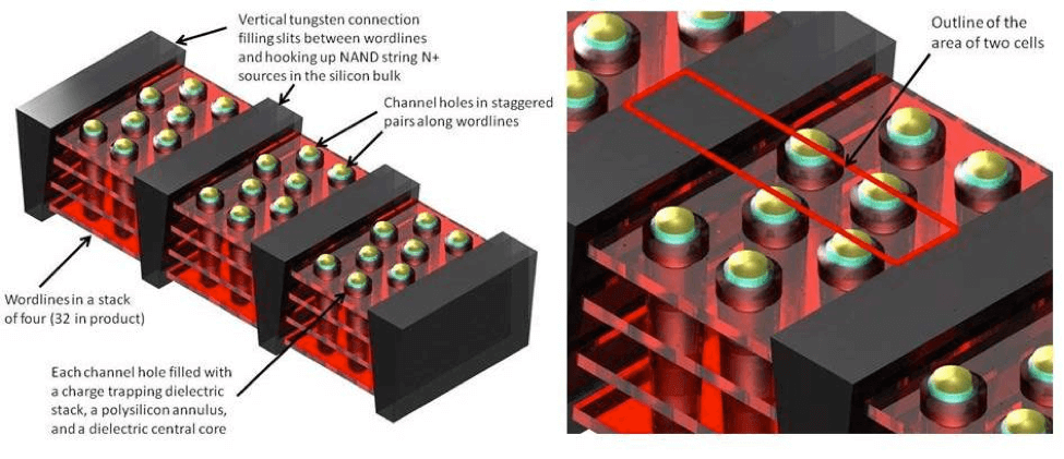
Figure 1: Generic vertical channel 3D NAND based on Chipworks’ cross section of Samsung’s 86 Gbit 32-layer 2nd generation V-NAND.
Notice that I couldn’t add real dimensions at the time. Now we can. But let’s first look at what Techinsights has provided. Figure 2 shows the die with a measurement bar allowing us to come out with the following: die size = 87.4 mm²; array efficiency = 66%.
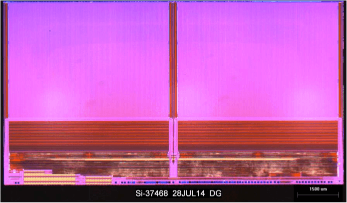
Figure 2: Die photo of Samsung’s 86 Gbit 32-layer 2nd generation V-NAND (courtesy Techinsights).
Figure 3 shows how the wordlines are connected in a staircase fashion. A space of about 20µm is needed.
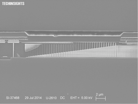
Figure 4 shows a SEM cross section made at the top of the array stack. This is similar to the one from Chipworks but now with the all-important measurement bar. With this, the long edge of the outline rectangle for two cells given in Figure 1 above is about 725nm. Also, the channel hole pitch in the same direction between the vertical tungsten slits is about 240nm. Don’t worry about remembering these numbers – we’ll summarize at the end in a figure.

Figure 4: Cross section of Samsung’s 86 Gbit 32-layer 2nd generation V-NAND at the top of the stack (courtesy Techinsights).
Figure 5 shows a beautiful cross section TEM image taken at the bottom of the stack and shows how the whole 3D memory array connects up to the wafer substrate.There are some interesting points to be highlighted from this, namely:
- The gate all-around access device at the bottom of the stack has a crystalline channel that looks like it has been epitaxially grown from the substrate. If you look carefully, you can make out where the epitaxial growth started which would have been the bottom of the channel hole etched into the wafer substrate.
- The polysilicon channel material rests on this pedestal of epitaxial silicon at the bottom of the hole.
- The vertical tungsten slits reach through to the silicon substrate which is probably where the NAND N+ doped sources are.
- The vertical tungsten slits are laterally isolated from the gate all-around tungsten wordlines.
- Vertical tungsten slit-to-slit space (the long edge of the outline rectangle for two cells given in Figure 1) is 730nm.
- Hole-to-hole pitch lying between the vertical tungsten slits is 245nm.
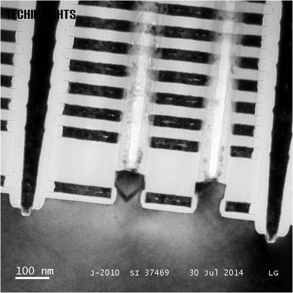
Figure 5; Cross-section TEM of Samsung’s 86 Gbit 32-layer 2nd generation V-NAND at the bottom of the stack (courtesy Techinsights).
Figure 6 shows another beautiful TEM image of the channel holes taken staring down the holes. This one surely wins the prize! It looks like the picture’s y-axis aligns with the direction of the wordlines and the x-axis with the bitlines. In other words, the y-axis is orthogonal to the plane of Figures 4 and 5 above.
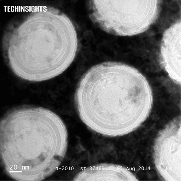
Figure 6: – TEM of Samsung’s 86 Gbit 32-layer 2nd generation V-NAND looking down the channel holes (courtesy Techinsights).
Figure 6 allows us to derive the following information:
- Hole-to-hole pitch to make it equivalent to the sectioned holes in the plane of Figures 4 and 5 (bottom left channel hole to bottom right channel hole in Figure 6) = 260 nm.
- Hole-to hole-pitch in the orthogonal direction (distance between a horizontal line in Figure 6 through a hole and another horizontal line through the hole that is placed offset to the first hole) = 80 nm.
- Diameter of channel hole (before ONO, polysilicon and dielectric core have been deposited) = 120nm.
- ONO thickness = 22 nm.
- Channel polysilicon thickness = 11 nm.
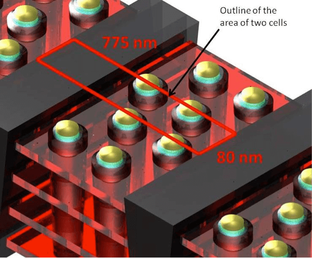
By taking the critical dimensions from the highest resolution TEM photo (Figure 6) since this will probably be more accurate than the other photos, we can redraw Figure 1 with the dimensions needed to calculate cell size. Note that the vertical tungsten slit to slit dimension has been scaled up slightly from that found in Figure 5 based on the hole to hole dimension calculated in Figure 6.
The final result shown in Figure 7 has two cells in a box of 775nm x 80nm. Therefore, the physical cell size on each layer is around 31000 nm². This is certainly more aggressive than what I had calculated previously but is still around 20F2 where F is 40 nm and remains around 24 times the area of Micron’s 16nm 2D cell.
No comments:
Post a Comment